EP0298933A2 - Verfahren zur Herstellung supraleitender Kupferoxid-Schichten - Google Patents
Verfahren zur Herstellung supraleitender Kupferoxid-Schichten Download PDFInfo
- Publication number
- EP0298933A2 EP0298933A2 EP88830295A EP88830295A EP0298933A2 EP 0298933 A2 EP0298933 A2 EP 0298933A2 EP 88830295 A EP88830295 A EP 88830295A EP 88830295 A EP88830295 A EP 88830295A EP 0298933 A2 EP0298933 A2 EP 0298933A2
- Authority
- EP
- European Patent Office
- Prior art keywords
- manufacture
- alloy
- film
- binary alloy
- copper oxide
- Prior art date
- Legal status (The legal status is an assumption and is not a legal conclusion. Google has not performed a legal analysis and makes no representation as to the accuracy of the status listed.)
- Granted
Links
- 238000000034 method Methods 0.000 title claims description 17
- 238000004519 manufacturing process Methods 0.000 title claims description 7
- QPLDLSVMHZLSFG-UHFFFAOYSA-N Copper oxide Chemical compound [Cu]=O QPLDLSVMHZLSFG-UHFFFAOYSA-N 0.000 title 1
- 239000005751 Copper oxide Substances 0.000 title 1
- 229910000431 copper oxide Inorganic materials 0.000 title 1
- 229910002056 binary alloy Inorganic materials 0.000 claims abstract description 15
- 238000001704 evaporation Methods 0.000 claims abstract description 13
- 239000012298 atmosphere Substances 0.000 claims abstract description 5
- 239000000463 material Substances 0.000 claims abstract description 5
- 229910052802 copper Inorganic materials 0.000 claims description 12
- 239000000758 substrate Substances 0.000 claims description 6
- 229910045601 alloy Inorganic materials 0.000 claims description 4
- 239000000956 alloy Substances 0.000 claims description 4
- 230000001590 oxidative effect Effects 0.000 claims description 2
- 229910000765 intermetallic Inorganic materials 0.000 claims 4
- 230000008020 evaporation Effects 0.000 abstract description 9
- 238000010894 electron beam technology Methods 0.000 abstract description 4
- QVGXLLKOCUKJST-UHFFFAOYSA-N atomic oxygen Chemical compound [O] QVGXLLKOCUKJST-UHFFFAOYSA-N 0.000 abstract description 3
- 239000001301 oxygen Substances 0.000 abstract description 3
- 229910052760 oxygen Inorganic materials 0.000 abstract description 3
- 229910002530 Cu-Y Inorganic materials 0.000 abstract 1
- 239000010408 film Substances 0.000 description 13
- 239000000203 mixture Substances 0.000 description 7
- 238000000151 deposition Methods 0.000 description 6
- 238000004544 sputter deposition Methods 0.000 description 4
- 230000008021 deposition Effects 0.000 description 3
- XKRFYHLGVUSROY-UHFFFAOYSA-N Argon Chemical compound [Ar] XKRFYHLGVUSROY-UHFFFAOYSA-N 0.000 description 2
- IJGRMHOSHXDMSA-UHFFFAOYSA-N Atomic nitrogen Chemical compound N#N IJGRMHOSHXDMSA-UHFFFAOYSA-N 0.000 description 2
- 229910009203 Y-Ba-Cu-O Inorganic materials 0.000 description 2
- MCMNRKCIXSYSNV-UHFFFAOYSA-N Zirconium dioxide Chemical compound O=[Zr]=O MCMNRKCIXSYSNV-UHFFFAOYSA-N 0.000 description 2
- 239000007788 liquid Substances 0.000 description 2
- 239000010409 thin film Substances 0.000 description 2
- 229910052786 argon Inorganic materials 0.000 description 1
- 239000012300 argon atmosphere Substances 0.000 description 1
- 238000009835 boiling Methods 0.000 description 1
- 229910010293 ceramic material Inorganic materials 0.000 description 1
- 150000001875 compounds Chemical class 0.000 description 1
- 239000004020 conductor Substances 0.000 description 1
- 230000006866 deterioration Effects 0.000 description 1
- 238000005566 electron beam evaporation Methods 0.000 description 1
- 239000001307 helium Substances 0.000 description 1
- 229910052734 helium Inorganic materials 0.000 description 1
- SWQJXJOGLNCZEY-UHFFFAOYSA-N helium atom Chemical compound [He] SWQJXJOGLNCZEY-UHFFFAOYSA-N 0.000 description 1
- 238000001755 magnetron sputter deposition Methods 0.000 description 1
- 229910052751 metal Inorganic materials 0.000 description 1
- 229910052757 nitrogen Inorganic materials 0.000 description 1
- 238000007750 plasma spraying Methods 0.000 description 1
- 239000004065 semiconductor Substances 0.000 description 1
Images
Classifications
-
- C—CHEMISTRY; METALLURGY
- C23—COATING METALLIC MATERIAL; COATING MATERIAL WITH METALLIC MATERIAL; CHEMICAL SURFACE TREATMENT; DIFFUSION TREATMENT OF METALLIC MATERIAL; COATING BY VACUUM EVAPORATION, BY SPUTTERING, BY ION IMPLANTATION OR BY CHEMICAL VAPOUR DEPOSITION, IN GENERAL; INHIBITING CORROSION OF METALLIC MATERIAL OR INCRUSTATION IN GENERAL
- C23C—COATING METALLIC MATERIAL; COATING MATERIAL WITH METALLIC MATERIAL; SURFACE TREATMENT OF METALLIC MATERIAL BY DIFFUSION INTO THE SURFACE, BY CHEMICAL CONVERSION OR SUBSTITUTION; COATING BY VACUUM EVAPORATION, BY SPUTTERING, BY ION IMPLANTATION OR BY CHEMICAL VAPOUR DEPOSITION, IN GENERAL
- C23C14/00—Coating by vacuum evaporation, by sputtering or by ion implantation of the coating forming material
- C23C14/06—Coating by vacuum evaporation, by sputtering or by ion implantation of the coating forming material characterised by the coating material
- C23C14/08—Oxides
- C23C14/087—Oxides of copper or solid solutions thereof
-
- C—CHEMISTRY; METALLURGY
- C04—CEMENTS; CONCRETE; ARTIFICIAL STONE; CERAMICS; REFRACTORIES
- C04B—LIME, MAGNESIA; SLAG; CEMENTS; COMPOSITIONS THEREOF, e.g. MORTARS, CONCRETE OR LIKE BUILDING MATERIALS; ARTIFICIAL STONE; CERAMICS; REFRACTORIES; TREATMENT OF NATURAL STONE
- C04B35/00—Shaped ceramic products characterised by their composition; Ceramics compositions; Processing powders of inorganic compounds preparatory to the manufacturing of ceramic products
- C04B35/01—Shaped ceramic products characterised by their composition; Ceramics compositions; Processing powders of inorganic compounds preparatory to the manufacturing of ceramic products based on oxide ceramics
- C04B35/45—Shaped ceramic products characterised by their composition; Ceramics compositions; Processing powders of inorganic compounds preparatory to the manufacturing of ceramic products based on oxide ceramics based on copper oxide or solid solutions thereof with other oxides
- C04B35/4504—Shaped ceramic products characterised by their composition; Ceramics compositions; Processing powders of inorganic compounds preparatory to the manufacturing of ceramic products based on oxide ceramics based on copper oxide or solid solutions thereof with other oxides containing rare earth oxides
-
- C—CHEMISTRY; METALLURGY
- C23—COATING METALLIC MATERIAL; COATING MATERIAL WITH METALLIC MATERIAL; CHEMICAL SURFACE TREATMENT; DIFFUSION TREATMENT OF METALLIC MATERIAL; COATING BY VACUUM EVAPORATION, BY SPUTTERING, BY ION IMPLANTATION OR BY CHEMICAL VAPOUR DEPOSITION, IN GENERAL; INHIBITING CORROSION OF METALLIC MATERIAL OR INCRUSTATION IN GENERAL
- C23C—COATING METALLIC MATERIAL; COATING MATERIAL WITH METALLIC MATERIAL; SURFACE TREATMENT OF METALLIC MATERIAL BY DIFFUSION INTO THE SURFACE, BY CHEMICAL CONVERSION OR SUBSTITUTION; COATING BY VACUUM EVAPORATION, BY SPUTTERING, BY ION IMPLANTATION OR BY CHEMICAL VAPOUR DEPOSITION, IN GENERAL
- C23C14/00—Coating by vacuum evaporation, by sputtering or by ion implantation of the coating forming material
- C23C14/0021—Reactive sputtering or evaporation
-
- C—CHEMISTRY; METALLURGY
- C23—COATING METALLIC MATERIAL; COATING MATERIAL WITH METALLIC MATERIAL; CHEMICAL SURFACE TREATMENT; DIFFUSION TREATMENT OF METALLIC MATERIAL; COATING BY VACUUM EVAPORATION, BY SPUTTERING, BY ION IMPLANTATION OR BY CHEMICAL VAPOUR DEPOSITION, IN GENERAL; INHIBITING CORROSION OF METALLIC MATERIAL OR INCRUSTATION IN GENERAL
- C23C—COATING METALLIC MATERIAL; COATING MATERIAL WITH METALLIC MATERIAL; SURFACE TREATMENT OF METALLIC MATERIAL BY DIFFUSION INTO THE SURFACE, BY CHEMICAL CONVERSION OR SUBSTITUTION; COATING BY VACUUM EVAPORATION, BY SPUTTERING, BY ION IMPLANTATION OR BY CHEMICAL VAPOUR DEPOSITION, IN GENERAL
- C23C14/00—Coating by vacuum evaporation, by sputtering or by ion implantation of the coating forming material
- C23C14/06—Coating by vacuum evaporation, by sputtering or by ion implantation of the coating forming material characterised by the coating material
- C23C14/14—Metallic material, boron or silicon
-
- H—ELECTRICITY
- H10—SEMICONDUCTOR DEVICES; ELECTRIC SOLID-STATE DEVICES NOT OTHERWISE PROVIDED FOR
- H10N—ELECTRIC SOLID-STATE DEVICES NOT OTHERWISE PROVIDED FOR
- H10N60/00—Superconducting devices
- H10N60/01—Manufacture or treatment
- H10N60/0268—Manufacture or treatment of devices comprising copper oxide
- H10N60/0296—Processes for depositing or forming copper oxide superconductor layers
- H10N60/0548—Processes for depositing or forming copper oxide superconductor layers by deposition and subsequent treatment, e.g. oxidation of pre-deposited material
Definitions
- the present invention relates to a method for the manufacture of superconducting films having a critical temperature, T c greater than 77 K by the utilization of two binary alloy evaporation sources.
- critical temperature is meant the temperature at which the film becomes super-conducting.
- Such materials having a high superconducting temperature are very economical as they do not have to be cooled to lower temperatures by means of costly liquid helium.
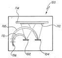
- the drawing shows a representation of an evaporation chamber useful in depositing films of the present invention.
- a method for the manufacture of a deposited film of a superconducting element comprising the steps of:
- the drawing shows an evaporation chamber 100 containing a first binary alloy source 102 which can conveniently be an intermetallic binary alloy of Cu and Y such as Cu1Y1, Cu2Y, Cu4Y, Cu6Y or Cu7Y.
- a first binary alloy source 102 which can conveniently be an intermetallic binary alloy of Cu and Y such as Cu1Y1, Cu2Y, Cu4Y, Cu6Y or Cu7Y.
- a second binary alloy source 104 can convenient strictlyly be an intermetallic binary alloy of Ba and Cu such as Ba1Cu1, Ba1Cu3 or Ba2Cu3.
- An electron source 106 provides two electron beams 108, 110 within evacuated chamber 100 which focus onto sources 102 ans 104, causing them to evaporate their component elements onto a substrate 112 held on a support 114, in the form of a film 116.
- the intensities of electron beams 108, 110 can be varied to suitably adjust the composition of the deposited film 116.
- the film 116 can then be oxidized by a suitable means or the evaporation can take place directly in a low pressure oxidizing atmosphere.
- deposition techniques such as by evaporation from the binary alloys by means of laser evaporation or cathode sputtering can be used, for instance in the presence of an argon atmosphere or other techniques well known in the manufacture of semiconductor circuits.
- a first binary alloy source of composition Cu1Y1 and a second binary alloy source of composition Ba1Cu1 are placed in an electron beam evaporation chamber.
- the electron beam currents are adjusted to cause evaporation of Ba1Cu1 at twice the rate of evaporation of Cu1Y1 thus depositing a layer of Y1Ba2Cu3 on a zirconia substrate within the chamber.
- the chamber is then filled with an oxygen atmosphere and heated to form the superconducting compound Y-Ba-Cu-O.
- a first binary alloy source of composition Cu1Y1 and a second binary alloy source of composition Ba1Cu1 are placed on separate D.C. magnetron sputtering guns in a sputtering system.
- the system is filled with an atmosphere of about 90% argon and 10% oxygen at a total pressure of 1.3 Pa.
- the binary alloys are then sputtered to cause deposition of a superconducting film onto a substrate.
Landscapes
- Chemical & Material Sciences (AREA)
- Engineering & Computer Science (AREA)
- Organic Chemistry (AREA)
- Materials Engineering (AREA)
- Mechanical Engineering (AREA)
- Metallurgy (AREA)
- Chemical Kinetics & Catalysis (AREA)
- Manufacturing & Machinery (AREA)
- Ceramic Engineering (AREA)
- Structural Engineering (AREA)
- Superconductors And Manufacturing Methods Therefor (AREA)
- Physical Vapour Deposition (AREA)
- Inorganic Compounds Of Heavy Metals (AREA)
- Superconductor Devices And Manufacturing Methods Thereof (AREA)
Applications Claiming Priority (2)
| Application Number | Priority Date | Filing Date | Title |
|---|---|---|---|
| IT8721246A IT1228263B (it) | 1987-07-10 | 1987-07-10 | Metodo perfezionato per la produzione di superconduttori sotto forma di pellicole depositate per evaporazione |
| IT2124687 | 1987-07-10 |
Publications (3)
| Publication Number | Publication Date |
|---|---|
| EP0298933A2 true EP0298933A2 (de) | 1989-01-11 |
| EP0298933A3 EP0298933A3 (en) | 1990-01-31 |
| EP0298933B1 EP0298933B1 (de) | 1993-06-09 |
Family
ID=11178974
Family Applications (1)
| Application Number | Title | Priority Date | Filing Date |
|---|---|---|---|
| EP88830295A Expired - Lifetime EP0298933B1 (de) | 1987-07-10 | 1988-07-11 | Verfahren zur Herstellung supraleitender Kupferoxid-Schichten |
Country Status (4)
| Country | Link |
|---|---|
| EP (1) | EP0298933B1 (de) |
| JP (1) | JP2665771B2 (de) |
| DE (1) | DE3881589T2 (de) |
| IT (1) | IT1228263B (de) |
Cited By (2)
| Publication number | Priority date | Publication date | Assignee | Title |
|---|---|---|---|---|
| EP0309273A3 (en) * | 1987-09-25 | 1989-11-23 | American Telephone And Telegraph Company | Method of producing a superconductive oxide layer on a substrate |
| US5480990A (en) * | 1991-12-10 | 1996-01-02 | The Dow Chemical Company | Bicyclopolyazamacrocyclocarboxylic acid complexes for use as contrast agents |
Families Citing this family (1)
| Publication number | Priority date | Publication date | Assignee | Title |
|---|---|---|---|---|
| JP2923372B2 (ja) * | 1991-03-27 | 1999-07-26 | 財団法人国際超電導産業技術研究センター | 酸化物超電導体膜の製造方法 |
Family Cites Families (1)
| Publication number | Priority date | Publication date | Assignee | Title |
|---|---|---|---|---|
| JPS63288944A (ja) * | 1987-05-22 | 1988-11-25 | Hitachi Ltd | 高温超電導体の作製方法 |
-
1987
- 1987-07-10 IT IT8721246A patent/IT1228263B/it active
-
1988
- 1988-07-04 JP JP63165183A patent/JP2665771B2/ja not_active Expired - Lifetime
- 1988-07-11 DE DE88830295T patent/DE3881589T2/de not_active Expired - Fee Related
- 1988-07-11 EP EP88830295A patent/EP0298933B1/de not_active Expired - Lifetime
Non-Patent Citations (3)
| Title |
|---|
| APPLIED PHYSICS LETTERS, vol. 51, no. 23, 7th December 1987, pages 1951-1953, American Institute of Physics, New York, US; M. SCHEUERMANN et al.: "Magnetron sputtering and laser patterning of high transition temperature Cu oxide films" * |
| PHYSICAL REVIEW B, vol. 35, Third series, no. 16, 1st June 1987, pages 8821-8823, The American Physical Society, New York, US; R.B. LAIBOWITZ et al.: "Thin superconducting oxide films" * |
| PHYSICAL REVIEW LETTERS, vol. 58, no. 25, 22nd June 1987, pages 2684-2686; P. CHAUDHARI et al.: "Critical-current measurements in epitaxial films of YBa2Cu3O7-x compound" * |
Cited By (2)
| Publication number | Priority date | Publication date | Assignee | Title |
|---|---|---|---|---|
| EP0309273A3 (en) * | 1987-09-25 | 1989-11-23 | American Telephone And Telegraph Company | Method of producing a superconductive oxide layer on a substrate |
| US5480990A (en) * | 1991-12-10 | 1996-01-02 | The Dow Chemical Company | Bicyclopolyazamacrocyclocarboxylic acid complexes for use as contrast agents |
Also Published As
| Publication number | Publication date |
|---|---|
| IT8721246A0 (it) | 1987-07-10 |
| EP0298933A3 (en) | 1990-01-31 |
| EP0298933B1 (de) | 1993-06-09 |
| IT1228263B (it) | 1991-06-05 |
| JP2665771B2 (ja) | 1997-10-22 |
| DE3881589D1 (de) | 1993-07-15 |
| JPH01103920A (ja) | 1989-04-21 |
| DE3881589T2 (de) | 1993-12-02 |
Similar Documents
| Publication | Publication Date | Title |
|---|---|---|
| JP2713481B2 (ja) | イオンビームスパッタによる多元系薄膜形成方法および多元系薄膜形成装置 | |
| US5212148A (en) | Method for manufacturing oxide superconducting films by laser evaporation | |
| EP0282839B2 (de) | Schichten von Supraleiteroxyden mit hohem Tc und Verfahren zu deren Herstellung | |
| EP0288001A2 (de) | Verfahren zur Herstellung einer supraleitenden dünnen Schicht und Anordnung zu seiner Durchführung | |
| US5453306A (en) | Process for depositing oxide film on metallic substrate by heat plasma flash evaporation method | |
| US4959346A (en) | Composite with Y-BA-CU-O superconductive film | |
| EP0298933B1 (de) | Verfahren zur Herstellung supraleitender Kupferoxid-Schichten | |
| JPS63224116A (ja) | 薄膜超電導体の製造方法 | |
| US5061684A (en) | Production of thin layers of a high temperature superconductor (htsc) by a plasma-activated physical vapor deposition process, and cathodes used therein | |
| CA1338864C (en) | Process for producing thallium type superconducting thin film | |
| Young et al. | XPS study of thallium oxidation states in precursor TlBaCaCuO HTSC thin films | |
| JPH05116940A (ja) | 基板上に金属酸化物の薄膜を生成させる方法 | |
| JPS63239738A (ja) | 超電導体線およびその製造方法 | |
| US4981839A (en) | Method of forming superconducting oxide films using zone annealing | |
| JPH0365502A (ja) | 超電導薄膜の作製方法 | |
| US5104850A (en) | Preparation of high temperature superconducting coated wires by dipping and post annealing | |
| RU2044368C1 (ru) | Способ получения пленок высокотемпературных сверхпроводников | |
| US3988178A (en) | Method for preparing superconductors | |
| JPH02173258A (ja) | 薄膜の作製方法および作製装置 | |
| JPH01183176A (ja) | 超電導薄膜の製造方法 | |
| EP0497503B1 (de) | Verfahren zur Herstellung einphasiger TlCaBaCuO-Dünnschichten | |
| CA1281247C (en) | Methods for high tc superconductor film deposition | |
| Kellett et al. | Ion beam sputter deposition of YBa2Cu3O7− δ thin films | |
| CA1313087C (en) | Methods for high t _superconductor film deposition | |
| JPH01259582A (ja) | 酸化物系超電導薄膜の製造方法 |
Legal Events
| Date | Code | Title | Description |
|---|---|---|---|
| PUAI | Public reference made under article 153(3) epc to a published international application that has entered the european phase |
Free format text: ORIGINAL CODE: 0009012 |
|
| AK | Designated contracting states |
Kind code of ref document: A2 Designated state(s): DE FR GB NL |
|
| PUAL | Search report despatched |
Free format text: ORIGINAL CODE: 0009013 |
|
| AK | Designated contracting states |
Kind code of ref document: A3 Designated state(s): DE FR GB NL |
|
| 17P | Request for examination filed |
Effective date: 19900417 |
|
| 17Q | First examination report despatched |
Effective date: 19920527 |
|
| GRAA | (expected) grant |
Free format text: ORIGINAL CODE: 0009210 |
|
| AK | Designated contracting states |
Kind code of ref document: B1 Designated state(s): DE FR GB NL |
|
| REF | Corresponds to: |
Ref document number: 3881589 Country of ref document: DE Date of ref document: 19930715 |
|
| ET | Fr: translation filed | ||
| PLBE | No opposition filed within time limit |
Free format text: ORIGINAL CODE: 0009261 |
|
| STAA | Information on the status of an ep patent application or granted ep patent |
Free format text: STATUS: NO OPPOSITION FILED WITHIN TIME LIMIT |
|
| 26N | No opposition filed | ||
| PGFP | Annual fee paid to national office [announced via postgrant information from national office to epo] |
Ref country code: FR Payment date: 19960524 Year of fee payment: 9 |
|
| PGFP | Annual fee paid to national office [announced via postgrant information from national office to epo] |
Ref country code: GB Payment date: 19960702 Year of fee payment: 9 |
|
| PGFP | Annual fee paid to national office [announced via postgrant information from national office to epo] |
Ref country code: NL Payment date: 19960731 Year of fee payment: 9 |
|
| PG25 | Lapsed in a contracting state [announced via postgrant information from national office to epo] |
Ref country code: GB Free format text: LAPSE BECAUSE OF NON-PAYMENT OF DUE FEES Effective date: 19970711 |
|
| PG25 | Lapsed in a contracting state [announced via postgrant information from national office to epo] |
Ref country code: NL Free format text: LAPSE BECAUSE OF NON-PAYMENT OF DUE FEES Effective date: 19980201 |
|
| GBPC | Gb: european patent ceased through non-payment of renewal fee |
Effective date: 19970711 |
|
| PG25 | Lapsed in a contracting state [announced via postgrant information from national office to epo] |
Ref country code: FR Free format text: LAPSE BECAUSE OF NON-PAYMENT OF DUE FEES Effective date: 19980331 |
|
| NLV4 | Nl: lapsed or anulled due to non-payment of the annual fee |
Effective date: 19980201 |
|
| REG | Reference to a national code |
Ref country code: FR Ref legal event code: ST |
|
| PGFP | Annual fee paid to national office [announced via postgrant information from national office to epo] |
Ref country code: DE Payment date: 20010713 Year of fee payment: 14 |
|
| PG25 | Lapsed in a contracting state [announced via postgrant information from national office to epo] |
Ref country code: DE Free format text: LAPSE BECAUSE OF NON-PAYMENT OF DUE FEES Effective date: 20030201 |