EP0289136A2 - Système électronique de communication de données - Google Patents
Système électronique de communication de données Download PDFInfo
- Publication number
- EP0289136A2 EP0289136A2 EP88302715A EP88302715A EP0289136A2 EP 0289136 A2 EP0289136 A2 EP 0289136A2 EP 88302715 A EP88302715 A EP 88302715A EP 88302715 A EP88302715 A EP 88302715A EP 0289136 A2 EP0289136 A2 EP 0289136A2
- Authority
- EP
- European Patent Office
- Prior art keywords
- data
- circuit
- card
- station
- resonant circuit
- Prior art date
- Legal status (The legal status is an assumption and is not a legal conclusion. Google has not performed a legal analysis and makes no representation as to the accuracy of the status listed.)
- Withdrawn
Links
Images


Classifications
-
- G—PHYSICS
- G06—COMPUTING; CALCULATING OR COUNTING
- G06K—GRAPHICAL DATA READING; PRESENTATION OF DATA; RECORD CARRIERS; HANDLING RECORD CARRIERS
- G06K7/00—Methods or arrangements for sensing record carriers, e.g. for reading patterns
- G06K7/0008—General problems related to the reading of electronic memory record carriers, independent of its reading method, e.g. power transfer
Definitions
- This invention relates to electronic data communications systems and, in particular, to a non-contact system for two-way communication between a station and a portable data card.
- Non-contact communications systems do not require the portable data card to be inserted into the station, but allow data transfer to be effected when the card is brought into close proximity with the station.
- Such data communication systems have been proposed for use in, for example, security systems, bank transaction systems and so on.
- the responder is self-powered, deriving its dc supply voltage by rectifying a portion of the induced interrogator signal.
- Data stored within the responder is read, or identified, by the interrogator by means of a detuning or loading circuit coupled to the responder through a switch means.
- the switch means is activated in response to the stored data so as to load the responder resonant circuit, thereby decreasing its interaction with the interrogator resonant circuit. Consequently, the varying loading effect of the responder on the interrogator resonator circuit may be interpreted in terms of the responder data.
- a signal corresponding to the responder data may be transmitted to the interrogator by amplitude- or phase-modulating the resonant frequency signal of the interrogator.
- Vinding discloses a system in which a responder, self-powered by means of a signal transmitted by an interrogator, transmits data to the interrogator, there is no provision for writing data from the interrogator to the responder.
- an identification system is disclosed similar to that of Vinding (above) in which an active transponder (a stationary reader) reads data stored within the memory of a passive transponder (a portable identifier). Communication between the reader and the identifier is achieved by means of tuned resonant circuits in both the reader and the identifier, thereby enabling communication to take place without physical contact between the two.
- the portable identifier is not equipped with its own independent power supply, but operates on power generated as a result of the inductive coupling between the resonant circuits in the transponders.
- Diamant also discloses a system in which power is transmitted from the reader to the identifier and data is transmitted from the identifier to the reader. However, there is no provision for transmitting data from the reader to the identifier.
- a data transmission system for the non-contact transmission of data between a station and a portable data card
- the station includes: a station resonant circuit tuned to a first signal, and a demodulator for detecting a second signal superimposed on the first signal
- the portable data transaction card includes: a card resonant circuit responsive to the station resonant circuit for inductive coupling therewith so as to receive power from the station, and a card data communications circuit designed to be powered by said received power for loading the card resonant circuit thereby modulating the first signal with the second signal in response to first data stored within the card data communications circuit and, by means of said inductive coupling, enabling the first data to be transmitted from the card to the station; characterized in that there is further provided: a station data communications circuit within the station for deactuating the station resonant circuit and, by means of said inductive coupling, for deactuating the card resonant circuit in response to second data stored in the station data communications circuit,
- the data transmission system can provide, individually or in combination, the following features: the station data communications circuit (17) includes first generating means for generating the second data; the station data communications circuit (7) is a suitably programmed microcomputer (7); the portable data card (2) further includes rectifier means (40, 41) coupled to a smoothing capacitor (43) for rectifying the received power; the card data communications circuit (18) includes second generating means for generating the second signal; the card data communications circuit (18) further includes a loading circuit (14) for loading the card resonant circuit (11) in response to the second signal; -modulating means (14, 15) are provided for varying the first signal in response to the second signal; -the modulating means (14, 15) serve to effect amplitude modulation; -the portable data card (2) further includes rectifier means (40, 41) coupled to a smoothing capacitor (43) for rectifying the received power, and the pulse generation circuit includes a capacitor (49) for discharging when the power received by the card resonant circuit (11) falls and recharging when the received power
- the station resonant circuit is a high-Q crystal control tuned circuit
- the card resonant circuit is an LC circuit and mutual coupling is effected between them via antennae provided on both the station and the portable data card.
- a frequency divider Associated with the station resonant circuit is a frequency divider, the output from which functions as a carrier wave which is used to radiate power to the card resonant circuit and which may be amplitude modulated by a data signal derived from the card resonant circuit.
- the demodulator employs a bipolar junc tion transistor which functions as an ac amplifier and detector combined. The base of the transistor is fed with the modulated carrier signal and the demodulated signal appears at the emitter of the transistor. Superimposed on the demodulated signal is a relatively low amplitude high frequency ripple corresponding to the carrier signal and this is removed by means of a band pass filter, the output of which corresponds exactly to data transmitted from the portable data card.
- the station data communications circuit includes means for altering the ratio of the frequency divider, thereby causing a shift in the frequency of the carrier signal. This frequency shift is arranged to be such that substantially zero voltage is induced in the card resonant circuit. By this means, the state of the card resonant circuit can be modified in accordance with data stored within the station data communications circuit.
- the card data communications circuit contains a data converter and data memory which are activated by power radiated by the station resonant circuit and induced within the card resonant circuit by mutual coupling.
- the data converter is adapted to generate a data signal responsive to the contents of the data memory immediately it is activated by the radiated power.
- a loading circuit controlled by the data converter is arranged effectively to short out the card resonant circuit in response to logic "0" data transmitted by the data converter.
- the load on the second resonant circuit reacts on the station resonant circuit by mutual coupling and causes the carrier signal generated by the station resonant circuit to be modulated with the data signal transmitted by the portable card.
- the reading circuit includes a resistor capacitor timing network in series with a diode network through which the capacitor is charged.
- the capacitor voltage discharges when the card resonant circuit stops receiving power from the station resonant circuit. This will occur when logic "0" data is transmitted by the station data communications circuit.
- power is restored (logic "1"), the capacitor in the reading circuit will become fully charged almost instantaneously owing to the very low time constant of the diode capacitor network. This rise in voltage is sensed by the data converter which is adapted to reconstruct the data transmitted by the station.
- the data transmission between the station and the card is bi-directional and is initiated by means of electromagnetic coupling between the station and the card.
- This obviates the need (as was proposed in the prior art referred to above) to mount separate transformed coils on both the station and the card to accommodate the transfer of power from the station to the card, as well as data transfer between the two.
- by using high-Q resonant circuits in the station and the card effective data communication and power transfer can take place without the need to bring the card as close to the station as would be required with a system utilizing transformer coupling.
- a card (2) in accordance with the invention can be characterized in that there is further provided: rectifier means (40, 41) coupled to a smoothing capacitor (43) for rectifying the received power; and/or the data communications circuit (18) includes generating means for generating a second signal in response to the data stored therein; and/or the data communications circuit (18) further includes a loading circuit (14) for loading the resonant circuit (11) in response to the second signal.
- a card (2) in accordance with the invention can be characterized by one or more of the following features: modulating means (14, 15) are provided for varying the first signal in response to the second signal; the modulating means (14, 15) serve to effect amplitude modulation; the pulse generation circuit includes a capacitor (49) for discharging when the power received by the resonant circuit (11) falls and recharging when the received power rises; and/or the capacitor (49) is adapted to discharge with a first time constant when the received power falls and to recharge with a second time constant when the received power rises, such that: the first time constant is substantially greater than the second time constant, and the time interval between successive discharge and recharge of the capacitor (49) is insufficient to cause the smoothing capacitor (43) substantially to discharge.
- the data communications circuit (18) is a suitably programmed microcomputer (18); the reading circuit (17) is at least partially included in the microcomputer (18).
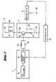
- the system comprises a fixed station 1 (constituting an active transponder) and a portable data transaction card 2 (constituting a passive transponder).
- the fixed station 1 comprises an rf oscillator 3 which generates a radio frequency signal which is fed to an amplifier detector 4 coupled to a resonant circuit 5 (constituting a station resonant circuit).
- the output from the amplifier detector 4 is fed to a band pass filter 6 and thence to a first microcomputer 7 (constituting a station data communications circuit).
- the microcomputer 7 is arranged to control the output from the rf oscillator 3 so that the effective frequency of the signal fed to the resonant circuit 5 may be altered.
- the portable data transaction card 2 comprises a resonant circuit 11 (constituting a card resonant circuit) whose output is fed to a rectifier 12 whose output is a dc voltage which provides power for the rest of the circuit.
- the resonant circuit 11 is also coupled to a loading circuit 14 connected to a data converter 15 whose output is fed to a data memory 16. Connected between the resonant circuit 11 and the data converter 15 is a reading circuit 17.
- the data converter 15 and the data memory 16 are preferably incorporated within a second microcomputer 18 and effectively constitute a card data communications circuit.
- the operation of the station 1 is as follows.
- the rf oscillator 3 generates an rf signal which is amplified by the amplifier detector 4.
- the resonant circuit 5 is tuned to the frequency of the rf oscillator 3 and has a high Q factor causing it to resonate when the input signal is at the desired frequency, but substantially to stop resonating when the rf frequency is changed by more than a predetermined amount.
- the function of the detector 4 is to detect a signal superimposed on the rf signal to which the resonant circuit 5 is tuned so that the rf signal can function as a carrier waveform which can be amplitude modulated by a suitable data signal generated within the data transaction card 2.
- the band pass filter 6 removes the rf component from the detected signal so that the original data signal may be processed and stored by the microcomputer 7.
- the microcomputer 7 provides means for adjusting the output frequency from the rf oscillator 3 so that the resultant shift in frequency is sufficient to prevent the resonant circuit 5 from resonating.
- the operation of the portable data transaction card 2 is as follows.
- the resonant circuit 11 is tuned to the same resonant frequency as that generated by the fixed station 1. Consequently, when the card 2 is brought close to the station 1 the card resonant circuit 11 starts to resonate and the resultant induced voltage is fed to the rectifier 12.
- the output from the rectifier 12 is a dc voltage which provides power for the communications circuitry associated with the card 2.
- the loading circuit 14 Immediately power is supplied to the card 2, the loading circuit 14 is activated in accordance with data stored in the data memory 16.
- the loading circuit 14 functions like a switch which, under normal conditions, generates a logic "1". By normal conditions is meant that the loading circuit 14 remains open and the resonant circuit 11 is therefore unloaded.
- the loading circuit 14 When the loading circuit 14 is activated, this loads the resonant circuit 11 thereby reducing its output and enabling transmission of logic "0".
- the loading circuit 14 must be repeatedly activated and deactivated in accordance with the data stored in the data memory 16. This is achieved by means of logic circuitry within the data converter 15 which, together with the loading circuit 14, constitutes modulating means for modulating the resonant frequency signal with the data signal generating within the card.
- the reading circuit 17 is designed to sense the condition of the resonant circuit 11 and functions like a JK flip-flop whose output toggles between logic "1" and "0" for each pulse of a clock input. By this means it is possible, as will be explained in greater detail with reference to Figs. 7, 8 and 9 below, to write data from the station 1 to the card 2.
- the rf oscillator 3 comprises a crystal oscillator 20 which generates an rf signal of characteristic frequency.
- the output from the crystal oscillator 20 is divided by a frequency divider 21 and the resulting lower frequency rf signal is fed to the base of a bipolar junction transistor 22.
- Coupling between the frequency divider 21 and the transistor 22 is afforded by means of a suitable impedance comprising a parallel connection of a resistor 23 and a capacitor 24.
- the value of this impedance is chosen to match the logic voltage levels of the frequency divider 21 to the analogue voltage levels of the transistor 22.
- the emitter of transistor 22 is connected to ground 26 via a parallel combination of a resistor 27 and a capacitor 28.
- Connected to the collector of transistor 22 is the cathode of a diode 29 whose anode is connected to a parallel combination of a coil 30 and a tuned capacitor 31 whose other ends are connected to the positive voltage rail 32.
- the inductance and variable capacitance of the coil 30 and the capacitor 31, respectively, are so chosen that the resultant tuned circuit will resonate at the frequency of the signal generated by the rf oscillator 3. It will thus be clear that the coil 30 and the capacitor 31 are equivalent to the station resonant circuit 5 shown in Fig. 1.
- the diode 29 functions as a buffer between the transistor 22 and the resonant circuit 5 and prevents the transistor 22 in the cut-off mode from loading the resonant circuit 5 and inhibiting oscillation.
- the combination of transistor 22, resistor 27, capacitor 28 and diode 29 func tions as the amplifier detector 4 shown functionally in Fig. 1.
- the voltage signal across the capacitor 28 is fed to the input of the band-pass filter 6 of known construction and is simply represented by a three terminal network (input, output and ground) in Fig. 2.
- the output from the band-pass filter 6 is fed to the microcomputer 7.
- the microcomputer 7 is arranged to alter the division ratio of the frequency divider 21 so that, under microcomputer control, the frequency of the signal generated by the rf oscillator 3 may be sufficiently changed to prevent the resonant circuit 5 from resonating.
- the card resonant circuit 11 comprises the centre-tapped coil 35 whose centre tap is connected to ground 26 and whose ends are connected to terminals 36 and 37 across which is connected a capacitor 38.
- the outputs from terminals 36 and 37 are fed, respectively, to the anodes of rectifier diodes 40 and 41.
- the cathodes of the rectifier diodes 40 and 41 are connected to a common terminal 42 which constitutes a positive voltage rail from which the card circuitry is powered.
- Connected between the positive voltage rail 42 and ground 26 is a smoothing capacitor 43 which reduces the ripple content of the rectified dc voltage signal.
- the combination of the rectifier diodes 40 and 41, together with the smoothing capacitor 43 constitutes the rectifier 12 shown functional ly in Fig. 1.
- Terminals 36 and 37 are also connected to the anodes of rectifier diodes 45 and 46, respectively, as well as to the anodes of rectifier diodes 47 and 48, respectively.
- the cathodes of diodes 45 and 46 are commonly connected to the input of the data converter 15.
- the diodes 45 and 46 constitute the loading circuit 14 shown functionally in Fig. 1.
- the cathodes of diodes 47 and 48 are commonly connected to a timing circuit comprising a capacitor 49 in parallel with a resistor 50 whose low voltage terminals are connected to ground 26.
- the combination of diodes 47 and 48, capacitor 49 and resistor 50 constitutes the reading circuit 17 shown functionally in Fig. 1 and whose output is fed to the data converter 15. It will be understood that whilst the reading circuit 17 may be built using discrete circuits, preferably the timing circuit comprising the capacitor 49 and the resistor 50 is included within the second microcomputer 18 constituting the card data communications circuit.
- the data transaction card 2 does not have its own power source but, rather, is powered by a voltage signal radiated by the station 1.
- the manner in which this is achieved is as follows.
- the card resonant circuit 11 starts to resonate when it is brought within a predetermined distance of the station resonant circuit 5 when the latter generates substantially the same frequency to which the card resonant circuit 11 is tuned.
- the magnitude of the voltage signal generated by the card resonant circuit 11 is a function of the distance between the station 1 and the card 2. In other words, the closer the card 2 is to the station 1 the greater will be the magnitude of the voltage signal induced in the card resonant circuit 11.
- the amplitude of the voltage signal may be varied up to 10V when the distance between the card 2 and the station 1 is 10 cm, according to the magnitude of the mutual coupling between the station 1 and the card 2.
- a zener diode (not shown) is used to clip the voltage to a safe level.
- Fig. 4 shows the form of the smoothed dc output generated by the rectifier 12.
- Fig. 5 shows graphically the form of the voltage-reactance characteristic for the station resonant circuit 5.
- the characteristic curve is substantially parabolic in shape, with a peak voltage corresponding to the resonant frequency f 0.
- the reactance of the resonant circuit 5 will change correspondingly and the resonant circuit voltage will fall. It will be seen that on either side of the peak voltage of the voltage-reactance characteristic there is a substantially linear portion wherein, for a small change in the reactance of the resonant circuit, there is a correspondingly larger change in the voltage developed by the resonant circuit 5.
- Figs. 6a, 6b and 6c illustrate the protocol according to which data is transmitted by the card 2.
- the data transmission pulses are of a standard pulse width which, for both logic “0" and “1", starts with a low voltage and ends at a high voltage.
- Fig. 6a shows the pulse shape for logic "0". In this case, the pulse voltage remains low twice as long as it remains high.
- Fig. 6b shows the opposite situation corresponding to logic "1".
- the pulse voltage remains high twice as long as it remains low.
- Fig. 6c shows the form of the pulse train which would be generated in order to transmit 001 (binary). With no data being transmitted, the voltage is high and falls as soon as the first pulse (corresponding to logic "0") is transmitted.
- the pulse period be represented by T
- the voltage remains low for 2/3T and then goes high for the remainder of the pulse period. It then falls for a further time 2/3T and rises for the rest of the second pulse period, corresponding to the transmission of a second logic "0". It then falls for a time of 1/3T and remains high for the rest of the pulse period, corresponding to the transmission of logic "1".
- Fig. 7 shows the voltage-frequency characteristic of the station resonant circuit 5.
- the shape of the curve is substantially parabolic with a peak voltage corresponding to the resonant frequency of the circuit, represented by f 0 in the diagram.
- f 0 the resonant frequency of the circuit
- the resonant circuit voltage will fall.
- Fig. 7 Depicted in Fig. 7 is a cut-off frequency ⁇ f such that at a frequency of f 0 ⁇ ⁇ f the voltage generated by the station resonant circuit 5 is insufficient to cause the card resonant circuit 11 to resonate.
- a control signal from the microcomputer 7 so alters the frequency-division ratio of the frequency divider circuit 21 (shown in Fig. 2) that the station resonant circuit 5 substantially ceases to resonate, as explained with reference to Fig. 7 above.
- the smoothing capacitor 43 within the rectifier 12 of the card 2 (see Fig. 3) and also the capacitor 49 within the timing circuit within the reading circuit 17 of the card 2 (as shown in Fig. 3) both start to discharge at rates determined by the time constants of the two circuits.
- the value of the smoothing capacitor 43 is chosen to be so much larger than that of capacitor 49 that capacitor 49 may substantially discharge while there still remains sufficient voltage across the smoothing capacitor 43 of the rectifier 12 to continue supplying power to the data communications circuitry provided within the data transaction card 2.
- the station resonant circuit 5 will re-continue to resonate and, by mutual coupling, so will the card resonant circuit 11.
- the speed with which the station resonant circuit 5 is disabled and re-enabled is thus arranged to be sufficiently fast that the transfer of dc power to the card 2 is not interrupted.
- the capacitor 49 within the reading circuit 17 is recharged through the diodes 47 and 48. Since these diodes have very low forward resistance, the capacitor 49 almost instantaneously recharges.
- Fig. 8a shows the discharge-recharge characteristic of capacitor 49 for an input signal V in corresponding to two control signals transmitted by the station microcomputer 7 to the frequency divider circuit 21 within the rf oscillator 3.
- Fig. 8b shows the corresponding signal V out generated by the data converter 15 within the card 2. It will be seen from Fig. 8b that the state of V out (i.e. high or low) changes each time the capacitor 49 is recharged. Thus, by altering the time interval between which the capa citor 49 is arranged to discharge and subsequently recharge, the pulse width of V out may be adjusted correspondingly.
- V out may be interpreted as a serial pulse train corresponding to a combination of logic "0"s and "1"s transmitted by the station 1.
- Figs. 9a and 9b illustrate this concept in more detail.
- Fig. 9a shows the voltage waveform V in developed across the capacitor 49 in Fig. 3 for transmitting the data 56 HEX from the station 1 to the card 2.
- the data corresponding to 01010110 (binary) is transmitted as a serial pulse train delimited by suitable start and stop bits. With no data being transmitted, V out is at an initial high voltage level which falls to a low voltage level corresponding to the transmission of the start bit. At the end of the data transmission, the voltage level of V out returns to, and remains at, its initial high voltage level to indicate the termination of data transmission. Comparing Fig. 9a with Fig.
- an access code may be pre-stored within the card memory so as to permit restricted access to the bearer of the card dependent on the particular code stored therein.
- the invention may also be utilized within a manufacturing system in which each workpiece carries an identity tag corresponding to the data card of the invention.
- the identity tag not only identifies the workpiece, but also permits a record of each machining operation, for example, to be written to the identity tag so that it contains an up-to-date record of all operations performed on the workpiece.
- the invention may also be employed as an automatic personnel time card or as a system for automatic debiting of a telephone subscriber's account, in which public telephones are adapted to read an account number from a data card carried by the subscriber, thereby obviating the need for regular subscribers to carry telephone tokens, pre-paid telephone cards and so on.
Landscapes
- Engineering & Computer Science (AREA)
- Artificial Intelligence (AREA)
- Computer Vision & Pattern Recognition (AREA)
- Physics & Mathematics (AREA)
- General Physics & Mathematics (AREA)
- Theoretical Computer Science (AREA)
- Near-Field Transmission Systems (AREA)
Applications Claiming Priority (2)
| Application Number | Priority Date | Filing Date | Title |
|---|---|---|---|
| IL82025A IL82025A (en) | 1987-03-27 | 1987-03-27 | Electronic data communications system |
| IL82025 | 1987-03-27 |
Publications (2)
| Publication Number | Publication Date |
|---|---|
| EP0289136A2 true EP0289136A2 (fr) | 1988-11-02 |
| EP0289136A3 EP0289136A3 (fr) | 1990-03-07 |
Family
ID=11057658
Family Applications (1)
| Application Number | Title | Priority Date | Filing Date |
|---|---|---|---|
| EP88302715A Withdrawn EP0289136A3 (fr) | 1987-03-27 | 1988-03-25 | Système électronique de communication de données |
Country Status (14)
| Country | Link |
|---|---|
| US (1) | US4814595A (fr) |
| EP (1) | EP0289136A3 (fr) |
| JP (1) | JPS643787A (fr) |
| AU (1) | AU1377688A (fr) |
| BR (1) | BR8801379A (fr) |
| DD (1) | DD269478A5 (fr) |
| DK (1) | DK167888A (fr) |
| FI (1) | FI881423A (fr) |
| HU (1) | HUT49764A (fr) |
| IL (1) | IL82025A (fr) |
| MX (1) | MX169307B (fr) |
| NO (1) | NO881341L (fr) |
| PT (1) | PT87089B (fr) |
| ZA (1) | ZA882160B (fr) |
Cited By (20)
| Publication number | Priority date | Publication date | Assignee | Title |
|---|---|---|---|---|
| EP0374018A1 (fr) * | 1988-12-16 | 1990-06-20 | France Telecom | Dispositif pour l'échange d'informations à distance entre un objet portatif et une station |
| WO1990009707A1 (fr) * | 1989-02-17 | 1990-08-23 | Integrated Silicon Design Pty. Ltd. | Systeme de repondeur |
| EP0460885A2 (fr) * | 1990-06-05 | 1991-12-11 | Hitachi Maxell Ltd. | Support d'enregistrement IC sans contact |
| EP0474286A2 (fr) * | 1990-09-03 | 1992-03-11 | Koninklijke Philips Electronics N.V. | Système d'échange d'information comportant un support d'informations et une unité de lecture et d'écriture |
| EP0492569A2 (fr) * | 1990-12-28 | 1992-07-01 | On Track Innovations Ltd. | Système et méthode pour la transmission de données sans contact |
| EP0518329A2 (fr) * | 1991-06-13 | 1992-12-16 | Siemens Aktiengesellschaft | Circuit pour la transmission sans contact d'énergie et de données à l'aide d'une tension alternative et d'un coupleur inductive |
| US5227779A (en) * | 1989-03-09 | 1993-07-13 | Cotag International Limited | Codable electronic devices |
| EP0576100A1 (fr) * | 1992-06-24 | 1993-12-29 | N.V. Nederlandsche Apparatenfabriek NEDAP | Système d'identification à haute fréquence résistant aux perturbations et ayant une grande distance de détection |
| EP0589046A1 (fr) * | 1992-02-18 | 1994-03-30 | Citizen Watch Co. Ltd. | Systeme porteur de donnees |
| EP0596124A1 (fr) † | 1991-12-04 | 1994-05-11 | Citizen Watch Co. Ltd. | Support de donnees |
| EP0602449A2 (fr) * | 1992-12-18 | 1994-06-22 | TEMIC TELEFUNKEN microelectronic GmbH | Carte avec IC |
| EP0746824A1 (fr) * | 1992-11-10 | 1996-12-11 | Xicor, Inc | Systeme d'alimentation et de communication sans fil communiquant des donnees entre un systeme central et un dispositif autonome |
| EP0810540A2 (fr) * | 1996-05-30 | 1997-12-03 | Motorola, Inc. | Système d'identification sans contact |
| NL1006493C2 (nl) * | 1997-07-04 | 1999-01-05 | Hedon Electronic Developments | Systeem voor het contactloos elektronisch uitwisselen van gegevens, alsmede lees/schrijfeenheid en drager bestemd voor toepassing in een dergelijk systeem. |
| WO2000052636A2 (fr) * | 1999-03-02 | 2000-09-08 | Konisa Limited | Systeme d'identification |
| US6252823B1 (en) | 1994-12-16 | 2001-06-26 | Vu-Data Limited | Recorder device, reading device and regulating device |
| EP0689149B1 (fr) * | 1994-06-21 | 2001-08-22 | Sony Chemicals Corporation | Cartes d'information sans contact |
| US6321067B1 (en) | 1996-09-13 | 2001-11-20 | Hitachi, Ltd. | Power transmission system IC card and information communication system using IC card |
| EP1231557A2 (fr) * | 2001-02-08 | 2002-08-14 | Fujitsu Limited | Appareil de traitement d'information et appareil de traitement d'information en forme de carte |
| EP1244175A1 (fr) * | 2001-03-20 | 2002-09-25 | Valeo Electronique | Antenne à spires émettrices de signaux dans une bande déterminée de fréquences |
Families Citing this family (53)
| Publication number | Priority date | Publication date | Assignee | Title |
|---|---|---|---|---|
| DE3810702A1 (de) * | 1988-03-25 | 1989-10-12 | Angewandte Digital Elektronik | Phasenstabilisierter, -gekoppelter schwingkreis |
| US5184001A (en) * | 1988-12-16 | 1993-02-02 | L'etat Francais Represente Par Le Ministre Des Postes, Des Telecommunications Et De L'espace (Centre National D'etudes Des Telecommunications) | System for remote information interchange between a portable object and a station |
| JPH03171384A (ja) * | 1989-11-30 | 1991-07-24 | Sony Corp | 情報読取装置 |
| JPH03189786A (ja) * | 1989-12-19 | 1991-08-19 | Sony Corp | 情報カード装置 |
| JP2543235B2 (ja) * | 1990-06-29 | 1996-10-16 | 松下電器産業株式会社 | Icカ―ドアダプタ |
| JPH0478985A (ja) * | 1990-07-23 | 1992-03-12 | Okamoto Kosaku Kikai Seisakusho:Kk | 情報記憶再生装置 |
| US5418353A (en) * | 1991-07-23 | 1995-05-23 | Hitachi Maxell, Ltd. | Non-contact, electromagnetically coupled transmission and receiving system for IC cards |
| EP0525642B1 (fr) * | 1991-07-23 | 1999-10-06 | Hitachi Maxell Ltd. | Système de lecture/écriture pour moyen d'enregistrement et système de carte à puce de non-contact |
| US5229652A (en) * | 1992-04-20 | 1993-07-20 | Hough Wayne E | Non-contact data and power connector for computer based modules |
| DE4327642C2 (de) * | 1993-05-17 | 1998-09-24 | Anatoli Stobbe | Lesegerät für ein Detektierplättchen |
| US5382780A (en) * | 1993-10-01 | 1995-01-17 | Duncan Industries Parking Control Systems Corp. | Portable time metering device |
| JPH0962816A (ja) * | 1994-10-06 | 1997-03-07 | Mitsubishi Electric Corp | 非接触icカードおよびこれを含む非接触icカードシステム |
| DE19500805C2 (de) * | 1995-01-13 | 2002-11-21 | Adp Gauselmann Gmbh | Datenübertragung zwischen einem Schreib-Lese-Gerät und einer batterielosen Chipkarte |
| JPH0981701A (ja) * | 1995-09-19 | 1997-03-28 | Toshiba Corp | 非接触式情報記録媒体および非接触式情報伝送方法 |
| US6249233B1 (en) | 1996-07-29 | 2001-06-19 | Baran Advanced Technologies (86) Ltd. | Vehicle parking system |
| IL116336A (en) | 1995-10-06 | 1998-09-24 | Baran Advanced Tech Ltd | Car parking system |
| US6010074A (en) * | 1996-04-01 | 2000-01-04 | Cubic Corporation | Contactless proximity automated data collection system and method with collision resolution |
| JP3392016B2 (ja) * | 1996-09-13 | 2003-03-31 | 株式会社日立製作所 | 電力伝送システム並びに電力伝送および情報通信システム |
| US5815020A (en) * | 1996-09-24 | 1998-09-29 | Motorola, Inc. | Balance differential receiver |
| US5812942A (en) * | 1996-09-24 | 1998-09-22 | Motorola, Inc. | Balanced differential radio receiver and method of operation |
| JPH10135882A (ja) * | 1996-10-24 | 1998-05-22 | Toshiba Corp | 非接触式情報記録媒体及びそのデータ送信方式 |
| JP3642124B2 (ja) * | 1996-11-08 | 2005-04-27 | 株式会社デンソー | 光学式読取装置および置き台 |
| IL120675A0 (en) * | 1997-04-15 | 1997-08-14 | Zuta Marc | Smart card device and method |
| JP3475996B2 (ja) * | 1997-10-07 | 2003-12-10 | インターナショナル・ビジネス・マシーンズ・コーポレーション | 非接触icカードシステム、icカード用のカードリーダ及びicカード |
| FR2780221B1 (fr) | 1998-06-22 | 2000-09-29 | Sgs Thomson Microelectronics | Emission d'une consigne de fonctionnement par une ligne d'alimentation alternative |
| FR2780220A1 (fr) | 1998-06-22 | 1999-12-24 | Sgs Thomson Microelectronics | Transmission de donnees numeriques sur une ligne d'alimentation alternative |
| JP3916328B2 (ja) * | 1998-07-27 | 2007-05-16 | ローム株式会社 | 非接触通信システム |
| KR20010075032A (ko) * | 1998-09-11 | 2001-08-09 | 비센트 비.인그라시아, 알크 엠 아헨 | 비접촉 프로그래밍이 가능한 정전 무선 주파수 식별 시스템 |
| US6650226B1 (en) | 1999-04-07 | 2003-11-18 | Stmicroelectronics S.A. | Detection, by an electromagnetic transponder reader, of the distance separating it from a transponder |
| FR2792134B1 (fr) * | 1999-04-07 | 2001-06-22 | St Microelectronics Sa | Detection de distance entre un transpondeur electromagnetique et une borne |
| FR2792130B1 (fr) | 1999-04-07 | 2001-11-16 | St Microelectronics Sa | Transpondeur electromagnetique a fonctionnement en couplage tres proche |
| FR2792136B1 (fr) | 1999-04-07 | 2001-11-16 | St Microelectronics Sa | Transmission en duplex dans un systeme de transpondeurs electromagnetiques |
| FR2792132B1 (fr) | 1999-04-07 | 2001-11-02 | St Microelectronics Sa | Borne de lecture d'un transpondeur electromagnetique fonctionnant en couplage tres proche |
| FR2792135B1 (fr) | 1999-04-07 | 2001-11-02 | St Microelectronics Sa | Fonctionnement en complage tres proche d'un systeme a transpondeur electromagnetique |
| FR2796781A1 (fr) | 1999-07-20 | 2001-01-26 | St Microelectronics Sa | Dimensionnement d'un systeme a transpondeur electromagnetique pour un fonctionnement en hyperproximite |
| US7049935B1 (en) | 1999-07-20 | 2006-05-23 | Stmicroelectronics S.A. | Sizing of an electromagnetic transponder system for a dedicated distant coupling operation |
| US7395960B1 (en) * | 2000-01-12 | 2008-07-08 | Memory Medallion, Inc. | System and method for delivering information at remote locations |
| FR2804557B1 (fr) * | 2000-01-31 | 2003-06-27 | St Microelectronics Sa | Adaptation de la puissance d'emission d'un lecteur de transpondeur electromagnetique |
| FR2808945B1 (fr) * | 2000-05-12 | 2002-08-16 | St Microelectronics Sa | Evaluation du nombre de transpondeurs electromagnetiques dans le champ d'un lecteur |
| FR2808946A1 (fr) | 2000-05-12 | 2001-11-16 | St Microelectronics Sa | Validation de la presence d'un transpondeur electromagnetique dans le champ d'un lecteur |
| FR2808942B1 (fr) * | 2000-05-12 | 2002-08-16 | St Microelectronics Sa | Validation de la presence d'un transpondeur electromagnetique dans le champ d'un lecteur a demodulation de phase |
| FR2808941B1 (fr) | 2000-05-12 | 2002-08-16 | St Microelectronics Sa | Validation de la presence d'un transpondeur electromagnetique dans le champ d'un lecteur a demodulation d'amplitude |
| FR2809235A1 (fr) * | 2000-05-17 | 2001-11-23 | St Microelectronics Sa | Antenne de generation d'un champ electromagnetique pour transpondeur |
| FR2809251B1 (fr) * | 2000-05-17 | 2003-08-15 | St Microelectronics Sa | Dispositif de production d'un champ electromagnetique pour transpondeur |
| US7055752B2 (en) * | 2000-05-22 | 2006-06-06 | Matsushita Electric Industrial Co., Ltd. | IC card |
| FR2812986B1 (fr) * | 2000-08-09 | 2002-10-31 | St Microelectronics Sa | Detection d'une signature electrique d'un transpondeur electromagnetique |
| US20030169169A1 (en) * | 2000-08-17 | 2003-09-11 | Luc Wuidart | Antenna generating an electromagnetic field for transponder |
| TW543894U (en) * | 2001-11-09 | 2003-07-21 | Holtek Semiconductor Inc | Signal receiving and transmitting device |
| DE10202304A1 (de) * | 2002-01-22 | 2003-07-31 | Fraunhofer Ges Forschung | Kryospeichereinrichtung mit Transponder |
| US7545272B2 (en) | 2005-02-08 | 2009-06-09 | Therasense, Inc. | RF tag on test strips, test strip vials and boxes |
| US20070087838A1 (en) * | 2005-09-12 | 2007-04-19 | Jonathan Bradbury | Video game media |
| US7883420B2 (en) * | 2005-09-12 | 2011-02-08 | Mattel, Inc. | Video game systems |
| US20070087837A1 (en) * | 2005-09-12 | 2007-04-19 | Jonathan Bradbury | Video game consoles |
Citations (2)
| Publication number | Priority date | Publication date | Assignee | Title |
|---|---|---|---|---|
| DE3242551A1 (de) * | 1981-11-17 | 1983-05-26 | Götting KG, 3161 Röddensen | Anordnung zum identifizieren eines objektes |
| WO1986001058A1 (fr) * | 1984-07-26 | 1986-02-13 | Robert Bosch Gmbh | Installation pour le transfert de donnees binaires entre un support d'information mobile et une station fixe |
Family Cites Families (1)
| Publication number | Priority date | Publication date | Assignee | Title |
|---|---|---|---|---|
| JPH0734215B2 (ja) * | 1985-02-27 | 1995-04-12 | 株式会社日立製作所 | Icカ−ド |
-
1987
- 1987-03-27 IL IL82025A patent/IL82025A/xx not_active IP Right Cessation
-
1988
- 1988-03-24 FI FI881423A patent/FI881423A/fi not_active IP Right Cessation
- 1988-03-25 MX MX010884A patent/MX169307B/es unknown
- 1988-03-25 ZA ZA882160A patent/ZA882160B/xx unknown
- 1988-03-25 EP EP88302715A patent/EP0289136A3/fr not_active Withdrawn
- 1988-03-25 NO NO881341A patent/NO881341L/no unknown
- 1988-03-25 DD DD88314037A patent/DD269478A5/de unknown
- 1988-03-25 DK DK167888A patent/DK167888A/da active IP Right Grant
- 1988-03-25 HU HU881527A patent/HUT49764A/hu unknown
- 1988-03-25 BR BR8801379A patent/BR8801379A/pt unknown
- 1988-03-25 PT PT87089A patent/PT87089B/pt not_active IP Right Cessation
- 1988-03-28 AU AU13776/88A patent/AU1377688A/en not_active Abandoned
- 1988-03-28 JP JP63072158A patent/JPS643787A/ja active Pending
- 1988-03-28 US US07/174,224 patent/US4814595A/en not_active Expired - Fee Related
Patent Citations (2)
| Publication number | Priority date | Publication date | Assignee | Title |
|---|---|---|---|---|
| DE3242551A1 (de) * | 1981-11-17 | 1983-05-26 | Götting KG, 3161 Röddensen | Anordnung zum identifizieren eines objektes |
| WO1986001058A1 (fr) * | 1984-07-26 | 1986-02-13 | Robert Bosch Gmbh | Installation pour le transfert de donnees binaires entre un support d'information mobile et une station fixe |
Cited By (36)
| Publication number | Priority date | Publication date | Assignee | Title |
|---|---|---|---|---|
| FR2640830A1 (fr) * | 1988-12-16 | 1990-06-22 | Levionnais Philippe | Dispositif pour l'echange d'informations a distance entre un objet portatif et une station |
| EP0374018A1 (fr) * | 1988-12-16 | 1990-06-20 | France Telecom | Dispositif pour l'échange d'informations à distance entre un objet portatif et une station |
| WO1990009707A1 (fr) * | 1989-02-17 | 1990-08-23 | Integrated Silicon Design Pty. Ltd. | Systeme de repondeur |
| US5227779A (en) * | 1989-03-09 | 1993-07-13 | Cotag International Limited | Codable electronic devices |
| EP0460885A2 (fr) * | 1990-06-05 | 1991-12-11 | Hitachi Maxell Ltd. | Support d'enregistrement IC sans contact |
| US5353434A (en) * | 1990-06-05 | 1994-10-04 | Hitachi Maxell, Ltd. | Non-contact IC recording medium |
| EP0460885A3 (en) * | 1990-06-05 | 1993-03-31 | Hitachi Maxell Ltd. | Non-contact ic recording medium |
| EP0474286A2 (fr) * | 1990-09-03 | 1992-03-11 | Koninklijke Philips Electronics N.V. | Système d'échange d'information comportant un support d'informations et une unité de lecture et d'écriture |
| EP0474286A3 (fr) * | 1990-09-03 | 1994-04-20 | Philips Nv | |
| EP0492569A3 (en) * | 1990-12-28 | 1993-10-27 | On Track Innovations Ltd | A system and method for the non-contact transmission of data |
| EP0492569A2 (fr) * | 1990-12-28 | 1992-07-01 | On Track Innovations Ltd. | Système et méthode pour la transmission de données sans contact |
| EP0518329A3 (en) * | 1991-06-13 | 1993-06-16 | Siemens Aktiengesellschaft | Circuit arrangement for the contactless transmission of energy and data with the aid of an ac voltage and an inductive coupler |
| EP0518329A2 (fr) * | 1991-06-13 | 1992-12-16 | Siemens Aktiengesellschaft | Circuit pour la transmission sans contact d'énergie et de données à l'aide d'une tension alternative et d'un coupleur inductive |
| EP0596124A1 (fr) † | 1991-12-04 | 1994-05-11 | Citizen Watch Co. Ltd. | Support de donnees |
| EP0596124B2 (fr) † | 1991-12-04 | 2001-12-19 | Citizen Watch Co. Ltd. | Support de donnees |
| EP0589046A1 (fr) * | 1992-02-18 | 1994-03-30 | Citizen Watch Co. Ltd. | Systeme porteur de donnees |
| EP0589046A4 (fr) * | 1992-02-18 | 1994-10-19 | Citizen Watch Co Ltd | Systeme porteur de donnees. |
| US5570086A (en) * | 1992-02-18 | 1996-10-29 | Citizen Watch Co., Ltd. | Data carrier system |
| EP0576100A1 (fr) * | 1992-06-24 | 1993-12-29 | N.V. Nederlandsche Apparatenfabriek NEDAP | Système d'identification à haute fréquence résistant aux perturbations et ayant une grande distance de détection |
| EP0746824A1 (fr) * | 1992-11-10 | 1996-12-11 | Xicor, Inc | Systeme d'alimentation et de communication sans fil communiquant des donnees entre un systeme central et un dispositif autonome |
| EP0746824A4 (fr) * | 1992-11-10 | 1998-05-06 | Xicor Inc | Systeme d'alimentation et de communication sans fil communiquant des donnees entre un systeme central et un dispositif autonome |
| EP0602449A3 (fr) * | 1992-12-18 | 1994-10-19 | Telefunken Microelectron | Carte avec IC. |
| US5449894A (en) * | 1992-12-18 | 1995-09-12 | Temic Telefunken Microelectronic Gmbh | IC card having a voltage detector for detecting blanking gaps in an energy-transmitting alternating field |
| EP0602449A2 (fr) * | 1992-12-18 | 1994-06-22 | TEMIC TELEFUNKEN microelectronic GmbH | Carte avec IC |
| EP0689149B1 (fr) * | 1994-06-21 | 2001-08-22 | Sony Chemicals Corporation | Cartes d'information sans contact |
| US6252823B1 (en) | 1994-12-16 | 2001-06-26 | Vu-Data Limited | Recorder device, reading device and regulating device |
| EP0810540A2 (fr) * | 1996-05-30 | 1997-12-03 | Motorola, Inc. | Système d'identification sans contact |
| EP0810540A3 (fr) * | 1996-05-30 | 1999-01-20 | Motorola, Inc. | Système d'identification sans contact |
| US6321067B1 (en) | 1996-09-13 | 2001-11-20 | Hitachi, Ltd. | Power transmission system IC card and information communication system using IC card |
| NL1006493C2 (nl) * | 1997-07-04 | 1999-01-05 | Hedon Electronic Developments | Systeem voor het contactloos elektronisch uitwisselen van gegevens, alsmede lees/schrijfeenheid en drager bestemd voor toepassing in een dergelijk systeem. |
| WO2000052636A2 (fr) * | 1999-03-02 | 2000-09-08 | Konisa Limited | Systeme d'identification |
| WO2000052636A3 (fr) * | 1999-03-02 | 2001-01-25 | Konisa Ltd | Systeme d'identification |
| EP1231557A2 (fr) * | 2001-02-08 | 2002-08-14 | Fujitsu Limited | Appareil de traitement d'information et appareil de traitement d'information en forme de carte |
| EP1231557A3 (fr) * | 2001-02-08 | 2003-06-11 | Fujitsu Limited | Appareil de traitement d'information et appareil de traitement d'information en forme de carte |
| US7003680B2 (en) | 2001-02-08 | 2006-02-21 | Fujitsu Limited | Contactless apparatus and card-type device having clock rectifier that is independent of power rectifier and demodulator with RC time constant based on selectable resistor |
| EP1244175A1 (fr) * | 2001-03-20 | 2002-09-25 | Valeo Electronique | Antenne à spires émettrices de signaux dans une bande déterminée de fréquences |
Also Published As
| Publication number | Publication date |
|---|---|
| JPS643787A (en) | 1989-01-09 |
| EP0289136A3 (fr) | 1990-03-07 |
| HUT49764A (en) | 1989-10-30 |
| PT87089B (pt) | 1995-03-31 |
| NO881341L (no) | 1988-09-28 |
| IL82025A (en) | 1993-07-08 |
| DK167888D0 (da) | 1988-03-25 |
| US4814595A (en) | 1989-03-21 |
| FI881423A (fi) | 1988-09-28 |
| AU1377688A (en) | 1988-09-29 |
| DK167888A (da) | 1988-09-28 |
| ZA882160B (fr) | 1988-09-15 |
| PT87089A (pt) | 1989-03-30 |
| IL82025A0 (en) | 1987-10-20 |
| NO881341D0 (no) | 1988-03-25 |
| DD269478A5 (de) | 1989-06-28 |
| MX169307B (es) | 1993-06-29 |
| BR8801379A (pt) | 1988-11-01 |
| FI881423A0 (fi) | 1988-03-24 |
Similar Documents
| Publication | Publication Date | Title |
|---|---|---|
| US4814595A (en) | Electronic data communications system | |
| US5241160A (en) | System and method for the non-contact transmission of data | |
| EP0297688B1 (fr) | Dispositif d'identification électronique | |
| EP2327230B1 (fr) | Étiquette d'identification électronique bidirectionnelle simultanée et bidirectionnelle à l'alternat combinée | |
| US5652423A (en) | Non-contacting RF-ID card for wide voltage range input | |
| US5345231A (en) | Contactless inductive data-transmission system | |
| CA2318538C (fr) | Carte a memoire avec/sans contact pourvue d'une interface antenne personnalisable | |
| US4918416A (en) | Electronic proximity identification system | |
| EP0209588B1 (fr) | Systeme d'identification | |
| EP0267009B1 (fr) | Dispositifs de mémorisation de données | |
| EP0393089B1 (fr) | Repondeur | |
| US5499017A (en) | Multi-memory electronic identification tag | |
| EP1251452B1 (fr) | Etiquette d'identification électronique multimémoire | |
| CA1300686C (fr) | Systeme d'echange de donnees sans contact | |
| US5257011A (en) | Data altering means for multi-memory electronic identification tag | |
| US6650229B1 (en) | Electromagnetic transponder read terminal operating in very close coupling | |
| US5892300A (en) | System for contactless power and data transmission | |
| EP0492569B1 (fr) | Système et méthode pour la transmission de données sans contact | |
| JPH0720236A (ja) | トランスポンダ装置 | |
| EP0537378A1 (fr) | Méthode de lecture de données enregistrées dans un répondeur passif au moyen d'un dispositif d'interrogation comprenant une partie de réception | |
| US6118367A (en) | Data carrier system | |
| CA2272619A1 (fr) | Circuit de verrouillage a modulation compensee |
Legal Events
| Date | Code | Title | Description |
|---|---|---|---|
| PUAI | Public reference made under article 153(3) epc to a published international application that has entered the european phase |
Free format text: ORIGINAL CODE: 0009012 |
|
| AK | Designated contracting states |
Kind code of ref document: A2 Designated state(s): AT BE CH DE ES FR GB IT LI NL SE |
|
| PUAL | Search report despatched |
Free format text: ORIGINAL CODE: 0009013 |
|
| AK | Designated contracting states |
Kind code of ref document: A3 Designated state(s): AT BE CH DE ES FR GB IT LI NL SE |
|
| STAA | Information on the status of an ep patent application or granted ep patent |
Free format text: STATUS: THE APPLICATION IS DEEMED TO BE WITHDRAWN |
|
| 18D | Application deemed to be withdrawn |
Effective date: 19900908 |