EP0286258B1 - Cadre à contact hybride pour tête d'impression thermique à jet d'encre et ses procédé de fabrication et de connexion - Google Patents
Cadre à contact hybride pour tête d'impression thermique à jet d'encre et ses procédé de fabrication et de connexion Download PDFInfo
- Publication number
- EP0286258B1 EP0286258B1 EP88302408A EP88302408A EP0286258B1 EP 0286258 B1 EP0286258 B1 EP 0286258B1 EP 88302408 A EP88302408 A EP 88302408A EP 88302408 A EP88302408 A EP 88302408A EP 0286258 B1 EP0286258 B1 EP 0286258B1
- Authority
- EP
- European Patent Office
- Prior art keywords
- leads
- interconnect
- fingers
- contact
- lead frame
- Prior art date
- Legal status (The legal status is an assumption and is not a legal conclusion. Google has not performed a legal analysis and makes no representation as to the accuracy of the status listed.)
- Expired - Lifetime
Links
- 238000000034 method Methods 0.000 title claims description 24
- 238000004519 manufacturing process Methods 0.000 title description 11
- 239000000758 substrate Substances 0.000 claims description 20
- 239000004642 Polyimide Substances 0.000 claims description 18
- 229920001721 polyimide Polymers 0.000 claims description 18
- 239000002184 metal Substances 0.000 claims description 13
- 229910052751 metal Inorganic materials 0.000 claims description 13
- 230000033001 locomotion Effects 0.000 claims description 7
- 239000000853 adhesive Substances 0.000 claims description 6
- 230000001070 adhesive effect Effects 0.000 claims description 6
- 230000013011 mating Effects 0.000 claims description 5
- 229910000881 Cu alloy Inorganic materials 0.000 claims description 3
- 238000005452 bending Methods 0.000 claims description 3
- 239000010949 copper Substances 0.000 description 15
- 229920003223 poly(pyromellitimide-1,4-diphenyl ether) Polymers 0.000 description 15
- 239000010410 layer Substances 0.000 description 10
- 239000010409 thin film Substances 0.000 description 6
- 239000000523 sample Substances 0.000 description 5
- 238000013459 approach Methods 0.000 description 3
- 238000007641 inkjet printing Methods 0.000 description 3
- 239000000463 material Substances 0.000 description 3
- 229910000679 solder Inorganic materials 0.000 description 3
- 238000012360 testing method Methods 0.000 description 3
- 238000010276 construction Methods 0.000 description 2
- 238000011109 contamination Methods 0.000 description 2
- 238000005516 engineering process Methods 0.000 description 2
- 238000005530 etching Methods 0.000 description 2
- PCHJSUWPFVWCPO-UHFFFAOYSA-N gold Chemical compound [Au] PCHJSUWPFVWCPO-UHFFFAOYSA-N 0.000 description 2
- 239000010931 gold Substances 0.000 description 2
- 229910052737 gold Inorganic materials 0.000 description 2
- 239000011810 insulating material Substances 0.000 description 2
- 230000003647 oxidation Effects 0.000 description 2
- 238000007254 oxidation reaction Methods 0.000 description 2
- 239000004033 plastic Substances 0.000 description 2
- 229920003023 plastic Polymers 0.000 description 2
- 230000001681 protective effect Effects 0.000 description 2
- 230000002441 reversible effect Effects 0.000 description 2
- 230000002393 scratching effect Effects 0.000 description 2
- 229910021578 Iron(III) chloride Inorganic materials 0.000 description 1
- 239000012790 adhesive layer Substances 0.000 description 1
- 229910045601 alloy Inorganic materials 0.000 description 1
- 239000000956 alloy Substances 0.000 description 1
- DMFGNRRURHSENX-UHFFFAOYSA-N beryllium copper Chemical compound [Be].[Cu] DMFGNRRURHSENX-UHFFFAOYSA-N 0.000 description 1
- 239000011248 coating agent Substances 0.000 description 1
- 238000000576 coating method Methods 0.000 description 1
- 239000003086 colorant Substances 0.000 description 1
- 238000005260 corrosion Methods 0.000 description 1
- 230000007797 corrosion Effects 0.000 description 1
- 239000000835 fiber Substances 0.000 description 1
- 238000003780 insertion Methods 0.000 description 1
- 230000037431 insertion Effects 0.000 description 1
- 230000002452 interceptive effect Effects 0.000 description 1
- RBTARNINKXHZNM-UHFFFAOYSA-K iron trichloride Chemical compound Cl[Fe](Cl)Cl RBTARNINKXHZNM-UHFFFAOYSA-K 0.000 description 1
- 239000002648 laminated material Substances 0.000 description 1
- 238000010030 laminating Methods 0.000 description 1
- 238000003475 lamination Methods 0.000 description 1
- 239000000155 melt Substances 0.000 description 1
- 229910001092 metal group alloy Inorganic materials 0.000 description 1
- 238000012986 modification Methods 0.000 description 1
- 230000004048 modification Effects 0.000 description 1
- 230000002093 peripheral effect Effects 0.000 description 1
- 229920002120 photoresistant polymer Polymers 0.000 description 1
- 238000007747 plating Methods 0.000 description 1
- 230000002028 premature Effects 0.000 description 1
- 238000003825 pressing Methods 0.000 description 1
- 238000007639 printing Methods 0.000 description 1
- 238000012545 processing Methods 0.000 description 1
- 238000006748 scratching Methods 0.000 description 1
- 238000007789 sealing Methods 0.000 description 1
- 239000004065 semiconductor Substances 0.000 description 1
- 238000000926 separation method Methods 0.000 description 1
- 239000002356 single layer Substances 0.000 description 1
- 238000005476 soldering Methods 0.000 description 1
Images


Classifications
-
- H—ELECTRICITY
- H05—ELECTRIC TECHNIQUES NOT OTHERWISE PROVIDED FOR
- H05K—PRINTED CIRCUITS; CASINGS OR CONSTRUCTIONAL DETAILS OF ELECTRIC APPARATUS; MANUFACTURE OF ASSEMBLAGES OF ELECTRICAL COMPONENTS
- H05K3/00—Apparatus or processes for manufacturing printed circuits
- H05K3/40—Forming printed elements for providing electric connections to or between printed circuits
- H05K3/4092—Integral conductive tabs, i.e. conductive parts partly detached from the substrate
-
- B—PERFORMING OPERATIONS; TRANSPORTING
- B41—PRINTING; LINING MACHINES; TYPEWRITERS; STAMPS
- B41J—TYPEWRITERS; SELECTIVE PRINTING MECHANISMS, i.e. MECHANISMS PRINTING OTHERWISE THAN FROM A FORME; CORRECTION OF TYPOGRAPHICAL ERRORS
- B41J2/00—Typewriters or selective printing mechanisms characterised by the printing or marking process for which they are designed
- B41J2/005—Typewriters or selective printing mechanisms characterised by the printing or marking process for which they are designed characterised by bringing liquid or particles selectively into contact with a printing material
- B41J2/01—Ink jet
- B41J2/135—Nozzles
- B41J2/14—Structure thereof only for on-demand ink jet heads
- B41J2/14016—Structure of bubble jet print heads
- B41J2/14024—Assembling head parts
-
- B—PERFORMING OPERATIONS; TRANSPORTING
- B41—PRINTING; LINING MACHINES; TYPEWRITERS; STAMPS
- B41J—TYPEWRITERS; SELECTIVE PRINTING MECHANISMS, i.e. MECHANISMS PRINTING OTHERWISE THAN FROM A FORME; CORRECTION OF TYPOGRAPHICAL ERRORS
- B41J2/00—Typewriters or selective printing mechanisms characterised by the printing or marking process for which they are designed
- B41J2/005—Typewriters or selective printing mechanisms characterised by the printing or marking process for which they are designed characterised by bringing liquid or particles selectively into contact with a printing material
- B41J2/01—Ink jet
- B41J2/135—Nozzles
- B41J2/14—Structure thereof only for on-demand ink jet heads
- B41J2/14016—Structure of bubble jet print heads
- B41J2/14072—Electrical connections, e.g. details on electrodes, connecting the chip to the outside...
-
- B—PERFORMING OPERATIONS; TRANSPORTING
- B41—PRINTING; LINING MACHINES; TYPEWRITERS; STAMPS
- B41J—TYPEWRITERS; SELECTIVE PRINTING MECHANISMS, i.e. MECHANISMS PRINTING OTHERWISE THAN FROM A FORME; CORRECTION OF TYPOGRAPHICAL ERRORS
- B41J2/00—Typewriters or selective printing mechanisms characterised by the printing or marking process for which they are designed
- B41J2/005—Typewriters or selective printing mechanisms characterised by the printing or marking process for which they are designed characterised by bringing liquid or particles selectively into contact with a printing material
- B41J2/01—Ink jet
- B41J2/135—Nozzles
- B41J2/16—Production of nozzles
- B41J2/1601—Production of bubble jet print heads
- B41J2/1603—Production of bubble jet print heads of the front shooter type
-
- B—PERFORMING OPERATIONS; TRANSPORTING
- B41—PRINTING; LINING MACHINES; TYPEWRITERS; STAMPS
- B41J—TYPEWRITERS; SELECTIVE PRINTING MECHANISMS, i.e. MECHANISMS PRINTING OTHERWISE THAN FROM A FORME; CORRECTION OF TYPOGRAPHICAL ERRORS
- B41J2/00—Typewriters or selective printing mechanisms characterised by the printing or marking process for which they are designed
- B41J2/005—Typewriters or selective printing mechanisms characterised by the printing or marking process for which they are designed characterised by bringing liquid or particles selectively into contact with a printing material
- B41J2/01—Ink jet
- B41J2/135—Nozzles
- B41J2/16—Production of nozzles
- B41J2/1621—Manufacturing processes
- B41J2/1626—Manufacturing processes etching
- B41J2/1629—Manufacturing processes etching wet etching
-
- B—PERFORMING OPERATIONS; TRANSPORTING
- B41—PRINTING; LINING MACHINES; TYPEWRITERS; STAMPS
- B41J—TYPEWRITERS; SELECTIVE PRINTING MECHANISMS, i.e. MECHANISMS PRINTING OTHERWISE THAN FROM A FORME; CORRECTION OF TYPOGRAPHICAL ERRORS
- B41J2/00—Typewriters or selective printing mechanisms characterised by the printing or marking process for which they are designed
- B41J2/005—Typewriters or selective printing mechanisms characterised by the printing or marking process for which they are designed characterised by bringing liquid or particles selectively into contact with a printing material
- B41J2/01—Ink jet
- B41J2/135—Nozzles
- B41J2/16—Production of nozzles
- B41J2/1621—Manufacturing processes
- B41J2/1632—Manufacturing processes machining
-
- B—PERFORMING OPERATIONS; TRANSPORTING
- B41—PRINTING; LINING MACHINES; TYPEWRITERS; STAMPS
- B41J—TYPEWRITERS; SELECTIVE PRINTING MECHANISMS, i.e. MECHANISMS PRINTING OTHERWISE THAN FROM A FORME; CORRECTION OF TYPOGRAPHICAL ERRORS
- B41J2/00—Typewriters or selective printing mechanisms characterised by the printing or marking process for which they are designed
- B41J2/005—Typewriters or selective printing mechanisms characterised by the printing or marking process for which they are designed characterised by bringing liquid or particles selectively into contact with a printing material
- B41J2/01—Ink jet
- B41J2/135—Nozzles
- B41J2/16—Production of nozzles
- B41J2/1621—Manufacturing processes
- B41J2/164—Manufacturing processes thin film formation
-
- B—PERFORMING OPERATIONS; TRANSPORTING
- B41—PRINTING; LINING MACHINES; TYPEWRITERS; STAMPS
- B41J—TYPEWRITERS; SELECTIVE PRINTING MECHANISMS, i.e. MECHANISMS PRINTING OTHERWISE THAN FROM A FORME; CORRECTION OF TYPOGRAPHICAL ERRORS
- B41J29/00—Details of, or accessories for, typewriters or selective printing mechanisms not otherwise provided for
-
- B—PERFORMING OPERATIONS; TRANSPORTING
- B41—PRINTING; LINING MACHINES; TYPEWRITERS; STAMPS
- B41J—TYPEWRITERS; SELECTIVE PRINTING MECHANISMS, i.e. MECHANISMS PRINTING OTHERWISE THAN FROM A FORME; CORRECTION OF TYPOGRAPHICAL ERRORS
- B41J2/00—Typewriters or selective printing mechanisms characterised by the printing or marking process for which they are designed
- B41J2/005—Typewriters or selective printing mechanisms characterised by the printing or marking process for which they are designed characterised by bringing liquid or particles selectively into contact with a printing material
- B41J2/01—Ink jet
- B41J2/135—Nozzles
- B41J2/14—Structure thereof only for on-demand ink jet heads
- B41J2002/14362—Assembling elements of heads
-
- H—ELECTRICITY
- H05—ELECTRIC TECHNIQUES NOT OTHERWISE PROVIDED FOR
- H05K—PRINTED CIRCUITS; CASINGS OR CONSTRUCTIONAL DETAILS OF ELECTRIC APPARATUS; MANUFACTURE OF ASSEMBLAGES OF ELECTRICAL COMPONENTS
- H05K1/00—Printed circuits
- H05K1/02—Details
- H05K1/09—Use of materials for the conductive, e.g. metallic pattern
-
- Y—GENERAL TAGGING OF NEW TECHNOLOGICAL DEVELOPMENTS; GENERAL TAGGING OF CROSS-SECTIONAL TECHNOLOGIES SPANNING OVER SEVERAL SECTIONS OF THE IPC; TECHNICAL SUBJECTS COVERED BY FORMER USPC CROSS-REFERENCE ART COLLECTIONS [XRACs] AND DIGESTS
- Y10—TECHNICAL SUBJECTS COVERED BY FORMER USPC
- Y10T—TECHNICAL SUBJECTS COVERED BY FORMER US CLASSIFICATION
- Y10T29/00—Metal working
- Y10T29/49—Method of mechanical manufacture
- Y10T29/49002—Electrical device making
- Y10T29/49082—Resistor making
- Y10T29/49083—Heater type
-
- Y—GENERAL TAGGING OF NEW TECHNOLOGICAL DEVELOPMENTS; GENERAL TAGGING OF CROSS-SECTIONAL TECHNOLOGIES SPANNING OVER SEVERAL SECTIONS OF THE IPC; TECHNICAL SUBJECTS COVERED BY FORMER USPC CROSS-REFERENCE ART COLLECTIONS [XRACs] AND DIGESTS
- Y10—TECHNICAL SUBJECTS COVERED BY FORMER USPC
- Y10T—TECHNICAL SUBJECTS COVERED BY FORMER US CLASSIFICATION
- Y10T29/00—Metal working
- Y10T29/49—Method of mechanical manufacture
- Y10T29/49002—Electrical device making
- Y10T29/49082—Resistor making
- Y10T29/49099—Coating resistive material on a base
-
- Y—GENERAL TAGGING OF NEW TECHNOLOGICAL DEVELOPMENTS; GENERAL TAGGING OF CROSS-SECTIONAL TECHNOLOGIES SPANNING OVER SEVERAL SECTIONS OF THE IPC; TECHNICAL SUBJECTS COVERED BY FORMER USPC CROSS-REFERENCE ART COLLECTIONS [XRACs] AND DIGESTS
- Y10—TECHNICAL SUBJECTS COVERED BY FORMER USPC
- Y10T—TECHNICAL SUBJECTS COVERED BY FORMER US CLASSIFICATION
- Y10T29/00—Metal working
- Y10T29/49—Method of mechanical manufacture
- Y10T29/49002—Electrical device making
- Y10T29/49117—Conductor or circuit manufacturing
- Y10T29/49121—Beam lead frame or beam lead device
Definitions
- the method of making the test probe as described in US 3803709 includes forming step shaped projections extending pyramidally downwardly in a generally flat array of leads.
- the outer ends of the leads are joined by expansion elements to accommodate lead movement as the projections are formed.
- the shaped leads are then embedded in material of fixed a plastics lead-support frame, and the expansion elements are removed to leave the ends of the leads electrically isolated.
- the lead frame itself includes a plurality of electrical contact areas at one location thereon, and these contact areas are electrically connected to the corresponding plurality of flexible leads at another location within the lead frame.
- these leads may be flexed and spring biased through the angle ⁇ to the plane of interconnection when receiving an electrical device in good compressive electrical contact, and the external contacts, the lead frame contacts, amd the contacts on the electrical device all lie substantially in a single plane of interconnection.
- a metal pattern is provided within a lead frame type structure and includes plurality of metal fingers or leads extending in parallel towards a central area within the lead frame.
- This interconnect circuit includes connection tips on the ends of these leads which define areas of connection to a corresponding plurality of mating contact pads on a thermal ink jet printhead. These fingers or leads further extend to a remote area of the lead frame and terminate at a plurality of electrical contact areas to which flex circuits or printed circuits may be connected.
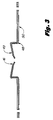
- Figure 1A is an isometric view of the hybrid interconnect lead frame according to the invention.
- Figure 1B is a greatly enlarged fragmented view of an end portion of the lead frame of Figure 1A and illustrating the path of the conductive leads extending through outer insulating material.
- Figure 1C is an enlarged view of the end portions of the leads and contact areas in Figure 1A.
- Figure 1D is a cross section view of an alternative contact tip construction for the lead frame according to the invention.
- Figure 2 is an isometric view of the lead frame of Figure 1A and showing its mating spatial relationship to a thermal ink jet printhead prior to electrical interconnection of these two members.
- Figure 3 is a cross section view taken along lines 3-3 of Figure 2.
- Figure 4 is an isometric view similar to Figure 2 and taken after insertion of the printhead into the printhead carriage where it makes electrical interconnection to the lead frame member.
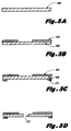
- FIGS 5A through 5F illustrate the process sequence used to make the lead frame interconnect circuit construction thereof along the interior portions of the lead frame in the cross section of lines 5-5 of Figure 4.
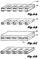
- Figures 6A-6D illustrate a process sequence corresponding to Figures 5A-5D and taken along portions of the lead frame in the plane of lines 6-6 of Figure 4.
- Figure 7 is a schematic view of the lead frame, in contact with the ink jet printhead in its in-carriage print position and making electrical interconnection between the printhead and a flexible (flex) circuit.
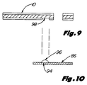
- Figure 8 shows the spatial relationship between the lead frame and the flex circuit to which it connects.
- Figure 9 is a cross section view taken along lines 9-9 of Figure 8.
- Figure 10 is a cross section view taken along lines 10-10 of Figure 8.
- the hybrid interconnect lead frame 10 includes an outer frame member 12 of rectangular geometry and surrounding a plurality of laminated flexible lead members 14 which extend as shown at an angle ⁇ into a central region of the frame.
- the tips 16 of the individual flexible leads are exposed for spring biased electrical connection to an ink jet printhead as will be further described.
- the tips 16 of the leads extending from opposite ends of the frame 10 are separated by a dimension indicated as 18 which corresponds to the width dimension of a thermal ink jet printhead. Electrical contact pads of this printhead will make contact with the tips 16 of the leads as these leads are moved through the angle ⁇ of approximately 15° and to the plane of interconnection with the printhead.
- the individual leads 14 are insulated one from another by the polyimide and extend between the two layers of polyimide through regions 31, 32 and terminate at exposed contact pads 33, 34 which are located adjacent the rectangular slots 28 and 30. This is illustrated in Figure 1B, in which the dashed lines indicate the presence of the BeCu leads and frame under the covering layer of polyimide. The leads 14 extend to the contact pads 33, 34 but are connected to the frame with polyimide only.
- the polyimide Kapton be sufficiently rigid so that it holds the lead fingers together and maintains a constant separation therebetween, while simultaneously allowing these fingers to flex independently of one another and to accomodate for differences in contact pad height, for example, produced by variations in manufacturing tolerances.
- FIG. 3 there is shown a cross section view of the hybrid interconnect lead frame taken along lines 3-3 of Figure 2.
- the exposed lead tips 16 extend toward the central area of the lead frame in the unbiased position and at an angle ⁇ with respect to the plane of interconnection as previously described.
- the Be.Cu alloy leads 48 are laminated on both sides, with the polyimide laminate Kapton 49 extending on the top surface of the leads to near the ends 16 thereof.
- This polyimide laminate material 50 on the lower surface of the Be.Cu lead 48 extends only to an area adjacent the L shaped bend thereof. This configuration is chosen because it is desirable to minimize the amount of polyimide in the bend area of the lead frame in order to improve bending tolerances.
- a single layer of polyimide in the region of the lead frame that flexes is typically an optimum amount for holding the leads together while still allowing them to flex somewhat independently.
- Figure 5A shows a cross section of the Be.Cu substrate 48 taken along the length dimension thereof.
- the substrate 48 is typically 0.15-0.2 ⁇ m (6-8 mils) in thickness and is provided with a Kapton protective and insulating polyimide layer 49 in the geometry shown in Figure 5B on the topside of the substrate 48.
- Another protective Kapton coating 50 is provided in the geometry shown in Figure 5C on the lower surface of the substrate 48.
- the Be.Cu substrate is then cut or etched in the center thereof as shown in Figure 5D to form the opening 52 therein.
- the Kapton layers 49 and 50 are typically comprised of 25nm (1 mil) of polyimide, with an additional 0.13-0.15 ⁇ m (5-6 mils) total of adhesive divided between the two layers of Kapton.
- the tips 16 are bent slightly at the ends (Figure 5E) and then are bent again as shown in Figure 5F to give the final cross section geometry of the Be.Cu leads in a cross section taken along lines 5-5 of Figure 4.
- the bending of the tip 16 in Figure 5E enhances the scratching action of the tip and improves the electrical contact thereof.
- the bend made in Figure 5F sets the bend angle ⁇ as previously described.
- the exposed BeCu is gold plated to prevent corrosion of the contact tips and thereby enhance contact reliability, and the slots indicated as 28 and 30 of Figure 1A are cut out.
- FIG. 6A there is shown a process sequence in the lead frame fabrication to create the final cross section taken along lines 6-6 of Figure 4.
- This process sequence provides a more complete understanding of exactly how the lead frame of Figure 1A is formed and laminated with the polyimide Kapton.
- the Be.Cu substrate 48 is initially masked with a photoresist etch mask 64 in the geometry shown and then exposed to a ferric chloride etch.
- the metal in the exposed regions of Figure 6A is etched away to leave the metal lead frame 66 in the geometry shown in Figure 6B.
- the lead frame 66 of Figure 6B is covered on both sides with layers 68 and 72 of Kapton, each having a thin adhesive layer (not shown) thereon.
- the invention is not specifically limited to the interconnection of flex circuits to thermal ink jet printheads.
- This invention may instead be used to provide electrical connection between any two members where it is desired to minimize the required contact space requirements in the x,y and Z dimensions as described above and simultaneously provide good compressively forced electrical contact between two adjacent contact members in a single plane of interconnection.
Claims (12)
- Interconnecteur électrique propre à être utilisé pour l'établissement d'un contact électrique sensiblement plat ou sensiblement bidimensionnel avec un élément de contact dans un seul et même plan d'interconnexion, l'interconnecteur comprenant :
un cadre de conducteurs (10) portion dans une première zone une pluralité de contacts (33, 34) isolés électriquement et connectés à une pluralité correspondante de conducteurs ou doigts métalliques (14) qui partent d'une autre zone de ce cadre, les conducteurs ou doigts ayant des pointes de connexion (16) définissant la zone de connexion avec les contacts de l'élément de contact, et les conducteurs ou doigts étant capables de fléchir, l'interconnecteur comprenant en outre des moyens (35) qui isolent les doigts ou conducteurs l'un de l'autre et maintiennent les doigts ou conducteurs ensemble lorsqu'ils sont fléchis, les conducteurs ou doigts formant un angle prédéterminé (ϑ) avec le plan de l'interconnexion avec l'élément de contact, de sorte que le mouvement de l'interconnecteur contre l'élément de contact fait fléchir les conducteurs ou doigts dans une position chargée élastiquement pour créer des forces de compression entre les pointes des conducteurs ou doigts et les plots de contact complémentaires dans le plan de l'interconnexion. - Interconnecteur selon la revendication 1, dans lequel les moyens (35) qui isolent les doigts ou conducteurs maintiennent les doigts ou conducteurs ensemble lorsqu'ils sont fléchis et permettent encore aux doigts ou conducteurs de fléchir indépendamment dans une légère mesure.
- Interconnecteur selon la revendication 2, dans lequel les moyens (35) qui isolent les doigts ou conducteurs comprennent une couche isolante adhésive déposée sur les conducteurs ou doigts (14).
- Interconnecteur selon la revendication 1, 2 ou 3, dans lequel la couche isolante (35) comprend une polyimide et les doigts (14) sont faits d'un alliage Be.Cu.
- Interconnecteur selon la revendication 1, 2, 3 ou 4, dans lequel les pointes (16) des conducteurs ou doigts ont une arête vive abrasive (19) ou une pointe recourbée (16) pour garantir un bon contact électrique avec les plots de contact (21).
- Circuit d'interconnexion destiné à établir la connexion électrique sur une tête d'impression à jet d'encre thermique (40) qui présente des plots de contact (21) disposés dans un seul et même plan, le circuit d'interconnexion comprenant un interconnecteur selon une quelconque des revendications 1 à 5, l'interconnecteur s'ajustant contre la surface de la tête d'impression pour réduire à un minimum la distance entre la tête d'impression, d'un côté de l'interconnecteur, et le papier d'impression, de l'autre côté de l'interconnecteur.
- Procédé pour établir des connexions électriques avec un élément de contact possédant des plots de contact (21) agencés dans un seul et même plan d'interconnexion, le procédé consistant à
préparer un interconnecteur qui comprend un cadre de conducteurs (10) comprenant une pluralité de doigts ou conducteurs métalliques isolés (14) capables de fléchir et qui forment un angle prédéterminé (ϑ) avec le plan d'interconnexion avec l'élément de contact, les doigts (14) possédant des pointes conductrices (16) pour établir des connexions avec les plots de contact (21) ; et
déplacer l'un des éléments, l'élément de contact ou l'interconnecteur, par rapport à l'autre,l'interconnecteur ou l'élément de contact, de manière que les pointes conductrices (16) s'appuient sur les plots de contact (21), les doigts ou conducteurs fléchissant pour prendre une position chargée élastiquement lorsqu'ils viennent se placer dans le plan de l'interconnexion, pour créer des forces de compression entre les pointes conductrices et les plots de contact. - Procédé selon la revendication 7, dans lequel l'élément de contact comprend une tête d'impression à jet d'encre thermique.
- Procédé pour fabriquer un interconnecteur tel que défini dans la revendication 7, le procédé consistant à :a. préparer un substrat métallique (48) possédant de bonnes propriétés élastiques ;b. former un dessin de conducteurs métalliques individuels (14) à partir dudit substrat,c. former une couche isolante adhésive (49, 50) d'une géométrie de masque prédéfinie qui entoure lesdits conducteurs, et laisser des régions sélectionnées desdits conducteurs à nu dans une zone centrale dudit circuit d'interconnexion,d. former une ouverture (52) dans lesdits conducteurs et dans ladite zone centrale dudit circuit d'interconnexion tout en laissant les pointes de ce circuit séparées l'une de l'autre dans un plan commun et espacées d'une distance prédéterminée, ete. plier les conducteurs d'un angle prédéterminé (9) par rapport audit plan commun, de manière que les pointes desdits conducteurs puissent être chargées élastiquement vers ledit plan commun pour établir de cette façon un bon contact électrique avec une tête d'impression à jet d'encre ou équivalent.
- Procédé selon la revendication 9, dans lequel lesdits conducteurs (14) sont faits d'un alliage Be.Cu et ladite couche isolante comprend une polyimide.
- Procédé selon la revendication 9 ou 10, qui comprend en outre la phase consistant à former une pluralité de plots de contact nus (33, 34) aux extrémités fixes desdits conducteurs qui sont adaptées pour être connectées à un circuit flexible ou équivalent, de manière que ledit circuit flexible et la surface de l'élément de contact puissent être interconnectés électriquement dans ledit plan commun.
- Procédé selon la revendication 11, consistant en outre à munir chaque pointe de contact nue (16) d'une arête abrasive vive (19) ou d'une pointe recourbée (16) pour assurer des liaisons électriques fiables avec ledit élément de contact (21).
Applications Claiming Priority (2)
| Application Number | Priority Date | Filing Date | Title |
|---|---|---|---|
| US07/037,289 US4806106A (en) | 1987-04-09 | 1987-04-09 | Interconnect lead frame for thermal ink jet printhead and methods of manufacture |
| US37289 | 1993-03-26 |
Publications (3)
| Publication Number | Publication Date |
|---|---|
| EP0286258A2 EP0286258A2 (fr) | 1988-10-12 |
| EP0286258A3 EP0286258A3 (en) | 1990-07-04 |
| EP0286258B1 true EP0286258B1 (fr) | 1993-12-08 |
Family
ID=21893531
Family Applications (1)
| Application Number | Title | Priority Date | Filing Date |
|---|---|---|---|
| EP88302408A Expired - Lifetime EP0286258B1 (fr) | 1987-04-09 | 1988-03-18 | Cadre à contact hybride pour tête d'impression thermique à jet d'encre et ses procédé de fabrication et de connexion |
Country Status (6)
| Country | Link |
|---|---|
| US (1) | US4806106A (fr) |
| EP (1) | EP0286258B1 (fr) |
| JP (1) | JP2950831B2 (fr) |
| CA (1) | CA1295182C (fr) |
| DE (1) | DE3886082T2 (fr) |
| HK (1) | HK69196A (fr) |
Families Citing this family (63)
| Publication number | Priority date | Publication date | Assignee | Title |
|---|---|---|---|---|
| DE68918074T2 (de) * | 1988-12-29 | 1995-01-26 | Canon Kk | Tintenstrahlaufzeichnungskopf und Tintenstrahlaufzeichnungsgerät. |
| US4940413A (en) * | 1989-07-26 | 1990-07-10 | Hewlett-Packard Company | Electrical make/break interconnect having high trace density |
| JPH03268952A (ja) * | 1990-03-19 | 1991-11-29 | Toshiba Corp | サーマルヘッド |
| US5253415A (en) * | 1990-03-20 | 1993-10-19 | Die Tech, Inc. | Method of making an integrated circuit substrate lead assembly |
| US5060370A (en) * | 1990-10-15 | 1991-10-29 | Scales Jr James W | Modification method for etched printed circuit boards |
| US5189787A (en) * | 1991-07-30 | 1993-03-02 | Hewlett-Packard Company | Attachment of a flexible circuit to an ink-jet pen |
| JPH05315021A (ja) * | 1991-07-31 | 1993-11-26 | Du Pont Singapore Pte Ltd | コネクタ |
| JPH05326087A (ja) * | 1991-08-15 | 1993-12-10 | Du Pont Singapore Pte Ltd | コネクタ及びこのコネクタを用いた電気的接続構造体 |
| CA2085568C (fr) | 1991-12-19 | 2000-10-17 | Kenjiro Watanabe | Tete d'enregistrement a jet d'encre, cartouche de tete d'enregistrement a jet d'encre et appareil utilisant cette tete |
| US5343616B1 (en) * | 1992-02-14 | 1998-12-29 | Rock Ltd | Method of making high density self-aligning conductive networks and contact clusters |
| US5434607A (en) * | 1992-04-02 | 1995-07-18 | Hewlett-Packard Company | Attachment of nozzle plate to flexible circuit for facilitating assembly of printhead |
| US5467116A (en) * | 1992-05-22 | 1995-11-14 | Kabushiki Kaisha Tec | Ink jet printer with device for aligning an ink cartridge |
| US5411343A (en) * | 1992-07-31 | 1995-05-02 | Hewlett-Packard Company | Redundant make/break interconnect for a print head |
| US5442386A (en) * | 1992-10-13 | 1995-08-15 | Hewlett-Packard Company | Structure and method for preventing ink shorting of conductors connected to printhead |
| EP0622240B1 (fr) * | 1993-04-30 | 1998-06-10 | Hewlett-Packard Company | Chariot modulaire pour imprimante par jet d'encre |
| US6003974A (en) * | 1993-04-30 | 1999-12-21 | Hewlett-Packard Company | Unitary interconnect system for an inkjet printer |
| US5471163A (en) * | 1993-11-16 | 1995-11-28 | Hewlett-Packard Company | Tab circuit fusible links for disconnection or encoding information |
| US5565900A (en) * | 1994-02-04 | 1996-10-15 | Hewlett-Packard Company | Unit print head assembly for ink-jet printing |
| US6305786B1 (en) | 1994-02-23 | 2001-10-23 | Hewlett-Packard Company | Unit print head assembly for an ink-jet printer |
| US6070969A (en) * | 1994-03-23 | 2000-06-06 | Hewlett-Packard Company | Thermal inkjet printhead having a preferred nucleation site |
| US5519421A (en) * | 1994-07-18 | 1996-05-21 | Hewlett-Packard Company | Disruption of polymer surface of a nozzle member to inhibit adhesive flow |
| US5612511A (en) * | 1995-09-25 | 1997-03-18 | Hewlett-Packard Company | Double-sided electrical interconnect flexible circuit for ink-jet hard copy systems |
| CH690479A5 (de) * | 1995-10-26 | 2000-09-15 | Reichle & De Massari Fa | Verfahren und Anschluss-Vorrichtung zum Durchschalten einer Mehrzahl voneinander distanzierter elektrischer Kontaktstellen. |
| US5901425A (en) | 1996-08-27 | 1999-05-11 | Topaz Technologies Inc. | Inkjet print head apparatus |
| JPH10329349A (ja) * | 1997-05-30 | 1998-12-15 | Seiko Instr Inc | サーマルヘッド及びその製造方法 |
| US6238845B1 (en) * | 1997-11-13 | 2001-05-29 | Texas Instruments Incorporated | Method of forming lead frames with preformation support |
| US6161915A (en) * | 1998-06-19 | 2000-12-19 | Lexmark International, Inc | Identification of thermal inkjet printer cartridges |
| US6227651B1 (en) | 1998-09-25 | 2001-05-08 | Hewlett-Packard Company | Lead frame-mounted ink jet print head module |
| US6633445B1 (en) | 2000-06-09 | 2003-10-14 | Iomega Corporation | Method and apparatus for electrically coupling components in a removable cartridge |
| US6717762B1 (en) | 2000-06-09 | 2004-04-06 | Iomega Corporation | Method and apparatus for making a drive compatible with a removable cartridge |
| US6628474B1 (en) | 2000-06-09 | 2003-09-30 | Iomega Corporation | Method and apparatus for electrostatic discharge protection in a removable cartridge |
| US6624979B1 (en) | 2000-06-09 | 2003-09-23 | Iomega Corporation | Method and apparatus for parking and releasing a magnetic head |
| US6781782B2 (en) | 2000-12-21 | 2004-08-24 | Iomega Corporation | Method and apparatus for saving calibration parameters for a removable cartridge |
| US6496362B2 (en) | 2001-05-14 | 2002-12-17 | Iomega Corporation | Method and apparatus for protecting a hard disk drive from shock |
| US6779067B2 (en) | 2001-05-14 | 2004-08-17 | Iomega Corporation | Method and apparatus for providing extended functionality for a bus |
| US6901525B2 (en) | 2001-05-25 | 2005-05-31 | Iomega Corporation | Method and apparatus for managing power consumption on a bus |
| US7101021B2 (en) * | 2001-07-30 | 2006-09-05 | Seiko Epson Corporation | Connection apparatus for circuit board, ink jet type recording apparatus using the same, IC chip and ink cartridge having IC chip |
| US6856007B2 (en) * | 2001-08-28 | 2005-02-15 | Tessera, Inc. | High-frequency chip packages |
| US20030042295A1 (en) * | 2001-08-30 | 2003-03-06 | Wong Marvin G. | Self-adhesive flexible repair circuit |
| US6830176B2 (en) * | 2002-02-01 | 2004-12-14 | Visteon Global Technologies, Inc. | System and method for repairing flex circuits |
| US6722756B2 (en) | 2002-07-01 | 2004-04-20 | Hewlett-Packard Development Company, L.P. | Capping shroud for fluid ejection device |
| US6764165B2 (en) | 2002-09-30 | 2004-07-20 | Hewlett-Packard Development Company, L.P. | Fluid ejection device and method of manufacturing a fluid ejection device |
| JP3895697B2 (ja) * | 2003-03-03 | 2007-03-22 | 日東電工株式会社 | フレキシブル配線回路基板 |
| US6877840B2 (en) * | 2003-04-30 | 2005-04-12 | Hewlett-Packard Development Company, L.P. | Fluid-ejection assembly |
| US6736488B1 (en) | 2003-05-23 | 2004-05-18 | Hewlett-Packard Development Company, L.P. | Electrical interconnect for printhead assembly |
| US6972480B2 (en) | 2003-06-16 | 2005-12-06 | Shellcase Ltd. | Methods and apparatus for packaging integrated circuit devices |
| JP2007528120A (ja) | 2003-07-03 | 2007-10-04 | テッセラ テクノロジーズ ハンガリー コルラートルト フェレロェセーギュー タールシャシャーグ | 集積回路装置をパッケージングする方法及び装置 |
| US20050067681A1 (en) * | 2003-09-26 | 2005-03-31 | Tessera, Inc. | Package having integral lens and wafer-scale fabrication method therefor |
| US7129576B2 (en) * | 2003-09-26 | 2006-10-31 | Tessera, Inc. | Structure and method of making capped chips including vertical interconnects having stud bumps engaged to surfaces of said caps |
| US20050116344A1 (en) * | 2003-10-29 | 2005-06-02 | Tessera, Inc. | Microelectronic element having trace formed after bond layer |
| US20050139984A1 (en) * | 2003-12-19 | 2005-06-30 | Tessera, Inc. | Package element and packaged chip having severable electrically conductive ties |
| US20050189622A1 (en) * | 2004-03-01 | 2005-09-01 | Tessera, Inc. | Packaged acoustic and electromagnetic transducer chips |
| US20060183270A1 (en) * | 2005-02-14 | 2006-08-17 | Tessera, Inc. | Tools and methods for forming conductive bumps on microelectronic elements |
| US8143095B2 (en) * | 2005-03-22 | 2012-03-27 | Tessera, Inc. | Sequential fabrication of vertical conductive interconnects in capped chips |
| US20060232627A1 (en) * | 2005-03-31 | 2006-10-19 | Lexmark International, Inc. | Power distribution routing to reduce chip area |
| US7936062B2 (en) * | 2006-01-23 | 2011-05-03 | Tessera Technologies Ireland Limited | Wafer level chip packaging |
| US20070190747A1 (en) * | 2006-01-23 | 2007-08-16 | Tessera Technologies Hungary Kft. | Wafer level packaging to lidded chips |
| US20080002460A1 (en) * | 2006-03-01 | 2008-01-03 | Tessera, Inc. | Structure and method of making lidded chips |
| US8604605B2 (en) | 2007-01-05 | 2013-12-10 | Invensas Corp. | Microelectronic assembly with multi-layer support structure |
| US20090260862A1 (en) * | 2008-04-16 | 2009-10-22 | Andrew Yaung | Circuit modification device for printed circuit boards |
| US9007783B2 (en) * | 2011-05-31 | 2015-04-14 | Sony Corporation | Memory device and receptacle for electronic devices |
| US9406817B2 (en) * | 2012-09-13 | 2016-08-02 | International Business Machines Corporation | Lead frame package for solar concentrators |
| US11639056B2 (en) * | 2017-12-15 | 2023-05-02 | Hewlett-Packard Development Company, L.P. | Fluidic ejection controllers with selectively removable ejection boards |
Family Cites Families (13)
| Publication number | Priority date | Publication date | Assignee | Title |
|---|---|---|---|---|
| US3755892A (en) * | 1968-05-13 | 1973-09-04 | F Dieterich | Potentiometer contact springs |
| US3803709A (en) * | 1973-03-01 | 1974-04-16 | Western Electric Co | Test probe for integrated circuit chips |
| US3808506A (en) * | 1973-03-26 | 1974-04-30 | J Lang | Connector assembly for integrated circuit stack |
| US3858154A (en) * | 1973-11-02 | 1974-12-31 | Gte Automatic Electric Lab Inc | Sliding three dimensional packaging technique |
| US3952410A (en) * | 1974-03-28 | 1976-04-27 | Xynetics, Inc. | Probe card including a multiplicity of probe contacts and method of making |
| US3890702A (en) * | 1974-04-03 | 1975-06-24 | Honeywell Inc | Method of making thermal recording print head |
| US4155615A (en) * | 1978-01-24 | 1979-05-22 | Amp Incorporated | Multi-contact connector for ceramic substrate packages and the like |
| US4342152A (en) * | 1980-01-30 | 1982-08-03 | Western Electric Company, Inc. | Methods of terminating and connectorizing cables |
| JPS5838966U (ja) * | 1981-09-10 | 1983-03-14 | 伊勢電子工業株式会社 | 螢光表示管 |
| FR2530384A1 (fr) * | 1982-07-15 | 1984-01-20 | Amp France | Procede et connecteur electrique pour terminer un conducteur d'un cable flexible plat |
| US4701781A (en) * | 1984-07-05 | 1987-10-20 | National Semiconductor Corporation | Pre-testable semiconductor die package |
| US4635073A (en) * | 1985-11-22 | 1987-01-06 | Hewlett Packard Company | Replaceable thermal ink jet component and thermosonic beam bonding process for fabricating same |
| US4680859A (en) * | 1985-12-06 | 1987-07-21 | Hewlett-Packard Company | Thermal ink jet print head method of manufacture |
-
1987
- 1987-04-09 US US07/037,289 patent/US4806106A/en not_active Expired - Lifetime
-
1988
- 1988-02-10 CA CA000558647A patent/CA1295182C/fr not_active Expired - Lifetime
- 1988-03-18 DE DE88302408T patent/DE3886082T2/de not_active Expired - Fee Related
- 1988-03-18 EP EP88302408A patent/EP0286258B1/fr not_active Expired - Lifetime
- 1988-04-08 JP JP63087046A patent/JP2950831B2/ja not_active Expired - Lifetime
-
1996
- 1996-04-18 HK HK69196A patent/HK69196A/xx not_active IP Right Cessation
Also Published As
| Publication number | Publication date |
|---|---|
| JPS63265644A (ja) | 1988-11-02 |
| US4806106A (en) | 1989-02-21 |
| JP2950831B2 (ja) | 1999-09-20 |
| DE3886082D1 (de) | 1994-01-20 |
| CA1295182C (fr) | 1992-02-04 |
| EP0286258A2 (fr) | 1988-10-12 |
| EP0286258A3 (en) | 1990-07-04 |
| DE3886082T2 (de) | 1994-05-05 |
| HK69196A (en) | 1996-04-26 |
Similar Documents
| Publication | Publication Date | Title |
|---|---|---|
| EP0286258B1 (fr) | Cadre à contact hybride pour tête d'impression thermique à jet d'encre et ses procédé de fabrication et de connexion | |
| JP3398459B2 (ja) | 電気的相互接続回路の生成方法及びシステム | |
| US7390079B2 (en) | Device mounting structure, device mounting method, electronic apparatus, liquid droplet ejection head, and liquid droplet ejection apparatus | |
| EP0616395B1 (fr) | Procédé et dispositif pour la production de circuits électriquement interconnectés | |
| CN100532105C (zh) | 挠性打印头电路 | |
| US7570494B2 (en) | Structure of flexible printed circuit board | |
| JP3477241B2 (ja) | 印刷ヘッドの製造方法および印刷ヘッド | |
| EP0240710B1 (fr) | Structure de connexion à ressort paralinéaire pour circuits flexibles interconnectés | |
| US5340296A (en) | Resilient interconnection bridge | |
| EP0410656B1 (fr) | Connexion électrique séparable avec une grande densité de contacts | |
| US4878070A (en) | Thermal ink jet print cartridge assembly | |
| JPH0764070B2 (ja) | インクジェットプリントヘッド | |
| EP0370438B1 (fr) | Méthode pour préparer un connecteur électrique flexible | |
| US5459500A (en) | Charge plate connectors and method of making | |
| US8621750B2 (en) | Method of making an electrical circuit structure | |
| US5937494A (en) | Method for assembling an ink-jet pen having a double-sided electrical interconnect flexible circuit | |
| US6543885B2 (en) | Ink jet charge plate with integrated flexible lead connector structure | |
| US5261158A (en) | Method of forming a resilient interconnection bridge | |
| CA2429245A1 (fr) | Connecteur en bout de carte et element de carte | |
| US5295839A (en) | Method and system for interconnectingly engaging circuits | |
| US6274057B1 (en) | Method for etch formation of electrical contact posts on a charge plate used for ink jet printing | |
| US4110598A (en) | Thermal printhead assembly | |
| EP0754554A2 (fr) | Procédé de fabrication d'une plaque d'orifices | |
| US6302526B1 (en) | Electrode type print head for printing apparatus and method of manufacturing the same | |
| EP0366405A2 (fr) | Connecteur électrique par soudure pour circuit à soudage automatique en bande |
Legal Events
| Date | Code | Title | Description |
|---|---|---|---|
| PUAI | Public reference made under article 153(3) epc to a published international application that has entered the european phase |
Free format text: ORIGINAL CODE: 0009012 |
|
| AK | Designated contracting states |
Kind code of ref document: A2 Designated state(s): DE FR GB IT |
|
| PUAL | Search report despatched |
Free format text: ORIGINAL CODE: 0009013 |
|
| AK | Designated contracting states |
Kind code of ref document: A3 Designated state(s): DE FR GB IT |
|
| 17P | Request for examination filed |
Effective date: 19901002 |
|
| 17Q | First examination report despatched |
Effective date: 19920317 |
|
| GRAA | (expected) grant |
Free format text: ORIGINAL CODE: 0009210 |
|
| AK | Designated contracting states |
Kind code of ref document: B1 Designated state(s): DE FR GB IT |
|
| REF | Corresponds to: |
Ref document number: 3886082 Country of ref document: DE Date of ref document: 19940120 |
|
| ET | Fr: translation filed | ||
| ITF | It: translation for a ep patent filed |
Owner name: SOCIETA' ITALIANA BREVETTI S.P.A. |
|
| PLBE | No opposition filed within time limit |
Free format text: ORIGINAL CODE: 0009261 |
|
| 26N | No opposition filed | ||
| PLAA | Information modified related to event that no opposition was filed |
Free format text: ORIGINAL CODE: 0009299DELT |
|
| PLBE | No opposition filed within time limit |
Free format text: ORIGINAL CODE: 0009261 |
|
| STAA | Information on the status of an ep patent application or granted ep patent |
Free format text: STATUS: NO OPPOSITION FILED WITHIN TIME LIMIT |
|
| 26N | No opposition filed | ||
| RTI2 | Title (correction) |
Free format text: HYBRID INTERCONNECT LEAD FRAME FOR THERMAL INK JET PRINTHEAD AND METHODS OF MANUFACTURE AND CONNECTION. |
|
| REG | Reference to a national code |
Ref country code: GB Ref legal event code: 711B |
|
| REG | Reference to a national code |
Ref country code: GB Ref legal event code: 711H |
|
| PGFP | Annual fee paid to national office [announced via postgrant information from national office to epo] |
Ref country code: FR Payment date: 19990302 Year of fee payment: 12 |
|
| PGFP | Annual fee paid to national office [announced via postgrant information from national office to epo] |
Ref country code: DE Payment date: 19990305 Year of fee payment: 12 |
|
| REG | Reference to a national code |
Ref country code: GB Ref legal event code: 732E |
|
| PG25 | Lapsed in a contracting state [announced via postgrant information from national office to epo] |
Ref country code: FR Free format text: LAPSE BECAUSE OF NON-PAYMENT OF DUE FEES Effective date: 20001130 |
|
| REG | Reference to a national code |
Ref country code: FR Ref legal event code: ST |
|
| PG25 | Lapsed in a contracting state [announced via postgrant information from national office to epo] |
Ref country code: DE Free format text: LAPSE BECAUSE OF NON-PAYMENT OF DUE FEES Effective date: 20010103 |
|
| REG | Reference to a national code |
Ref country code: GB Ref legal event code: IF02 |
|
| PGFP | Annual fee paid to national office [announced via postgrant information from national office to epo] |
Ref country code: GB Payment date: 20070327 Year of fee payment: 20 |
|
| PGFP | Annual fee paid to national office [announced via postgrant information from national office to epo] |
Ref country code: IT Payment date: 20070523 Year of fee payment: 20 |
|
| REG | Reference to a national code |
Ref country code: GB Ref legal event code: PE20 Expiry date: 20080317 |
|
| PG25 | Lapsed in a contracting state [announced via postgrant information from national office to epo] |
Ref country code: GB Free format text: LAPSE BECAUSE OF EXPIRATION OF PROTECTION Effective date: 20080317 |