EP0284381B1 - System zur Erkennung von Bauelemente-Anschlüssen für eine Bauelemente-Einsteckmaschine - Google Patents
System zur Erkennung von Bauelemente-Anschlüssen für eine Bauelemente-Einsteckmaschine Download PDFInfo
- Publication number
- EP0284381B1 EP0284381B1 EP88302591A EP88302591A EP0284381B1 EP 0284381 B1 EP0284381 B1 EP 0284381B1 EP 88302591 A EP88302591 A EP 88302591A EP 88302591 A EP88302591 A EP 88302591A EP 0284381 B1 EP0284381 B1 EP 0284381B1
- Authority
- EP
- European Patent Office
- Prior art keywords
- lead
- elements
- window
- central processor
- bits
- Prior art date
- Legal status (The legal status is an assumption and is not a legal conclusion. Google has not performed a legal analysis and makes no representation as to the accuracy of the status listed.)
- Expired - Lifetime
Links
- 238000003780 insertion Methods 0.000 title claims description 13
- 230000037431 insertion Effects 0.000 title claims description 13
- 230000015654 memory Effects 0.000 description 16
- 238000012360 testing method Methods 0.000 description 7
- 238000010191 image analysis Methods 0.000 description 6
- 238000013475 authorization Methods 0.000 description 5
- 238000000034 method Methods 0.000 description 4
- 230000006870 function Effects 0.000 description 3
- 238000004891 communication Methods 0.000 description 2
- 239000000284 extract Substances 0.000 description 2
- 238000004458 analytical method Methods 0.000 description 1
- 230000015572 biosynthetic process Effects 0.000 description 1
- 238000010276 construction Methods 0.000 description 1
- 230000003247 decreasing effect Effects 0.000 description 1
- 238000010586 diagram Methods 0.000 description 1
- 230000003028 elevating effect Effects 0.000 description 1
- 238000000605 extraction Methods 0.000 description 1
- 230000000873 masking effect Effects 0.000 description 1
- 239000007787 solid Substances 0.000 description 1
- 238000012795 verification Methods 0.000 description 1
Images


Classifications
-
- H—ELECTRICITY
- H05—ELECTRIC TECHNIQUES NOT OTHERWISE PROVIDED FOR
- H05K—PRINTED CIRCUITS; CASINGS OR CONSTRUCTIONAL DETAILS OF ELECTRIC APPARATUS; MANUFACTURE OF ASSEMBLAGES OF ELECTRICAL COMPONENTS
- H05K13/00—Apparatus or processes specially adapted for manufacturing or adjusting assemblages of electric components
- H05K13/08—Monitoring manufacture of assemblages
- H05K13/081—Integration of optical monitoring devices in assembly lines; Processes using optical monitoring devices specially adapted for controlling devices or machines in assembly lines
- H05K13/0815—Controlling of component placement on the substrate during or after manufacturing
Definitions
- This invention relates to the verification that all of leads of an electrical component which were to be inserted into the holes of a printed circuit board were, in fact, inserted correctly.
- DE-A-3 346 822 discloses a system for verifying the proper insertion of leads of an electronic component into a printed circuit board.
- the system comprises a photosensitive element for each lead to be detected.
- the elements are arranged to exhibit a certain value when the respective lead is present.
- a system for sensing up to 20 leads of a DIP component inserted by a component insertion machine through the holes of a printed circuit board using a remotely located camera.
- the camera has a plurality of photosensitive binary elements arranged in horizontal and vertical rows to define a two dimensional array.
- the system involves defining "windows" within the array in which the image of a lead should be detected.
- the "windows" are squares 15 elements by 15 and an image is expected to occupy the entire height of a window and a width of about 6 elements.
- the system analyses each window by examining each horizontal row in turn for two consecutive elements detecting an image and, if 10 consecutive rows have two such consecutive elements, a lead is considered as being present. Where more leads are present, however, so that the size of the "windows" has to be decreased this system is not sufficiently accurate.
- the invention provides a system for verifying the proper insertion of leads of an electronic component such as a DIP into a printed circuit board prior to securing the leads to the board comprising: camera means including a plurality of photosensitive binary elements arranged in horizontal and vertical rows to define a two-dimensional array, such elements being arranged to exhibit one value when the lead is present and the image of the lead falls thereon and another value when said image is absent therefrom, and means arranged to determine whether each of the component leads is present by examining a set of discrete windows of the photosensitive elements, one window being associated with each lead, each lead having a plurality of consecutive horizontal rows of the elements and a plurality of consecutive vertical rows of the elements, said determining means comprises means arranged to ascertain whether one of the vertical rows of photosensitive elements within a window or a combination of a selected number of said vertical rows of photosensitive elements within a window exhibits a predetermined number of consecutive elements having a value indicating that a lead is present.
- an electrical component 10 is held by a pair of finger grippers 12 and 14 which are part of an insertion head mechanism within a component insertion machine.
- the component leads will be partially inserted into appropriate holes in the printed circuit board 16, and a pusher element 18 will move downwardly to fully insert the leads into the holes of the printed circuit board (a pair of columns 20 and 22 will support the circuit board when the pusher element 18 seats the component 10).
- the light source 26 is positioned on the opposite side of the cut and clinch mechanism 28 and immediately below the supporting table 29 ( Figure 2) for the printed circuit board.
- the positioning of the light source 26 with respect to the leads of the component allows for the projection of an appropriately illuminated image onto the lens of the camera 24.
- the electronics within the camera 24 preferably include discrete light sensitive elements each producing a pixel of information having a resolution of approximately six thousandths of an inch (a minimum width of an inserted lead which may be only eighteen thousandths of an inch).
- the component may have up to forty leads with twenty leads extending downwardly from each long side of the component.
- the long side of the component farthest from the camera 24 is seen to have the component lead 30 extending downwardly therefrom whereas the long front side of the component is seen to have the component lead 31 extending downwardly therefrom.
- the distance of the leads 30 and 31 from the camera will vary slightly depending on the width of the component.
- lead 30 will be the first lead to be counted whereas lead 31 will be the second.
- the third lead to be counted will be the lead adjacent to lead 30 along the backside of the component whereas the fourth lead to be counted will be the lead adjacent to lead 31 along the front side of the component. Successive lead counts are indicated in Figure 3 by the "LC" labels.
- FIG. 4 two separate computer systems are illustrated relative to certain previously described elements of Figure 1.
- a machine control system 32 is illustrated relative to certain elements of the component insertion machine described in Figure 1
- an image analysis system 34 is illustrated relative to the camera 24.
- Each system comprises a central processor unit, such as CPU 36 for the machine control system, and CPU 38 for the image analysis system.
- CPU 36 central processor unit
- CPU 38 for the image analysis system.
- These central processor units are preferably Intel 8080 microprocessors which interface with randomly addressable memories 40 and 42 via Intel multibus circuitry 44 and 46.
- the central processor units 36 and 38 communicate with each other via a multiple line database 48.
- the central processor units 36 and 38 addresses a camera interface unit (CIU) 50 via the multibus 46.
- CUA camera interface unit
- the CIU 50 is preferably a standard interface for a charge coupled device type of solid state camera. Such devices are available from various analog to digital product manufacturers, i.e., for example, Data Cube, Inc. of Peabody, Massachusetts. A particular camera interface unit from Data Cube which may be used is a VG-132.
- the charge coupled device camera 24 is connected to the camera interface unit 50 via a line 52 which is a standard RS 170 line. Following receipt of an authorization from the central processor 38, the camera interface unit 50 will automatically proceed to look for a synchronizing signal from the camera on the line 52.
- the CIU will thereafter store binary coded information defining an array of pixels numbering 384 horizontally by 242 vertically.
- the camera interface unit will read an analog signal depicting the voltage level of each pixel.
- the camera interface unit 50 will arbitrarily assign a binary value to the thus read signal based on a predefined threshold value which divides that which is to be regarded as light (binary 0) from that which is to be regarded as dark (binary 1).
- the resulting pixel bits are stored within an internal memory of the camera interface unit 50 for later use by the central processor unit 38.
- the CIU 50 is connected by an RS 170 output line 54 to a monitor 56.
- an X, Y coordinate system is set forth which defines the location of each pixel within the aforementioned array of 384 by 242 pixels.
- the address location within the CIU 50 for each stored pixel bit corresponding to a pixel located at one of the four corners of the array of pixels is also shown in Figure 5.
- the address locations are indicated for addressable eight bit bytes of information stored within a randomly addressable memory in the CIU 50.
- the first eight bit byte having a CIU memory address of zero contains, as its most significant bit, the pixel bit corresponding to the pixel located at X equals zero, Y equals 241. Since there are 384 pixel bits in a row, there will be forty-eight bytes of information in a given row.
- the memory address of 47 will hence define the last addressable byte in the Y equals 241 row and the least significant bit of this addressable byte will correspond to the pixel bit for the pixel occupying the coordinate position of X equals 383 and Y equals 241.
- the addressable byte containing the pixel bit for the pixel located at X equals zero, Y equals zero will have a memory address of 11568 whereas the CIU memory address for X equal to 383, Y equal to zero will be 11615. It is to be noted from the above that an address may be calculated for the first byte of information within a given row of bits defined by the Y-coordinate as follows: memory address equals 48(241-Y).
- a set of windows labeled W1 through W40 is illustrated in Figure 5 relative to the X, Y coordinate system.
- Each window is seen to have a specific X i , Y i coordinate defining the left corner of the window.
- the location of each window as defined by its respective X i , Y i coordinate should coincide with a lead on the maximum size of component 10 set forth in Figure 3.
- a portion of each of the leads having lead counts LC1 through LC40 in Figure 3 should appear within a respective window W i .
- each window W i will have a left corner coordinate X i , Y i .
- These coordinates are initially defined in a table of coordinate values as a set of coordinates for each respective window index number. The initial coordinates are such as to space the windows relative to the center of the field of vision of the camera lens so that a camera mounted along the centerline of Figure 2 should produce an image of leads falling within the windows.
- Each window having its particular coordinate values is preferably eight pixel locations in width by eight pixel locations in height.
- the lead length should extend from top to bottom of the window.
- the lead width of eighteen thousandths should produce three dark pixels along the horizontal window width. It is to be noted, however, that the edges of the leads may appear grey to the camera as a result of the white background lighting. This may result in less than three dark pixels being present along a given horizontal width of a window.
- the CIU 50 may therefore have encoded only one pixel bit as a binary one indicative of a truly dark pixel having been produced by the camera 24.
- the stored pixel bits for a given lead for a given window may therefore consist of a thin lead image from top to bottom consisting of possibly only one properly encoded binary one pixel bit per width of lead.
- the central processor unit 38 communicates via a bus 58 with a terminal 60.
- the bus 58 is preferably a three wire bus allowing for normal eight bit ASCII coded communications to the central processor unit 38.
- the central processor unit 36 addresses a particular input/output function of an input/output (I/O) circuit 62 via the multibus 44. In this manner, the central processor unit 36 monitors and/or controls certain functions of the component insertion machine.
- I/O input/output
- the first machine control function to be monitored is that of a switch 64 which trips when the pusher element 18 moves to its downward position against the component 10.
- a pressure sensitive switch 66 also provides a signal to the I/O circuit 62.
- the pressure sensitive switch 66 monitors the pressure in a pneumatic line 68 associated with the pneumatic drive for the pusher element 18.
- the input/output circuit 62 is seen to also be connected to a switch 70 which trips when the grippers 12 and 14 move to the downward position so as to position the component 10 with respect to the board 16.
- the input/output circuit 62 is also seen to be connected to a switch 71 which trips when the cut and clinch mechanism 28 has moved upwardly into place for cutting and clinching the leads.
- the I/O circuit 62 is also connected to various solenoid controlled valves which control the pneumatic pressures to various machine elements.
- a line 72 provides a control signal to a solenoid controlled valve associated with the pneumatic system for the pusher element 18.
- a drive line 74 provides a control signal to a solenoid controlled valve associated with the pneumatic system for the component insertion head which houses the grippers 12 and 14.
- a line 76 provides a command signal to a solenoid controlled valve associated with a pneumatic drive for the supports 20 and 22.
- a command is provided over a line 78 to a solenoid controlled valve associated with the pneumatic drive for elevating the cut and clinch mechanism 28.
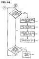
- FIG. 6A a flow chart of the initial steps of the image analysis process is illustrated.
- the process begins with steps 300 to 304 wherein certain information is initially read into the memory 42. In the preferred embodiment, however, this information is obtained from a read-only memory associated with the CPU 38. This memory is merely addressed and the information is thereafter transferred via the multibus 46 to the memory 42.
- Step 300 relates to the accessing and storing of a window correlation table (a cross correlation between lead count and window index value).
- Step 302 relates to the reading of a threshold value for the CIU 50. This defines what analog voltage level from the camera 24 is to be used as the cross-over point between a light and dark image connotation. Higher than the threshold value will be interpreted by the CIU 50 as light or a binary zero.
- Step 304 involves the reading into memory of an "M" mask table.
- This table consists of a number of eight bit masks that are to be successively applied to certain bit strings of information in a manner that will be described in detail hereinafter.
- the central processor 38 awaits a picture authorization communication from the CPU 36 via the bus 48.
- the central processor 38 pursues the "yes" path to a step 310 and reads the width and lead information identifying the component whose leads have been inserted.
- the central processor 38 thereafter stores the lead information as a numerical value in the software variable "lead total" in step 312.
- the central processor also reads the table of X i , Y i coordinate values for the identified component width in a step 314.
- the table of X i , Y i coordinates will be the coordinate values for each window W i .
- the central processor 38 now proceeds to step 316 and exits to an operating mode program.
- the central processor unit 38 merely awaits a keyboard entry from the terminal 60 in a step 318. In the event that a keyboard entry is made, the central processor unit 38 exits to a diagnostic program in a step 320.
- the central processor 38 will return through the re-entry point A and await a picture authorization in step 308. The central processor 38 will then exit to an operating program.
- the operating mode program begins with a step 400 wherein the threshold value (initially stored in the software reference "T" in step 304) is transmitted to the CIU 50.
- Each so characterized pixel voltage is stored as either a binary one (dark) or binary zero (light) in step 402.
- the central processor unit 38 proceeds to a step 404 and awaits the completion of this storage. This will be indicated to the central processor 38 by a status signal from the CIU 50.
- a status signal from the CIU 50.
- These pixel bits will be stored in the CIU memory as addressable bytes in accordance with the addressing scheme previously discussed relative to Figure 5.
- the central processor 38 proceeds to step 406 and sets the window index variable "I", equal to one.
- the central processor 38 then proceeds to step 407 and sets the "lead count” variable equal to one.
- the central processor 38 now proceeds to a step 408 and sets a window row array index "J" equal to one. It is to be noted that this index will always be set equal to one each time the central processor returns to the step 408 via a return point B.
- the central processor 38 proceeds from step 408 to a step 410 and obtains the X i and Y i coordinates for the current value of the window index variable "I".
- step 406 Since this variable is initially set equal to one in step 406, the first pass through step 410 will result in the coordinates X1 and Y1 being obtained. These coordinates will be stored in step 412.
- the central processor 38 now proceeds to a step 414 and calculates a "base address" using the coordinate value of Y i (the first addressable byte in any given Y-row in Figure 5).
- the central processor 38 now proceeds to step 416 and divides the X i coordinate value by eight and saves both the dividend "D" and the remainder "R” of this division operation.
- step 417 a window row array index "K” is set equal to one.
- the Dividend "D" is thereafter added to the "base address” and saved as a "current address” in step 418.
- the central processor 38 now proceeds to step 420 and reads the addressable byte of information from the CIU 50 as defined by the current address. This byte of information is saved as "byte 1".
- the central processor 38 now proceeds to step 422 in Figure 7B and increments the value of the current address by one.
- the addressable byte in the CIU defined by the thus incremented address is stored as "byte 2". It is to be appreciated that the steps 418 through 422 have located two bytes of information in the CIU memory which contain the pixel bits for the bottom-most row of pixels in the first window W1. It, therefore, remains to isolate the particular eight pixel bits from the bytes identified as byte 1 and byte 2.
- step 424 The extraction of meaningful pixel bits from these two bytes begins with step 424 wherein the bits of byte 1 beginning with bit position 7-R are extracted. This effectively disregards any bits in byte 1 that are not a pixel bit within the window.
- Each extracted bit is stored as a particular bit in a window bit array B jk .
- the first bit to be extracted in step 424 will be stored as a bit B11 whereas the second extracted bit will be stored as a bit B12. This will continue until the bit of byte 1 corresponding to bit position zero is stored as a bit in the window bit array. It is to be noted that if "R" equals zero then all eight bits of byte 1 will have been stored as a row of bits in the window bit array.
- the central processor 38 will proceed through step 426 to step 428 and compute a new base address for the next row of bits.
- the central processor 38 will otherwise proceed to a step 430 and extract the bits out of byte 2 beginning with bit position 7 and extending to bit position 8-R.
- the thus extracted bits are stored as the last remaining bits in the particular row of bits of the window bit array currently being formed. In other words, the last bit to be extracted from byte 2 will become bit B18 in the window bit array.
- the central processor 38 will now proceed to step 428 and calculate a new base address for the next row of pixel bits to be examined for particular window bits.
- the central processor 38 will then proceed to step 432 and increment the window array row index "J" by one.
- step 434 This will allow the next extracted bits from bytes 1 and 2 to be stored in row 2 of the window bit array. This occurs when the central processor 38 proceeds through step 434 back through the re-entry point C to step 418 in Figure 7A and again calculates the appropriate addresses for bytes 1 and 2 in steps 420, 422 and thereafter extracts the appropriate window bits in steps 424, 426 and 430.
- the appropriate row of bits within the window bit array B jk is formed upon the reiteration of these steps through to and including the formation of row eight.
- the central processor 38 proceeds through step 434 to step 436.
- the window bit array is rotated so that each previously formed column of window bits becomes a correspondingly numbered row in a rotated window bit array.
- the new rotated column or row index is "L”.
- the "L” index is set equal to eight in step 438 and the eight transposed bits comprising row eight of the rotated window bit array are fetched in step 440.
- the central processor 38 now proceeds to a step 442 wherein the eight transposed bits are successively compared with bit pattern masks illustrated in an "M" mask table of Figure 8.
- each of the bit pattern masks defines a bit pattern having at least six consecutive binary one bits.
- the central processor will proceed to a step 444 in Figure 7D and set a test flag "F i " equal to one indicating that at least one rotated column of window bits from the window bit array B jk has been found to have at least six successive binary one bits. Since the test flag "F i " is itself indexed by the window index "I", the particular test flag will be specific to the window then under examination.
- step 442 in the event that the particular fetched bits of step 440 do not contain six consecutive binary one bits, then the central processor 38 will proceed to a step 446 and decrement the "L" index.
- the process defined by steps 440, 442 and 446 will again be repeated by virtue of step 448.
- the next rotated column of window bits indicated by the new "L” will be fetched and compared with the "M” masks. This reiteration will continue until either a rotated column is found to have six consecutive binary one bits or all eight rotated columns have been examined. In the latter event, the "L" index will have been decremented to zero causing the central processor to proceed through step 448 to step 450 wherein the index "L” is again set equal to eight.
- the central processor now fetches both the rotated column of window bits identified by "L” in a step 452 as well as the next rotated column of window bits identified by "L-1” in a step 454. These two successively fetched rotated columns of eight bits each are now logically ORed together in a step 456.
- the resultant eight bits are now compared in a step 458 with each of the bit pattern masks in the "M" mask table of Figure 8. In the event that the resultant eight bits contain six consecutive binary one bits, then the central processor 38 immediately proceeds out of step 458 to the step 444 in Figure 7d via their re-entry point D. This indicates that at least two successive columns of the window bit array B jk can be combined to show a continuous string of six consecutive binary one bits.
- step 456 if a binary one bit is missing from a bit position in one column of the window bit array B jk but found in the corresponding bit position of the immediately adjacent column, then the logical OR operation of step 456 will have produced a binary one bit in the resultant eight bit string being compared with the "M" masks in Figure 8. This will constitute a "pass” condition being indicated by the test flag "F i " in step 444.
- step 458 in Figure 7E if the resultant eight bits formed in step 456 do not indicate a continuous string of at least six consecutive binary one bits, then the index "L" is decremented in step 460 and the process of steps 452, 454, 456 and 458 is again repeated in a step 462 and re-entry point E. This continues to occur until either six consecutive binary one bits are found in two combined adjacent columns of the window bit array or the index "L" has been decremented to one. In the latter case the central processor 38 proceeds through step 462 to a step 464 and sets the test flag "F i " equal to zero indicating a "fail" condition.
- test flag "F i " is set equal to zero in step 464 or set equal to one in step 444, the central processor 38 will always proceed from either step to a step 466 in Figure 7F.
- the central processor 38 compares the current value of "lead count” to the value of "lead total".
- “lead total” is defined in a step 312 as the number of leads for the component that is being inserted.
- the software variable "lead count” is initially set equal to one in a step 407. Since most components will have several leads, the central processor will proceed to increment "lead count” in a step 468. The incremented "lead count” of step 468 will now be used in a step 470 to define the next window which is to be examined for the presence or absence of a lead.
- the central processor 38 will proceed to the window correlation table and read the value of "I” for the incremented "lead count” of step 468.
- the central processor 38 will now proceed via return point B to Figure 7A and again initialize the window row index "J" equal to one in step 408.
- the central processor will then proceed to go to the table of X i , Y i coordinates and obtain the coordinates for "I". These coordinates will be stored in step 412 and the "base address" for the Y i coordinate will be calculated in step 414.
- the X i coordinate will be divided by eight in step 416 and both the dividend "D" and the remainder "R” will be saved.
- the two bytes within the Y i row will then be identified and the eight window bits within these two bytes will be extracted and set equal to the first row of the newly constructed window bit array B jk .
- the columns will be rotated and examined for six consecutive binary one bits in any one column or in the resultant eight bits formed by combining two adjacent columns by the logical OR operation of step 456.
- the test flag "F i " for the particular window under examination will either be set equal to one in step 444 or set equal to zero in step 464 before returning to step 466 in Figure 8F.
- the central processor 38 will continue through the above steps until such time as the "lead count" equals "lead total” in step 466.
- the central processor 38 will proceed to a step 472 in Figure 8F and again set the software variable "lead count” equal to one.
- the central processor 38 then proceeds to set "I” equal to one in a step 474 and obtains the particular "F i " corresponding to the value of "I” in step 476.
- the value of the thus obtained “F i " is checked for a failure condition in a step 478.
- the central processor 38 will immediately exit to a step 480 and transmit a "fail" signal to central processor 36.
- the central processor will proceed to a step 482 and check as to whether "lead count” equals "lead total”. In the event that the "lead count” remains less than “lead total”, the central processor will proceed to increment the "lead count” in a step 484 and read the current value of "I” for the incremented "lead count” in step 486.
- the "F i " corresponding to the thus incremented value of "I” will be obtained in step 476 and analyzed as to failure in step 478. This will continue to occur until such time as a particular "F i " is equal to zero or until the "lead count” is equal to "lead total”. In the latter event, the central processor 38 will exit from step 482 to a step 488 and send a "pass” message to the central processor 36.
Landscapes
- Engineering & Computer Science (AREA)
- Operations Research (AREA)
- Manufacturing & Machinery (AREA)
- Microelectronics & Electronic Packaging (AREA)
- Image Analysis (AREA)
- Testing Of Short-Circuits, Discontinuities, Leakage, Or Incorrect Line Connections (AREA)
Claims (5)
- System zur Überprüfung der richtigen Einsteckung von Anschlüssen eines elektronischen Bauelementes (10) wie einem DIP in eine Leiterplatte (16) vor dem Festmachen der Anschlüsse an die Platte, wobei das System aufweist:
eine Kameraeinrichtung (24) einschließlich einer Vielzahl von photoempfindlichen Binärelementen, die in horizontalen und vertikalen Reihen angeordnet sind, um eine zweidimensionale Matrix festzulegen, wobei jene Elemente angeordnet sind, um einen Wert auszugeben, wenn der Anschluß vorhanden ist und das Bild des Anschlusses darauffällt, und einen anderen Wert, wenn das Bild dort nicht vorhanden ist, und
eine Einrichtung (34), die angeordnet ist, um zu bestimmen, ob jeder der Bauelementanschlüsse (LC1 - LC 40) vorhanden ist durch Untersuchung einer Menge von diskreten Fenstern (W1-W40) der photoempfindlichen Elemente, wobei ein Fenster mit jedem Anschluß verknüpft ist, wobei jeder Anschluß eine Vielzahl von aufeinanderfolgenden horizontalen Reihen von den Elementen und eine Vielzahl von aufeinanderfolgenden vertikalen Reihen von den Elementen aufweist, wobei die festlegende Einrichtung (34) eine Einrichtung aufweist, die angeordnet ist, um zu ermitteln, ob eine der vertikalen Reihen von photoempfindlichen Elementen innerhalb eines Fensters oder einer Verbindung einer ausgewählten Anzahl der vertikalen Reihen von photoempfindlichen Elementen innerhalb eines Fensters eine vorbestimmte Anzahl von aufeinanderfolgenden Elementen darstellt, die einen Wert aufweisen, der anzeigt, daß ein Anschluß vorhanden ist. - System gemäß Anspruch 1, dadurch gekennzeichnet, daß die Fenster (W1 - W40) etwa acht Reihen breit und etwa acht Reihen hoch sind.
- System gemäß einem der Ansprüche 1 und 2, dadurch gekennzeichnet, daß das Bild eines Anschlusses so angeordnet ist, um eine Fläche von etwa acht Elementen lang und etwa drei Elementen breit auf dem Matrix der photoempfindlichen Elemente einzunehmen.
- System gemäß einem der Ansprüche 1 bis 3 dadurch gekennzeichnet, daß die ausgewählte Anzahl der vertikalen Reihen zwei beträgt.
- System gemäß einem der Ansprüche 1 bis 4, dadurch gekennzeichnet, daß die vorbestimmte Anzahl von aufeinanderfolgenden Elementen etwa sechs beträgt.
Applications Claiming Priority (2)
| Application Number | Priority Date | Filing Date | Title |
|---|---|---|---|
| US07/029,834 US4862510A (en) | 1987-03-24 | 1987-03-24 | Lead sense system for component insertion machine |
| US29834 | 1993-03-11 |
Publications (3)
| Publication Number | Publication Date |
|---|---|
| EP0284381A2 EP0284381A2 (de) | 1988-09-28 |
| EP0284381A3 EP0284381A3 (en) | 1989-11-29 |
| EP0284381B1 true EP0284381B1 (de) | 1993-06-23 |
Family
ID=21851142
Family Applications (1)
| Application Number | Title | Priority Date | Filing Date |
|---|---|---|---|
| EP88302591A Expired - Lifetime EP0284381B1 (de) | 1987-03-24 | 1988-03-24 | System zur Erkennung von Bauelemente-Anschlüssen für eine Bauelemente-Einsteckmaschine |
Country Status (5)
| Country | Link |
|---|---|
| US (1) | US4862510A (de) |
| EP (1) | EP0284381B1 (de) |
| JP (1) | JPS6413470A (de) |
| CA (1) | CA1271265A (de) |
| DE (1) | DE3881924T2 (de) |
Families Citing this family (13)
| Publication number | Priority date | Publication date | Assignee | Title |
|---|---|---|---|---|
| JP2727361B2 (ja) * | 1989-07-22 | 1998-03-11 | 株式会社新川 | マーキング装置における版監視方法及び装置 |
| US5030839A (en) * | 1989-12-13 | 1991-07-09 | North American Philips Corporation | Method and apparatus for measuring body to lead tolerances of very odd components |
| US5124644A (en) * | 1990-12-19 | 1992-06-23 | Vlsi Technology, Inc. | System for positioning a semiconductor chip package with respect to a testing device |
| US5216804A (en) * | 1991-05-21 | 1993-06-08 | U.S. Philips Corp. | Method and device for placing a component on a printed circuit board |
| JPH07115296A (ja) * | 1993-10-15 | 1995-05-02 | Sanyo Electric Co Ltd | 部品実装機の制御装置 |
| US5467408A (en) * | 1994-04-22 | 1995-11-14 | The Gillette Company | Ball point writing quality analysis |
| JP3922310B2 (ja) * | 1995-08-25 | 2007-05-30 | 三菱瓦斯化学株式会社 | アクリル酸またはメタクリル酸のグリシジルエステルの製造方法 |
| KR19980039100A (ko) * | 1996-11-27 | 1998-08-17 | 배순훈 | 부품의 클린칭 방향을 이용한 미삽 검사장치 및 방법 |
| JP3907786B2 (ja) * | 1997-06-16 | 2007-04-18 | 松下電器産業株式会社 | 電子部品実装方法及び装置 |
| US6571006B1 (en) * | 1998-11-30 | 2003-05-27 | Cognex Corporation | Methods and apparatuses for measuring an extent of a group of objects within an image |
| US6824485B2 (en) | 2002-07-09 | 2004-11-30 | The Gates Corporation | Power transmission belt |
| DE102006027662A1 (de) * | 2006-06-14 | 2007-12-20 | Siemens Ag | Verfahren zur Datenübertragung zwischen einer Bestückkopf-Steuereinrichtung und einer zentralen Steuereinrichtung in einem Bestückautomat, Bestückautomat, Bestückkopf, senderseitige Übertragungseinrichtung und System aus senderseitiger und empfängerseitiger Übertragungseinrichtung |
| CN115333735B (zh) * | 2022-10-11 | 2023-03-14 | 浙江御安信息技术有限公司 | 一种数据的安全传输方法 |
Family Cites Families (9)
| Publication number | Priority date | Publication date | Assignee | Title |
|---|---|---|---|---|
| EP0041870B1 (de) * | 1980-06-10 | 1986-12-30 | Fujitsu Limited | Vorrichtung für die Erkennung der Lage eines Motives |
| US4553843A (en) * | 1981-08-03 | 1985-11-19 | Micro Component Technology, Inc. | Apparatus for determining the alignment of leads on a body |
| US4464833A (en) * | 1982-09-01 | 1984-08-14 | Usm Corporation | Variable rate control logic for component insertion machine |
| US4549087A (en) * | 1982-12-27 | 1985-10-22 | Usm Corporation | Lead sensing system |
| JPS60247106A (ja) * | 1984-05-22 | 1985-12-06 | Fujitsu Ltd | 形状検査装置 |
| US4696047A (en) * | 1985-02-28 | 1987-09-22 | Texas Instruments Incorporated | Apparatus for automatically inspecting electrical connecting pins |
| JPS61290311A (ja) * | 1985-06-19 | 1986-12-20 | Hitachi Ltd | はんだ付部の検査装置及びその方法 |
| US4799268A (en) * | 1985-11-12 | 1989-01-17 | Usm Corporation | Lead sense system for component insertion machine |
| JPS62195509A (ja) * | 1986-02-24 | 1987-08-28 | Mitsubishi Electric Corp | 電子部品形状検査装置 |
-
1987
- 1987-03-24 US US07/029,834 patent/US4862510A/en not_active Expired - Fee Related
-
1988
- 1988-03-23 CA CA000562235A patent/CA1271265A/en not_active Expired - Lifetime
- 1988-03-24 DE DE88302591T patent/DE3881924T2/de not_active Expired - Fee Related
- 1988-03-24 EP EP88302591A patent/EP0284381B1/de not_active Expired - Lifetime
- 1988-03-24 JP JP63070857A patent/JPS6413470A/ja active Pending
Also Published As
| Publication number | Publication date |
|---|---|
| CA1271265A (en) | 1990-07-03 |
| JPS6413470A (en) | 1989-01-18 |
| US4862510A (en) | 1989-08-29 |
| DE3881924D1 (de) | 1993-07-29 |
| EP0284381A2 (de) | 1988-09-28 |
| DE3881924T2 (de) | 1993-11-04 |
| EP0284381A3 (en) | 1989-11-29 |
Similar Documents
| Publication | Publication Date | Title |
|---|---|---|
| EP0284381B1 (de) | System zur Erkennung von Bauelemente-Anschlüssen für eine Bauelemente-Einsteckmaschine | |
| EP0240203A2 (de) | Optischer Karten-Abtaster | |
| US4853888A (en) | Programmable multifunction keyboard | |
| US7061533B1 (en) | Image processing apparatus | |
| EP1443452B1 (de) | Zweidimensionaler Kode, Vorrichtung und Verfahren zum Erzeugen, Anzeigen und Lesen desselben | |
| US4799268A (en) | Lead sense system for component insertion machine | |
| EP0372762A2 (de) | Minutiae-Ermittlung für Fingerabdruck-Identifikation | |
| US5430283A (en) | Bar-code symbol reading apparatus | |
| US4527283A (en) | Character information separating apparatus for printed character reading systems | |
| KR20120023646A (ko) | 2차원 심볼 코드 및 이 심볼 코드를 판독하는 방법 | |
| US4218673A (en) | Pattern matching method and such operation system | |
| US4845768A (en) | Method and circuit arrangement for editing slanting characters, particularly handwritten characters | |
| EP0382293B1 (de) | Verfahren und Gerät zur Umwandlung der Auflösung eines Bildes mit Muster aus bivalenten Pixeln | |
| EP0294716A2 (de) | Gerät zum Detektieren von Kammlinienmustern | |
| WO1985000683A1 (en) | Personal identification method and apparatus | |
| US3218439A (en) | Vote tallying machine | |
| US5736723A (en) | Method and apparatus for identifying the orientation of a dot matrix code marking of an article | |
| EP0736835B1 (de) | Verfahren zum Lesen eines Punkt-Matrix-Kodes auf einem Gegenstand | |
| US6839848B1 (en) | Information processing system and peripheral apparatus | |
| US3965335A (en) | Programable data entry system | |
| EP0127249A2 (de) | Musterdatenverarbeitungsanlage | |
| JPH0120795B2 (de) | ||
| JP2819369B2 (ja) | 画像ヘッドの組立方法 | |
| US4135461A (en) | Stitch pattern selection and display arrangement for sewing machines | |
| JPH05159122A (ja) | タイムレコーダ |
Legal Events
| Date | Code | Title | Description |
|---|---|---|---|
| PUAI | Public reference made under article 153(3) epc to a published international application that has entered the european phase |
Free format text: ORIGINAL CODE: 0009012 |
|
| AK | Designated contracting states |
Kind code of ref document: A2 Designated state(s): DE FR GB |
|
| PUAL | Search report despatched |
Free format text: ORIGINAL CODE: 0009013 |
|
| AK | Designated contracting states |
Kind code of ref document: A3 Designated state(s): DE FR GB |
|
| RAP1 | Party data changed (applicant data changed or rights of an application transferred) |
Owner name: EMHART INDUSTRIES, INC. |
|
| 17P | Request for examination filed |
Effective date: 19900425 |
|
| RAP1 | Party data changed (applicant data changed or rights of an application transferred) |
Owner name: DYNAPERT INC. |
|
| RAP1 | Party data changed (applicant data changed or rights of an application transferred) |
Owner name: EMHART INC. |
|
| 17Q | First examination report despatched |
Effective date: 19920831 |
|
| GRAA | (expected) grant |
Free format text: ORIGINAL CODE: 0009210 |
|
| AK | Designated contracting states |
Kind code of ref document: B1 Designated state(s): DE FR GB |
|
| REF | Corresponds to: |
Ref document number: 3881924 Country of ref document: DE Date of ref document: 19930729 |
|
| ET | Fr: translation filed | ||
| PG25 | Lapsed in a contracting state [announced via postgrant information from national office to epo] |
Ref country code: GB Effective date: 19940324 |
|
| PLBE | No opposition filed within time limit |
Free format text: ORIGINAL CODE: 0009261 |
|
| STAA | Information on the status of an ep patent application or granted ep patent |
Free format text: STATUS: NO OPPOSITION FILED WITHIN TIME LIMIT |
|
| 26N | No opposition filed | ||
| GBPC | Gb: european patent ceased through non-payment of renewal fee |
Effective date: 19940324 |
|
| PG25 | Lapsed in a contracting state [announced via postgrant information from national office to epo] |
Ref country code: FR Effective date: 19941130 |
|
| PG25 | Lapsed in a contracting state [announced via postgrant information from national office to epo] |
Ref country code: DE Effective date: 19941201 |
|
| REG | Reference to a national code |
Ref country code: FR Ref legal event code: ST |