EP0283778A1 - Verfahren zur thermischen Charakterisierung des Gehäuses von Halbleiterbaueinheiten - Google Patents
Verfahren zur thermischen Charakterisierung des Gehäuses von Halbleiterbaueinheiten Download PDFInfo
- Publication number
- EP0283778A1 EP0283778A1 EP88103148A EP88103148A EP0283778A1 EP 0283778 A1 EP0283778 A1 EP 0283778A1 EP 88103148 A EP88103148 A EP 88103148A EP 88103148 A EP88103148 A EP 88103148A EP 0283778 A1 EP0283778 A1 EP 0283778A1
- Authority
- EP
- European Patent Office
- Prior art keywords
- resistor
- temperature
- package
- resistance
- reference point
- Prior art date
- Legal status (The legal status is an assumption and is not a legal conclusion. Google has not performed a legal analysis and makes no representation as to the accuracy of the status listed.)
- Withdrawn
Links
- 238000000034 method Methods 0.000 title claims abstract description 49
- 239000004065 semiconductor Substances 0.000 title claims abstract description 47
- 238000004806 packaging method and process Methods 0.000 title claims abstract description 21
- 238000012512 characterization method Methods 0.000 title description 4
- BASFCYQUMIYNBI-UHFFFAOYSA-N platinum Chemical compound [Pt] BASFCYQUMIYNBI-UHFFFAOYSA-N 0.000 claims abstract description 53
- 229910052697 platinum Inorganic materials 0.000 claims abstract description 28
- 238000012360 testing method Methods 0.000 claims abstract description 17
- 239000000758 substrate Substances 0.000 claims description 10
- 229910052710 silicon Inorganic materials 0.000 claims description 4
- 239000010703 silicon Substances 0.000 claims description 4
- PCHJSUWPFVWCPO-UHFFFAOYSA-N gold Chemical compound [Au] PCHJSUWPFVWCPO-UHFFFAOYSA-N 0.000 claims description 3
- 239000010931 gold Substances 0.000 claims description 3
- 229910052737 gold Inorganic materials 0.000 claims description 3
- XUIMIQQOPSSXEZ-UHFFFAOYSA-N Silicon Chemical compound [Si] XUIMIQQOPSSXEZ-UHFFFAOYSA-N 0.000 claims 3
- 230000001419 dependent effect Effects 0.000 description 4
- 230000017525 heat dissipation Effects 0.000 description 4
- 238000005259 measurement Methods 0.000 description 4
- 239000000463 material Substances 0.000 description 3
- 238000004088 simulation Methods 0.000 description 3
- 238000009835 boiling Methods 0.000 description 2
- 239000000919 ceramic Substances 0.000 description 2
- 229910052751 metal Inorganic materials 0.000 description 2
- 239000002184 metal Substances 0.000 description 2
- 230000003287 optical effect Effects 0.000 description 2
- 239000005022 packaging material Substances 0.000 description 2
- XLYOFNOQVPJJNP-UHFFFAOYSA-N water Substances O XLYOFNOQVPJJNP-UHFFFAOYSA-N 0.000 description 2
- 238000009529 body temperature measurement Methods 0.000 description 1
- 238000004364 calculation method Methods 0.000 description 1
- 239000011248 coating agent Substances 0.000 description 1
- 238000000576 coating method Methods 0.000 description 1
- 238000010276 construction Methods 0.000 description 1
- 230000006378 damage Effects 0.000 description 1
- 238000013461 design Methods 0.000 description 1
- 238000005516 engineering process Methods 0.000 description 1
- 238000012423 maintenance Methods 0.000 description 1
- 238000004519 manufacturing process Methods 0.000 description 1
- 238000012986 modification Methods 0.000 description 1
- 230000004048 modification Effects 0.000 description 1
- 238000000611 regression analysis Methods 0.000 description 1
- 235000002020 sage Nutrition 0.000 description 1
- 239000000523 sample Substances 0.000 description 1
- 238000004544 sputter deposition Methods 0.000 description 1
- 238000002076 thermal analysis method Methods 0.000 description 1
- 238000009966 trimming Methods 0.000 description 1
- 238000001771 vacuum deposition Methods 0.000 description 1
Images
Classifications
-
- G—PHYSICS
- G01—MEASURING; TESTING
- G01R—MEASURING ELECTRIC VARIABLES; MEASURING MAGNETIC VARIABLES
- G01R31/00—Arrangements for testing electric properties; Arrangements for locating electric faults; Arrangements for electrical testing characterised by what is being tested not provided for elsewhere
- G01R31/28—Testing of electronic circuits, e.g. by signal tracer
- G01R31/2851—Testing of integrated circuits [IC]
- G01R31/2896—Testing of IC packages; Test features related to IC packages
-
- G—PHYSICS
- G01—MEASURING; TESTING
- G01K—MEASURING TEMPERATURE; MEASURING QUANTITY OF HEAT; THERMALLY-SENSITIVE ELEMENTS NOT OTHERWISE PROVIDED FOR
- G01K7/00—Measuring temperature based on the use of electric or magnetic elements directly sensitive to heat ; Power supply therefor, e.g. using thermoelectric elements
- G01K7/16—Measuring temperature based on the use of electric or magnetic elements directly sensitive to heat ; Power supply therefor, e.g. using thermoelectric elements using resistive elements
- G01K7/18—Measuring temperature based on the use of electric or magnetic elements directly sensitive to heat ; Power supply therefor, e.g. using thermoelectric elements using resistive elements the element being a linear resistance, e.g. platinum resistance thermometer
- G01K7/183—Measuring temperature based on the use of electric or magnetic elements directly sensitive to heat ; Power supply therefor, e.g. using thermoelectric elements using resistive elements the element being a linear resistance, e.g. platinum resistance thermometer characterised by the use of the resistive element
-
- G—PHYSICS
- G01—MEASURING; TESTING
- G01N—INVESTIGATING OR ANALYSING MATERIALS BY DETERMINING THEIR CHEMICAL OR PHYSICAL PROPERTIES
- G01N25/00—Investigating or analyzing materials by the use of thermal means
- G01N25/18—Investigating or analyzing materials by the use of thermal means by investigating thermal conductivity
-
- G—PHYSICS
- G01—MEASURING; TESTING
- G01R—MEASURING ELECTRIC VARIABLES; MEASURING MAGNETIC VARIABLES
- G01R31/00—Arrangements for testing electric properties; Arrangements for locating electric faults; Arrangements for electrical testing characterised by what is being tested not provided for elsewhere
- G01R31/28—Testing of electronic circuits, e.g. by signal tracer
- G01R31/2851—Testing of integrated circuits [IC]
- G01R31/2855—Environmental, reliability or burn-in testing
- G01R31/2872—Environmental, reliability or burn-in testing related to electrical or environmental aspects, e.g. temperature, humidity, vibration, nuclear radiation
- G01R31/2874—Environmental, reliability or burn-in testing related to electrical or environmental aspects, e.g. temperature, humidity, vibration, nuclear radiation related to temperature
Definitions
- the present invention generally relates to a method for the thermal characterization of packaging materials used to contain semiconductor devices, and more particularly to the use of a platinum resistor test unit designed to accomplish such characterization in a fast and efficient manner.
- DIP dual-in-line
- CERDIP ceramic packages
- metal can-type units metal can-type units
- flat pack small geometry units DIP (dual-in-line) packages made of plastic, ceramic packages (CERDIP), hybrid units, metal can-type units, and flat pack small geometry units.
- junction temperature is defined as the temperature at the surface of the device while it is operating. Temperature extremes as small as 10°C above the T j determined to be "critical" for a particular semiconductor device can reduce its operational lifetime by over one half. Junction temperature values over 160°C will almost always result in very early failure of the device.
- IR method infrared microscope system
- the IR method uses an infrared detector coupled with an optical microscope.
- the surface of the device must first be exposed.
- the optical microscope and attached infrared detector the device can be scanned to generate an average temperature profile, or attention can be directed to individual points on the device.
- the package containing the semiconductor device must be partially opened so that the surface of the device can be viewed. This prevents an accurate determination of the heat dissipation from the device in its native, packaged environment since a portion of the package and any heat sinks attached thereto must be removed.
- the semiconductor device being tested must, in most cases, be coated with a special material having a constant emissivity. Such coating can alter the heat dissipation characteristics of the device, making accurate thermal analysis even more difficult.
- Other disadvantages of the IR method include high equipment and maintenance costs, and limited accuracy.
- V be Pulsed Diode/Transistor V be method
- V be base to emitter voltage
- V f forward voltage
- the temperature-dependent characteristics of these devices may be plotted against externally-applied temperatures to yield a graph.
- the devices are then inserted within a selected package in place of the semiconductor for which it was designed, and a test simulation is run. By using data obtained from the simulation in conjunction with the previously-prepared graph, the thermal characteristics of the package can be determined under various operational conditions.
- the present invention represents a substantial departure from the above-described methods in numerous aspects. Primarily, it avoids the use of expensive test equipment, while increasing the speed, accuracy, and ease with which the thermal characteristics of a semiconductor packaging system may be determined.
- a method for characterizing semiconductor packaging systems uses a platinum resistor test unit.
- the resistor includes a layer of platinum deposited on a substrate which is preferably sized to approximate the overall dimensions of the semiconductor device for which the packaging system was designed. Platinum is used because its resistance and temperature coefficient of resistance (TCR) are highly predictable and reproducible over a wide temperature range.
- TCR temperature coefficient of resistance
- the resistance of the packaged resistor is then determined at multiple temperature levels in order to generate a mathematical correlation between temperature and resistance for the resistor.
- This mathematical correlation may take the form of either a temperature versus resistance graph, and/or a mathematical equation corresponding to the graph from which temperature values may be calculated at selected resistances.
- the packaged resistor is connected to a test circuit having a voltage source which causes the resistor to "self heat” because of the power it dissipates. Thereafter, the voltage across the resistor and current through the resistor is determined. Using this information, the resistance of the resistor can be calculated. The temperature at this resistance can then be obtained from the previously-prepared graph and/or mathematical equation. This temperature is the junction or surface temperature (T j ) of the resistor. Using the T j value thus obtained, the temperature gradient from the surface of the resistor to any pre-selected reference point on or near the outside of the package can be calculated.
- the information obtained using the present invention is useful in determining the heat dissipation capabilities of the packaging system being tested, and represents an accurate simulation as to the amount of heat which will be dissipated through the package when the semiconductor device for which it was designed is installed. As a result, the packaging system can be designed to dissipate the maximum amount of heat.
- the present invention represents a fast and efficient method for determining the thermal characteristics of a packaging system for a semiconductor device. Specifically, the invention enables an accurate determination to be made of the thermal gradient from the surface of a device within the package to any reference point on or near the outside of the package. Such information is useful for the reasons previously discussed.
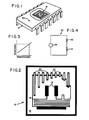
- a semiconductor package is selected for which thermal characterization is desired.
- a DIP (dual-in-line) package 10 is illustrated.
- other packages may be characterized, including ceramic packages (CERDIP), hybrid units, flat pack small geometry packages, and metal can-type packages.
- the platinum resistor 12 is illustrated in Fig. 2, and comprises a substrate 14 (preferably silicon) having a platinum element 16 formed thereon in a serpentine pattern as shown in Fig. 2 to provide maximum resistance while using minimal surface area.
- the platinum element 16 is applied to the substrate 14 using conventional vacuum deposition or sputtering techniques at a thickness of approximately 7,000-10,000 Angstroms. Attached to the platinum element 16 are a plurality of gold terminal pads 18 to which external connection wires (not shown) are attached.
- U.S. Patent 4,186,368 entitled "Wide Range, Quick Response Temperature Probe Sensor.”
- the pattern of the platinum element 16 is designed so that laser trimming or the like may be used to adjust its nominal resistance, if desired.
- a plurality of trimmable elements 20 may be provided as shown in Fig. 2.
- Elements 20 comprise rectangular areas of platinum that may be selectively removed. It is preferred that a 100 ohm (0°C) nominal resistance be used, although other values may be used ranging from 50 to 1,000 ohms, depending on the type of packaging system being tested, and the semiconductor device for which it was designed.
- Platinum was selected for use in the resistor 12 because its resistance and temperature coefficient of resistance (TCR) are highly predictable and reproducible over a wide temperature range.
- TCR temperature coefficient of resistance
- the nominal resistance is a function of the thickness and length of the platinum resistor material, and is traditionally specified at 0°C.
- the 0.0037 and 8.9 ⁇ 10 ⁇ 7 values in the equation represent the TCR of platinum.
- the resistor 12 can be sized to approximate the overall dimensions of the semiconductor device for which the package 10 was designed. This enables a more accurate temperature profile to be obtained in comparison with other methods which make measurements only at single points.
- Thermal calibration involves subjecting the packaged resistor 12 to a first temperature (T1) and measuring the resistance at such temperature.
- T1 a first temperature
- the resistance may be measured by using an ohm meter or other conventional test equipment known to those skilled in the art.
- the packaged resistor 12 is subjected to a second temperature (T2) and the resistance thereof is measured in a similar manner. If desired, measurements at additional temperature levels (T3, T4 ...) can be taken.
- a mathematical correlation between temperature and resistance relative to resistor 12 can now be prepared. For example, a graph of temperature versus resistance can be generated as illustrated in Fig. 3. Because of the above-described characteristics of platinum, the relationship between temperature and resistance is substantially linear as shown. In the alternative, once the resistances are obtained at the specified temperature levels, conventional regression analysis may be used to generate a mathematical equation corresponding to the graph of Fig. 3. The usefulness of this graph and/or mathematical equation will be more fully described below.
- Thermal calibration of the packaged resistor 12 may be accomplished in numerous ways.
- T1 0°C
- T2 100°C
- any procedure may be used which will involve exposure of the resistor 12 to at least two constant and readily determinable temperature values.
- the packaged resistor 12 can now be thermally characterized easily and accurately.
- the resistor 12 is connected to a test circuit having a voltage source.
- the applied voltage across the resistor 12 causes it to "self heat.”
- This may be accomplished using a conventional voltage divider circuit 22 shown in Fig. 4 having a power supply 24 and fixed value resistor 26.
- a voltage divider circuit as used herein, consists of a network of impedance elements connected in series from which one or more voltages can be obtained across any portion of the network.
- resistor 12 is placed in series with fixed value resistor 26.
- the temperature corresponding to the R platinum value determined from the above expression can be obtained from the graph of Fig. 3 or the mathematical equation corresponding thereto. This temperature represents the surface or junction temperature (T j ) of the resistor 12.
- a reference position on the outside of the package 10 is selected.
- a suitable reference position is illustrated in Fig. 1 at 40.
- the temperature at this reference position (T c ) during operation of the resistor is measured. Measurement may be accomplished using a thermocouple or other conventional temperature measurement device.
- reference positions may be selected at a predetermined distance away from the package 10.
- the term "on the outside" of the package 10 as used herein shall be construed to include all exterior reference positions on or away from the package 10.
- T jc temperature gradient from the surface of the resistor 12 to the selected reference position 40
- T j junction temperature of resistor 12
- T c temperature at the selected reference position
- V2 voltage across resistor 12
- I current in the circuit
- T jc temperature gradient from the surface of resistor 12 to the selected reference position in °C/watt
- resistor 12 can be prepared to approximate the size of the semiconductor device for which the package 10 was designed, the information thus obtained is valuable in illustrating how the system will operate and dissipate heat under actual service conditions.
- the package 10 can then be appropriately modified and/or heat sink devices may be secured thereto if necessary.
- a resistor 12 having a nominal resistance of 100 ohms at 0°C was inserted into a package 10, and subsequently calibrated to generate a temperature versus resistance graph similar to that shown in Fig. 3. Calibration occurred at 0°C (T1) and 100°C (T2) using ice and boiling water baths, respectively.
- the resistance of the resistor 12 at 0°C was 100.2 ohms and the resistance of the resistor 12 at 100°C was 138 ohms.
- the voltage divider circuit of Fig. 4 was used.
- the circuit included a 10 volt power supply 24 and 100 ohm fixed resistor 26.
- the resistance value of resistor 12 increased from 100 ohms to 150 ohms due to the power being dissipated in the resistor as it generated heat.
- the temperature of resistor 12 at 150 ohms was then determined to be approximately 135°C using the previously-generated temperature versus resistance graph.
- a reference position on the outside of the package 10 was selected corresponding to that shown at 40 in Fig. 1.
- the temperature at this position was determined to be 90°C.
- T jc for the packaged resistor 12 was then calculated as follows:
Landscapes
- Physics & Mathematics (AREA)
- General Physics & Mathematics (AREA)
- Engineering & Computer Science (AREA)
- Chemical & Material Sciences (AREA)
- Biochemistry (AREA)
- Microelectronics & Electronic Packaging (AREA)
- Health & Medical Sciences (AREA)
- Life Sciences & Earth Sciences (AREA)
- Computer Hardware Design (AREA)
- Analytical Chemistry (AREA)
- General Engineering & Computer Science (AREA)
- General Health & Medical Sciences (AREA)
- Immunology (AREA)
- Pathology (AREA)
- Testing Or Measuring Of Semiconductors Or The Like (AREA)
- Testing Of Individual Semiconductor Devices (AREA)
- Investigating Or Analyzing Materials Using Thermal Means (AREA)
Applications Claiming Priority (2)
| Application Number | Priority Date | Filing Date | Title |
|---|---|---|---|
| US07/023,595 US4734641A (en) | 1987-03-09 | 1987-03-09 | Method for the thermal characterization of semiconductor packaging systems |
| US23595 | 1987-03-09 |
Publications (1)
| Publication Number | Publication Date |
|---|---|
| EP0283778A1 true EP0283778A1 (de) | 1988-09-28 |
Family
ID=21816093
Family Applications (1)
| Application Number | Title | Priority Date | Filing Date |
|---|---|---|---|
| EP88103148A Withdrawn EP0283778A1 (de) | 1987-03-09 | 1988-03-02 | Verfahren zur thermischen Charakterisierung des Gehäuses von Halbleiterbaueinheiten |
Country Status (3)
| Country | Link |
|---|---|
| US (1) | US4734641A (de) |
| EP (1) | EP0283778A1 (de) |
| JP (1) | JPS63243856A (de) |
Cited By (4)
| Publication number | Priority date | Publication date | Assignee | Title |
|---|---|---|---|---|
| EP0523735A1 (de) * | 1991-07-19 | 1993-01-20 | Sumitomo Electric Industries, Limited | Gerät und Verfahren zum Einbrennen |
| US5359285A (en) * | 1991-07-19 | 1994-10-25 | Sumitomo Electric Industries, Ltd. | Method and apparatus for varying temperature and electronic load conditions of a semiconductor device in a burn-in test chamber while performing a burn-in test |
| US5406212A (en) * | 1991-07-19 | 1995-04-11 | Sumitomo Electric Industries, Ltd. | Burn-in apparatus and method for self-heating semiconductor devices having built-in temperature sensors |
| CN102207534A (zh) * | 2011-03-18 | 2011-10-05 | 华南师范大学 | 利用pn结测量LED热阻的方法及其装置 |
Families Citing this family (35)
| Publication number | Priority date | Publication date | Assignee | Title |
|---|---|---|---|---|
| FR2606887B1 (fr) * | 1986-11-18 | 1989-01-13 | Thomson Semiconducteurs | Circuit de mesure des caracteristiques dynamiques d'un boitier pour circuit integre rapide, et procede de mesure de ces caracteristiques dynamiques |
| US4902139A (en) * | 1988-04-13 | 1990-02-20 | General Electric Company | Apparatus and method for measuring the thermal performance of a heated or cooled component |
| US4944035A (en) * | 1988-06-24 | 1990-07-24 | Honeywell Inc. | Measurement of thermal conductivity and specific heat |
| JP3151203B2 (ja) * | 1988-11-23 | 2001-04-03 | テキサス インスツルメンツ インコーポレイテツド | 集積回路の自己検査装置 |
| US5187674A (en) * | 1989-12-28 | 1993-02-16 | Honeywell Inc. | Versatile, overpressure proof, absolute pressure sensor |
| US5177696A (en) * | 1989-12-28 | 1993-01-05 | Honeywell Inc. | Method of determination of gas properties at reference conditions |
| US4994737A (en) * | 1990-03-09 | 1991-02-19 | Cascade Microtech, Inc. | System for facilitating planar probe measurements of high-speed interconnect structures |
| US5263775A (en) * | 1991-02-01 | 1993-11-23 | Aetrium, Inc. | Apparatus for handling devices under varying temperatures |
| CA2073896A1 (en) * | 1991-07-19 | 1993-01-20 | Tatsuya Hashinaga | Burn-in apparatus and method |
| US5302022A (en) * | 1992-12-22 | 1994-04-12 | Vlsi Technology, Inc. | Technique for measuring thermal resistance of semiconductor packages and materials |
| GB9323417D0 (en) * | 1993-11-12 | 1994-01-05 | Univ Waterloo | Non-intrusive state observation of vlsi circuits using thermal actuation |
| BE1008808A3 (nl) * | 1994-10-19 | 1996-08-06 | Imec Inter Uni Micro Electr | Inrichting en werkwijze voor het evalueren van de thermische weerstand van een halfgeleider-component. |
| US5574109A (en) * | 1995-02-01 | 1996-11-12 | Bridgestone Corporation | Aminoalkyllithium compounds containing cyclic amines and polymers therefrom |
| US6046433A (en) * | 1998-09-11 | 2000-04-04 | Linear Technology Corporation | Monolithic integrated circuit die heater and methods for using same |
| US6203191B1 (en) * | 1998-10-28 | 2001-03-20 | Speculative Incorporated | Method of junction temperature determination and control utilizing heat flow |
| US6590405B2 (en) * | 1999-04-21 | 2003-07-08 | Advantest, Corp | CMOS integrated circuit and timing signal generator using same |
| US6433567B1 (en) * | 1999-04-21 | 2002-08-13 | Advantest Corp. | CMOS integrated circuit and timing signal generator using same |
| DE20114544U1 (de) | 2000-12-04 | 2002-02-21 | Cascade Microtech, Inc., Beaverton, Oreg. | Wafersonde |
| US6637930B2 (en) * | 2001-10-02 | 2003-10-28 | International Rectifier Corporation | Method for calculating the temperature rise profile of a power MOSFET |
| WO2003100445A2 (en) | 2002-05-23 | 2003-12-04 | Cascade Microtech, Inc. | Probe for testing a device under test |
| US6984064B1 (en) * | 2002-07-31 | 2006-01-10 | Advanced Micro Devices, Inc. | Thermal transfer measurement of an integrated circuit |
| US6724205B1 (en) | 2002-11-13 | 2004-04-20 | Cascade Microtech, Inc. | Probe for combined signals |
| US7057404B2 (en) | 2003-05-23 | 2006-06-06 | Sharp Laboratories Of America, Inc. | Shielded probe for testing a device under test |
| JP2007517231A (ja) | 2003-12-24 | 2007-06-28 | カスケード マイクロテック インコーポレイテッド | アクティブ・ウェハプローブ |
| KR20070058522A (ko) | 2004-09-13 | 2007-06-08 | 캐스케이드 마이크로테크 인코포레이티드 | 양측 프루빙 구조 |
| US7535247B2 (en) | 2005-01-31 | 2009-05-19 | Cascade Microtech, Inc. | Interface for testing semiconductors |
| US7656172B2 (en) | 2005-01-31 | 2010-02-02 | Cascade Microtech, Inc. | System for testing semiconductors |
| US7327150B2 (en) * | 2005-10-11 | 2008-02-05 | Intel Corporation | Integrated circuit package resistance measurement |
| US7403028B2 (en) | 2006-06-12 | 2008-07-22 | Cascade Microtech, Inc. | Test structure and probe for differential signals |
| US7723999B2 (en) | 2006-06-12 | 2010-05-25 | Cascade Microtech, Inc. | Calibration structures for differential signal probing |
| US7764072B2 (en) | 2006-06-12 | 2010-07-27 | Cascade Microtech, Inc. | Differential signal probing system |
| US7876114B2 (en) | 2007-08-08 | 2011-01-25 | Cascade Microtech, Inc. | Differential waveguide probe |
| JP2011253971A (ja) * | 2010-06-03 | 2011-12-15 | Hitachi Ltd | 電子式制御装置及びその余寿命予測方法 |
| KR101900378B1 (ko) * | 2012-05-25 | 2018-11-02 | 에스케이하이닉스 주식회사 | 리프레쉬회로 |
| CN105004752B (zh) * | 2015-08-12 | 2017-06-27 | 中国电子科技集团公司第四十七研究所 | 多管芯器件热阻测试方法 |
Citations (5)
| Publication number | Priority date | Publication date | Assignee | Title |
|---|---|---|---|---|
| US3982218A (en) * | 1974-09-19 | 1976-09-21 | Corning Glass Works | Temperature sensing device and method |
| EP0105003A1 (de) * | 1982-09-28 | 1984-04-04 | Fujitsu Limited | Verfahren zum Prüfen von kunstharzgekapselten Halbleiterbauelementen |
| WO1986001027A1 (en) * | 1984-07-31 | 1986-02-13 | Rosemount, Inc. | Method for forming a platinum resistance thermometer |
| GB2171252A (en) * | 1985-02-06 | 1986-08-20 | Sharp Kk | A platinum resistor for the measurement of temperature |
| DE3603757A1 (de) * | 1985-02-16 | 1986-08-21 | Nippon Soken, Inc., Nishio, Aichi | Schichtwiderstand fuer eine stroemungsmessvorrichtung |
Family Cites Families (4)
| Publication number | Priority date | Publication date | Assignee | Title |
|---|---|---|---|---|
| US4186368A (en) * | 1978-05-30 | 1980-01-29 | Tektronix, Inc. | Wide range, quick response temperature probe sensor |
| JPS56161649A (en) * | 1980-05-16 | 1981-12-12 | Fujitsu Ltd | Measuring method of thermal resistance of semiconductor package |
| US4695578A (en) * | 1984-01-25 | 1987-09-22 | Glaxo Group Limited | 1,2,3,9-tetrahydro-3-imidazol-1-ylmethyl-4H-carbazol-4-ones, composition containing them, and method of using them to treat neuronal 5HT function disturbances |
| US4684884A (en) * | 1985-07-02 | 1987-08-04 | Gte Communication Systems Corporation | Universal test circuit for integrated circuit packages |
-
1987
- 1987-03-09 US US07/023,595 patent/US4734641A/en not_active Expired - Fee Related
-
1988
- 1988-03-02 EP EP88103148A patent/EP0283778A1/de not_active Withdrawn
- 1988-03-08 JP JP63054725A patent/JPS63243856A/ja active Granted
Patent Citations (5)
| Publication number | Priority date | Publication date | Assignee | Title |
|---|---|---|---|---|
| US3982218A (en) * | 1974-09-19 | 1976-09-21 | Corning Glass Works | Temperature sensing device and method |
| EP0105003A1 (de) * | 1982-09-28 | 1984-04-04 | Fujitsu Limited | Verfahren zum Prüfen von kunstharzgekapselten Halbleiterbauelementen |
| WO1986001027A1 (en) * | 1984-07-31 | 1986-02-13 | Rosemount, Inc. | Method for forming a platinum resistance thermometer |
| GB2171252A (en) * | 1985-02-06 | 1986-08-20 | Sharp Kk | A platinum resistor for the measurement of temperature |
| DE3603757A1 (de) * | 1985-02-16 | 1986-08-21 | Nippon Soken, Inc., Nishio, Aichi | Schichtwiderstand fuer eine stroemungsmessvorrichtung |
Non-Patent Citations (4)
| Title |
|---|
| CONTROL AND INSTRUMENTATION, vol. 18, no. 6, June 1986, pages 114,116,119, London, GB; "Platinum resistance thermometers on film" * |
| IBM TECHNICAL DISCLOSURE BULLETIN, vol. 18, no. 7, December 1975, pages 2383-2384, New York, US; J.E. BAGLIN et al.: "Substrate heating technique for producing local, controlled, uniform high temperature, using low-power density" * |
| JOURNAL OF PHYSICS E; SCIENTIFIC INSTRUMENTS, vol. 7, no. 7, July 1974, pages 543-54, GB; J.W. HILL et al.: "A two-zone resistor with constant-current property" * |
| SOLID STATE TECHNOLOGY, vol. 27, no. 2, February 1984, pages 169-179, Port Washington, New York, US; F.F. OETTINGER: "Thermal evaluation of VLSI packages using test chips - a critical review" * |
Cited By (6)
| Publication number | Priority date | Publication date | Assignee | Title |
|---|---|---|---|---|
| EP0523735A1 (de) * | 1991-07-19 | 1993-01-20 | Sumitomo Electric Industries, Limited | Gerät und Verfahren zum Einbrennen |
| US5327075A (en) * | 1991-07-19 | 1994-07-05 | Sumitomo Electric Industries, Ltd. | Burn-in apparatus and method for semiconductor devices |
| US5359285A (en) * | 1991-07-19 | 1994-10-25 | Sumitomo Electric Industries, Ltd. | Method and apparatus for varying temperature and electronic load conditions of a semiconductor device in a burn-in test chamber while performing a burn-in test |
| US5406212A (en) * | 1991-07-19 | 1995-04-11 | Sumitomo Electric Industries, Ltd. | Burn-in apparatus and method for self-heating semiconductor devices having built-in temperature sensors |
| US5414370A (en) * | 1991-07-19 | 1995-05-09 | Sumitomo Electric Industries, Ltd. | Burn-in apparatus and method which individually controls the temperature of a plurality of semiconductor devices |
| CN102207534A (zh) * | 2011-03-18 | 2011-10-05 | 华南师范大学 | 利用pn结测量LED热阻的方法及其装置 |
Also Published As
| Publication number | Publication date |
|---|---|
| US4734641A (en) | 1988-03-29 |
| JPH0531102B2 (de) | 1993-05-11 |
| JPS63243856A (ja) | 1988-10-11 |
Similar Documents
| Publication | Publication Date | Title |
|---|---|---|
| US4734641A (en) | Method for the thermal characterization of semiconductor packaging systems | |
| JP3872120B2 (ja) | 包装半導体素子の熱インピーダンス評価方法及び装置 | |
| US5842788A (en) | Differential scanning calorimeter | |
| US5997174A (en) | Method for determining a thermal parameter of a device by measuring thermal resistance of a substrate carrying the device | |
| US6508585B2 (en) | Differential scanning calorimeter | |
| US5713666A (en) | Thermal testing apparatus and method | |
| US6796172B2 (en) | Flow sensor | |
| Keltner | Heat flux measurements: theory and applications | |
| Siegal | Practical considerations in high power LED junction temperature measurements | |
| GB2375431A (en) | Device with integrated semiconductor temperature sensor and/or localised heater | |
| Salem et al. | Validation of infrared camera thermal measurements on high-voltage power electronic components | |
| US5852238A (en) | Measuring device and measuring method | |
| US5554938A (en) | Method of evaluating current-driven conductive material | |
| US3828606A (en) | Method for determining thermal fatigue of electronic components | |
| US6186661B1 (en) | Schmidt-Boelter gage | |
| Cian | DeveloDment and Analvsis of an Automated Test System for the Thermal Characterization of IC Packaging Technologies | |
| Berlicki et al. | Thermal thin-film sensors for rms value measurements | |
| JP3284731B2 (ja) | 配線評価装置およびその使用方法 | |
| Górecki et al. | Influence of thermometric characteristics on accuracy of junction temperature measurements of laboratory made SiC Schottky diodes | |
| Bravman et al. | Thermal effects of the operation of high average power Gunn devices | |
| Sofia | Component thermal characterization: transient to steady state | |
| Solbrekken et al. | Calibration of resistance type die level temperature sensors using a single temperature technique | |
| Mindock et al. | Thermal Resistances of Joint Army Navy (JAN) Certified Microcircuit Packages | |
| Adams Jr et al. | Data Reduction Methodology for Fast-Response Schmidt-Boelter Heat-Transfer Gages | |
| Steiger et al. | Practicability of absorption measurements according to ISO/DIS 11551 |
Legal Events
| Date | Code | Title | Description |
|---|---|---|---|
| PUAI | Public reference made under article 153(3) epc to a published international application that has entered the european phase |
Free format text: ORIGINAL CODE: 0009012 |
|
| AK | Designated contracting states |
Kind code of ref document: A1 Designated state(s): DE FR GB |
|
| STAA | Information on the status of an ep patent application or granted ep patent |
Free format text: STATUS: THE APPLICATION IS DEEMED TO BE WITHDRAWN |
|
| 18D | Application deemed to be withdrawn |
Effective date: 19890329 |