EP0280320A2 - Graphics display controller equipped with boundary searching circuit - Google Patents
Graphics display controller equipped with boundary searching circuit Download PDFInfo
- Publication number
- EP0280320A2 EP0280320A2 EP88102895A EP88102895A EP0280320A2 EP 0280320 A2 EP0280320 A2 EP 0280320A2 EP 88102895 A EP88102895 A EP 88102895A EP 88102895 A EP88102895 A EP 88102895A EP 0280320 A2 EP0280320 A2 EP 0280320A2
- Authority
- EP
- European Patent Office
- Prior art keywords
- data
- mask
- bit
- information
- bits
- Prior art date
- Legal status (The legal status is an assumption and is not a legal conclusion. Google has not performed a legal analysis and makes no representation as to the accuracy of the status listed.)
- Granted
Links
Images


Classifications
-
- G—PHYSICS
- G06—COMPUTING; CALCULATING OR COUNTING
- G06T—IMAGE DATA PROCESSING OR GENERATION, IN GENERAL
- G06T11/00—2D [Two Dimensional] image generation
- G06T11/40—Filling a planar surface by adding surface attributes, e.g. colour or texture
-
- G—PHYSICS
- G06—COMPUTING; CALCULATING OR COUNTING
- G06T—IMAGE DATA PROCESSING OR GENERATION, IN GENERAL
- G06T7/00—Image analysis
- G06T7/10—Segmentation; Edge detection
- G06T7/12—Edge-based segmentation
Definitions
- the present invention relates to a graphics display controller which controls a display memory to display figures on a display screen of a raster scan cathode-ray tube, and more particularly to a boundary searching circuit provided in such a controller to determine a boundary of an area to be painted.
- One of various functions performed by a graphics display controller is to paint or fill a closed area with a certain color or with an arbitrary pattern. To this end, it is required to search or determine a boundary of the area to be painted. Since each picture element on a display screen corresponds to each bit in a display memory, the boundary of the painting area is searched by detecting the data of the display memory.
- the boundary searching is executed in general in accordance with the following procedure:
- the left-hand boundary searching and the right-hand boundary searching are performed with respect to other words arranged in other horizontal lines on the display screen.
- the boundary of the area to be painted is searched.
- the data of each word is detected one bit by one bit by use of a bit-shift instruction. For this reason, a very long processing time is required. For example, in case where 1000 bits are present between the left-hand boundary and the right-hand boundary, the bit-shift instruction and the data detecting operation are executed 1000 times.
- an object of the present invention is to provide a graphics display controller equipped with a boundary searching circuit which searches the boundary of an area to be painted at a high speed.
- Another object of the present invention is to provide a boundary searching circuit in which the boundary of an area to be painted is detected without using a bit-shift instruction.
- a graphics display controller comprises means responsive to control data for generating mask information consisting of N bits (N being an integer more than 1) in which M bits has mask data (M being zero to N-1), means for reading display data consisting of N bits from a display memory, means supplied with the mask information and the display data for outputting data of the bit or bits of the display data corresponding to the bit or bits of the mask information which do not have the mask data, means responsive to the outputted data for generating bit position information relative to a position of the bit having data of a predetermined logic level.
- the control data designates the number of bits having the mask data and/or the position thereof in the mask information.
- first mask information is generated in which all bits except for the bit of a position corresponding to the position of the searching start bit take the mask data. Accordingly, only the data of the searching start bit is supplied to the bit position information generating means. If the data of the searching start bit is the predetermined logic level, "1" for example, the information is generated which represents that the boundary searching operation is to be terminated. On the other hand, in case where the data of the searching start bit is "0", a left-direction boundary searching operation starts. Second mask information is thus generated in which at least the right-end bit to the associated bit with the searching start bit take the mask data.
- the data from the left-end bit to the bit adjacent leftward to the searching start bit in the first word are supplied to the bit position information generating means, and if the data "1" is present among them, the position information relative to the bit stored with the data "1" is obtained.
- a second word adjacent leftward to the first word is read from the display memory, and third mask information is generated in which all the bits do not mask data.
- the data of all bits of the second word are supplied to the bit position information generating means. If the second word includes a bit stored with the data "1", the position information relative to the position of that bit is obtained. In case where the bit of data "1" is not present in the second word, a third word adjacent leftward to the second word is read out. No bit of the mask information takes the mask data.
- a right-hand boundary searching operation is executed similarly. Thus, the boundary of the area to be painted is searched for a short time.
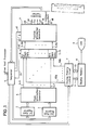
- a graphics display controller includes a sequencer 1 and a display memory control circuit 7, for controlling a display memory 8 to display figures and/or characters on a display screen of a raster scan type cathode-ray tube (CRT) 9.
- Each bit in the display memory 8 represents each picture element on the screen of the CRT 9.
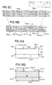
- Sixteen bits constitute one word in the memory 8. It is assumed that the memory 8 stores a figure 100 as shown in Fig. 10A, which is displayed on the screen of CRT 9, and the sequencer 1 receives an instruction from a host processor (not shown) to "paint", or fill, the closed area of the figure 100 with a certain color or with a number of small patterns.
- a boundary of the painting area 101 as shown in Fig. 10D should be determined. It is defined by such addresses that are one-bit inside the addresses of the boundary of the figure 100 to be painted and it is determined by use of a boundary searching circuit according to the present invention, which includes first and second mask registers 2 and 3, a mask information generator 4, first to sixteenth mask gates 5-0 to 5-15 and a position information generator 6.
- the sequence 1 further receives information representative of a search-starting bit from the host processor. Then, the sequence 1 instructs the display memory controller 7 to read a word including the search-starting bit from the display memory 8. The display memory controller 7 thereby outputs to an address bus 71 address information for accessing the word including the search-start bit and reads the data of the word from the display memory 8 via a data bus 72.
- the sixteen bits data MD0 to MD F of the read-out word are supplied to the first to sixteenth mask gates 5-0 to 5-15, respectively.
- the sequencer 1 further writes control data representative of a position of the search-start bit into both of the first and second mask registers 2 and 3. Since one word of the display memory 8 consists of sixteen bits, the control data written into the mask registers 2 and 3 consists of four bits. The contents of the registers 2 and 3 are supplied to the mask information generator 4.
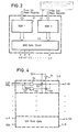
- the mask information generator 4 includes first and second ROMs (read only memories) 41 and 42 and an AND gate circuit 43 consisting of sixteen AND gates (not shown).
- the content of the first mask register 2 is supplied to the first ROM 41 as first address information thereto, and the content of the second mask register 3 is supplied to the second ROM 4 as second address information thereto.
- Each of the first and second address information takes one of sixteen address data "0" to "F”.
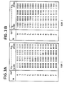
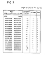
- the first ROM 41 generates sixteen output patterns in response to the address data "0" to "F", respectively, as shown in Fig. 3A.
- the second ROM 42 generates sixteen output patterns in response to the address data "0" to "F", respectively, as shown in Fig. 3B.
- Each of the output patterns generated from the ROMs 41 and 42 consists of sixteen bits X0 to X15 and Y0 to Y15.
- the outputs X0 to X15 from the first mask ROM 41 are supplied to first input terminals of the sixteen AND gates in the circuit 43, respectively, and the outputs Y0 to Y15 from the second mask ROM 42 are supplied to second input terminals of the AND gates, respectively.
- the AND gate circuit 43 generates mask information consisting of sixteen bits 4-0 to 4-F. Assuming that the position data of the search-start bit is "A”, the output of first ROM 41 is "0000 0000 0011 1111" and that of the second ROM 42 is "1111 1111 1110 0000".
- the data of the least significant bit 4-0 through the most significant bit 4-F of the mask information are "0000 0000 0010 0000", as apparent from Figs. 3A and 3B. That is, all the bits 4-0 to 4-9 and 4-B to 4-F except the 11th bit 4-A take mask data "0" and only the 11th bit 4-A takes non-mask data "1".
- the bit data 4-0 to 4-F of the mask information are supplied to the mask gates 5-0 to 5-15, respectively.
- each of the mask gates 5-0 to 5-15 includes an AND gate 54, an inverter 51, two transfer gates 52 and 53 and an OR gate 57 which are connected as shown.
- the transfer gates 52 and 53 are controlled by a logic control signal 55 supplied from the sequencer 1.
- the transfer gate 52 receives the control signal 55 as it is and the gate 53 receives the inverted signal of the control signal 55 by an inverter 56. Therefore, when the logic control signal 55 takes logic "1", the transfer gate 52 is opened and the gate 53 is closed. When the signal 55 takes logic "0”, the gate 52 is closed and the gate 53 is opened. In the data detecting operation of the searching start bit, the logic control signal 55 takes logic "1".
- the position information generator 6 receives searching-direction contol (designation) data 61 and 62 and generates at a set of first output terminals 63 to 66 boundary position information represents which bit among the mask gate outputs 5-00 to 5-150 takes “1" or "0".
- the generator 6 further generates forward information at a second output terminal 67 and back information at a third output terminal 68.
- the forward information represents that the boundary is present in a word which will be thereafter processed, and the back information represents that the boundary is present in a word which was processed just therebefore.
- These boundary position information 63 - 66, forward information 67 and back information 68 are supplied to the sequencer 1.
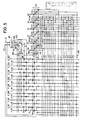
- the position information generator 6 is constructed as shown in Fig. 5 by means of a PLA (programmable logic array) technique.
- each of circular marks disposed at intersections of row signal lines and column signal lines represents an electrical connection therebetween.
- Each of two NAND gates NA, each of two NOR gates NO, each of eighteen AND gates AN1 and each of fifteen OR gates OR respectively execute a NAND operation, a NOR operation, an AND operation and an OR operation with respect to a plurality of inputs denoted by the circular marks.
- Each of transfer gates TG is controlled by the searching-direction control data 61 and 62, a two-to-four decoder 69 and four AND gates AN2.
- Fig. 6 is derived between the input data 5-00 to 5-150 from the mask gates 5-0 to 5-15 and the output data including the boundary position information 63-66, forward information 67 and back information 68.
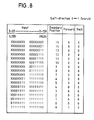
- a second relationship shown in Fig. 7 is derived.
- a third relationship shown in Fig. 8 is obtained in repsonse to the control data 61 and 62 of "10”
- a fourth relationship shown in Fig. 9 is obtained in response to the control data 61 and 62 of "11". More specifically, in Fig.
- the sequencer 1 supplies the searching-direction control data 61 and 62 of "00" to the position information generator 6. Accordingly, the generator 6 generates the information 63-68 in accordance with the relationship shown in Fig. 6. Assuming that the position of the searching start bit is "A" and the data thereof is logic “1”, only the 11th mask gate output 5-100 takes logic "1". Therefore, the content of the boundary position information takes "11". At this time, the forward information 67 and the back information 68 are both logic "0". These information are supplied to the sequencer 1 which thereby regards the searching start bit as locating on the boundary of the area to be painted and terminates the boundary searching operation.
- the sequencer 1 requires a new searching start bit to the host processor.
- the address (a, b) of the search-start bit S is given inside the area 101 as shown in Fig. 10A
- the data of the searching start bit S is logic "0".
- the content of the boundary position information 63-66 is "0" and the forward information 67 of logic "1" is derived.
- the sequencer 1 starts to search a changing point of bit data from the logic "0" to the logic "1" in the left direction of the searching start bit S.
- This search is called hereinafter "left-direction 1 ⁇ 0 search".
- the sequencer 1 generates the logic control signal 55 of logic "1" and the search-direction control data 61 and 62 of "00".
- the left-direction 1 ⁇ 0 search is executed in accordance with the following procedure:
- the sequence 1 thereafter executes a searching operation for detecting a changing point of bit data from logic "0" to logic "1" in the right direction of the searching start bit S.
- This searching operation is called hereinafter "right-direction 0 ⁇ 1 search".
- the logic control signal 55 is maintained to logic "1” and the search-direction control data 61 and 62 are changed to "01". Therefore, the input and output data relationship of the generator 6 is represented by Fig. 7.
- the procedure of the right-direction 0 ⁇ 1 search is as follows:
- the left-hand boundary address (a, i+1) and the right-hand boundary address (a,l-1) are searched in the one horizontal line L a of the painting area 101.
- the boundary searching operation is executed with respect to other lines including lines L a+1 and L a-1 which locate above and under the line L a , respectively, in the same manner as described above. More specifically, a word W a+1,c (or a word W a-1,c ) is read from the display memory 8 and the left-direction 1 ⁇ 0 search is executed with respect to bits and words arranged in the left direction of the bit of the read-out word W a+1,c (or W a-1,c ) having the same column address as the searching start bit S. When this search is completed, the right-direction 0 ⁇ 1 search is executed.
- the painting area 101 has a concave shape. That is, as the data map in a horizontal line L b of the area 101 is shown in Fig. 10C, all the bits defining one portion 100-1 of the closed line figure 100 take logic "1", so that four boundary addresses (b, i+1), (b, j-1), (b, k+1) and (b,l-1) are present in the line L b . For this reason, if these boundary addresses are intended to be detected only by the left-direction 1 ⁇ 0 search and the right-direction 0 ⁇ 1 search, the boundary searching operation is required to be executed twice with respect to each of words in the line L b .
- the boundary searching circuit shown in Fig. 1 can execute a left-direction 0 ⁇ 1 search for searching a changing point of bit data from logic "1" to logic “0" in a left direction of a bit arrangement and a right-direction 1 ⁇ 0 search for searching a changing point of bit data from logic "1" to logic "0” in a right direction of a bit arrangement.
- the logic control signal 55 is changed to "0" level, so that the transfer gates 52 and 53 (see Fig. 4) are turned OFF and ON, respectively. Therefore; each of the mask gates 5-0 to 5-15 holds its outputs to logic "1" when the associated mask information bit takes the mask data "0".
- the search-direction control data 61 and 62 are set to "10", so that the generator 6 takes the input and output data relationship shown in Fig. 8.
- the control data 61 and 62 of "11" are supplied to obtain the relationship shown in Fig. 9.
- the left-direction 0 ⁇ 1 search is executed by masking the data from the MSB to a bit of the same column address as the searching start bit S. Assuming that the column address of the searching start bit S is "A”, the first and second mask registers 2 and 3 are written with the data "0" and “9", respectively. Since all the bits of the read word take logic "1", the generator 6 generates the boundary position information 63-66 of "0" and the forward information 67 of logic "1". The left-direction 0 ⁇ 1 search is thereby executed with respect to each of words arranged in the left direction.
- the mask registers 2 and 3 are written with the data "0" and "F” in order that each of the mask information bits 4-0 to 4-F takes the non-mask data "1".
- the mask gate When a word W b,d including boundary information representative of the second boundary address (b, j-1) is read, the mask gate outputs 5-00 to 5-150 become "0000 0000 0000 0111". Therefore, the content of the boundary position information 63-66 becomes "12" and the forward and back information 67 and 68 take both logic "0", as shown in Fig. 8.
- the sequencer 1 recognizes that the twelfth bit of the word W b,d is the second boundary address (b, j-1).
- the sequencer 1 executes the left-direction 1 ⁇ 0 search with respect to each words arranged in the left direction of the word W b,d to detect the first boundary address (b, i+1).
- the sequencer 1 After the first and second boundary addresses (b, i+1) and (b, j-1) are detected, the sequencer 1 reads again the word arranged in the same column as the word W a,c and then executes the right-direction 1 ⁇ 0 search by masking data from the LSB to the ninth bit.
- the mask registers 2 and 3 are therefore stored with the data "A” and "F", respectively. Since all the bit data of the read word are logic "1", the information 63-66 of "0" and the forward information 67 of "1" are derived.
- the right-direction 1 ⁇ 0 search is repeated with respect to each of words arranged in the right direction.
- the registers 2 and 3 are stored with the data "0" and "F” to obtain the non-mask data "1" from all the mask information bits 4-0 to 4-F.
- the mask gate outputs 5-00 to 5-150 become “1110 0000 0000 0000”.
- the content of the boundary position information 63-66 takes “4" and both of the forward and back information 67 and 68 take logic "0". That is, the sequencer 1 recognizes that the fourth bit of the word W b,e is the third boundary address (b, k+1).
- the boundary searching circuit requires no bit-shift instruction and outputs immediately information representing whether or not the read-out word includes a boundary of an area to be painted.
- the present invention is not limited to the above embodiments, but can be modified and changed without departing from the scope and spirit of the present invention.
- the mask information generator 4 and the position information generator 6 can be constructed by the combination of various gates.
- an area to be painted is defined by a closed line consisting of a string of bit data "0" and all bit data inside the area are logic "1”
- the boundary thereof is detected by employing mainly the left-direction 0 ⁇ 1 search and the right-direction 1 ⁇ 0 search.
- the data of two or more words may be detected simultaneously.
Abstract
Description
- The present invention relates to a graphics display controller which controls a display memory to display figures on a display screen of a raster scan cathode-ray tube, and more particularly to a boundary searching circuit provided in such a controller to determine a boundary of an area to be painted.
- One of various functions performed by a graphics display controller is to paint or fill a closed area with a certain color or with an arbitrary pattern. To this end, it is required to search or determine a boundary of the area to be painted. Since each picture element on a display screen corresponds to each bit in a display memory, the boundary of the painting area is searched by detecting the data of the display memory. The boundary searching is executed in general in accordance with the following procedure:
- (1) A searching start bit is given at random and the data of this searching start bit is detected. If data "1", for example, is stored in the searching start bit, this bit is regarded as being outside the area to be painted and the boundary searching is terminated. A new searching start bit is thus given.
- (2) On the other hand, in case where the data stored at the searching start bit is data "0", detection is made to search whether or not a bit storing data "1" is present between the searching start bit and a left-end bit of a first word including the searching start bit. If the presence of such a bit is detected, a left-hand boundary of the area to be painted is determined.
- (3) In case where the presence of such a bit is not detected, a second word adjacent leftward to the first word is read out and detection is made to search whether or not this second word includes a bit storing data "1". If the second word does not includes such a bit, a third word adjacent leftward to the second word is read out and the data of each bit of the third word is detected. The same processing operation is repeated until an bit storing data "1" is detected. Thus, the left-hand boundary of the area to be painted is searched.
- (4) Next, the searching of a right-end boundary of the area is carried out, by detecting whether or not a bit storing data "1" is present between the searching start bit and a right-end bit of the first word. If the presence of such a bit is not detected, a fourth word adjacent rightward to the first word is read out and the data thereof is judged to detect whether or not the fourth word includes a bit stored with data "1". The same processing operation is executed until a bit stored with data "1" is detected. Thus, a right-hand boundary of the area to be painted is searched.
- Since the above-mentioned first to fourth words are arranged in one horizontal line on the display screen, the left-hand boundary searching and the right-hand boundary searching are performed with respect to other words arranged in other horizontal lines on the display screen. Thus, the boundary of the area to be painted is searched.
- According to prior art, the data of each word is detected one bit by one bit by use of a bit-shift instruction. For this reason, a very long processing time is required. For example, in case where 1000 bits are present between the left-hand boundary and the right-hand boundary, the bit-shift instruction and the data detecting operation are executed 1000 times.
- Therefore, an object of the present invention is to provide a graphics display controller equipped with a boundary searching circuit which searches the boundary of an area to be painted at a high speed.
- Another object of the present invention is to provide a boundary searching circuit in which the boundary of an area to be painted is detected without using a bit-shift instruction.
- A graphics display controller according to the present invention comprises means responsive to control data for generating mask information consisting of N bits (N being an integer more than 1) in which M bits has mask data (M being zero to N-1), means for reading display data consisting of N bits from a display memory, means supplied with the mask information and the display data for outputting data of the bit or bits of the display data corresponding to the bit or bits of the mask information which do not have the mask data, means responsive to the outputted data for generating bit position information relative to a position of the bit having data of a predetermined logic level.
- The control data designates the number of bits having the mask data and/or the position thereof in the mask information. In a processing operation of a first word including a searching start bit, first mask information is generated in which all bits except for the bit of a position corresponding to the position of the searching start bit take the mask data. Accordingly, only the data of the searching start bit is supplied to the bit position information generating means. If the data of the searching start bit is the predetermined logic level, "1" for example, the information is generated which represents that the boundary searching operation is to be terminated. On the other hand, in case where the data of the searching start bit is "0", a left-direction boundary searching operation starts. Second mask information is thus generated in which at least the right-end bit to the associated bit with the searching start bit take the mask data. Therefore, the data from the left-end bit to the bit adjacent leftward to the searching start bit in the first word are supplied to the bit position information generating means, and if the data "1" is present among them, the position information relative to the bit stored with the data "1" is obtained. When the data "1' is not present, a second word adjacent leftward to the first word is read from the display memory, and third mask information is generated in which all the bits do not mask data. The data of all bits of the second word are supplied to the bit position information generating means. If the second word includes a bit stored with the data "1", the position information relative to the position of that bit is obtained. In case where the bit of data "1" is not present in the second word, a third word adjacent leftward to the second word is read out. No bit of the mask information takes the mask data. When a left-hand boundary is detected, a right-hand boundary searching operation is executed similarly. Thus, the boundary of the area to be painted is searched for a short time.
- The above and other objects, advantages and features of the present invention will be more apparent from the following description taken in conjunction with the accompanying drawings, in which
- Fig. 1 is a block diagram representative of an embodiment of the present invention;
- Fig. 2 is a block diagram of a mask information generator shown in Fig. 1;
- Figs. 3A and 3B are table diagrams representative of input and output data relationships of mask ROM's shown in Fig. 2, respectively;
- Fig. 4 is a circuit diagram of each of mask gates shown in Fig. 1;
- Fig. 5 is a circuit diagram of a position information generator shown in Fig. 1;
- Fig. 6, Fig. 7, Fig. 8 and Fig. 9 are table diagrams representative of input and output data relationships of the position information generator shown in Fig. 1, respectively; and
- Figs. 10A, 10B, 10C and 10D are a pattern diagram showing an example of a figure, a data map in a line La of a painting area, a data map in a line Lb of the painting area and a plan view of the painting area, respectively.
- Referring to Fig. 1, a graphics display controller according to an embodiment of the present invention includes a
sequencer 1 and a displaymemory control circuit 7, for controlling adisplay memory 8 to display figures and/or characters on a display screen of a raster scan type cathode-ray tube (CRT) 9. Each bit in thedisplay memory 8 represents each picture element on the screen of theCRT 9. Sixteen bits constitute one word in thememory 8. It is assumed that thememory 8 stores a figure 100 as shown in Fig. 10A, which is displayed on the screen ofCRT 9, and thesequencer 1 receives an instruction from a host processor (not shown) to "paint", or fill, the closed area of the figure 100 with a certain color or with a number of small patterns. At first, a boundary of thepainting area 101 as shown in Fig. 10D should be determined. It is defined by such addresses that are one-bit inside the addresses of the boundary of the figure 100 to be painted and it is determined by use of a boundary searching circuit according to the present invention, which includes first andsecond mask registers mask information generator 4, first to sixteenth mask gates 5-0 to 5-15 and aposition information generator 6. - Turning back to Fig. 1, the
sequence 1 further receives information representative of a search-starting bit from the host processor. Then, thesequence 1 instructs thedisplay memory controller 7 to read a word including the search-starting bit from thedisplay memory 8. Thedisplay memory controller 7 thereby outputs to anaddress bus 71 address information for accessing the word including the search-start bit and reads the data of the word from thedisplay memory 8 via a data bus 72. The sixteen bits data MD₀ to MDF of the read-out word are supplied to the first to sixteenth mask gates 5-0 to 5-15, respectively. Thesequencer 1 further writes control data representative of a position of the search-start bit into both of the first and second mask registers 2 and 3. Since one word of thedisplay memory 8 consists of sixteen bits, the control data written into the mask registers 2 and 3 consists of four bits. The contents of theregisters mask information generator 4. - Referring to Fig. 2, the
mask information generator 4 includes first and second ROMs (read only memories) 41 and 42 and an ANDgate circuit 43 consisting of sixteen AND gates (not shown). The content of thefirst mask register 2 is supplied to thefirst ROM 41 as first address information thereto, and the content of thesecond mask register 3 is supplied to thesecond ROM 4 as second address information thereto. Each of the first and second address information takes one of sixteen address data "0" to "F". Thefirst ROM 41 generates sixteen output patterns in response to the address data "0" to "F", respectively, as shown in Fig. 3A. Thesecond ROM 42 generates sixteen output patterns in response to the address data "0" to "F", respectively, as shown in Fig. 3B. Each of the output patterns generated from theROMs first mask ROM 41 are supplied to first input terminals of the sixteen AND gates in thecircuit 43, respectively, and the outputs Y₀ to Y₁₅ from thesecond mask ROM 42 are supplied to second input terminals of the AND gates, respectively. Thus, the ANDgate circuit 43 generates mask information consisting of sixteen bits 4-0 to 4-F. Assuming that the position data of the search-start bit is "A", the output offirst ROM 41 is "0000 0000 0011 1111" and that of thesecond ROM 42 is "1111 1111 1110 0000". Therefore, the data of the least significant bit 4-0 through the most significant bit 4-F of the mask information are "0000 0000 0010 0000", as apparent from Figs. 3A and 3B. That is, all the bits 4-0 to 4-9 and 4-B to 4-F except the 11th bit 4-A take mask data "0" and only the 11th bit 4-A takes non-mask data "1". The bit data 4-0 to 4-F of the mask information are supplied to the mask gates 5-0 to 5-15, respectively. - Referring to Fig. 4, each of the mask gates 5-0 to 5-15 includes an AND
gate 54, aninverter 51, twotransfer gates OR gate 57 which are connected as shown. Thetransfer gates logic control signal 55 supplied from thesequencer 1. Thetransfer gate 52 receives thecontrol signal 55 as it is and thegate 53 receives the inverted signal of thecontrol signal 55 by aninverter 56. Therefore, when thelogic control signal 55 takes logic "1", thetransfer gate 52 is opened and thegate 53 is closed. When thesignal 55 takes logic "0", thegate 52 is closed and thegate 53 is opened. In the data detecting operation of the searching start bit, thelogic control signal 55 takes logic "1". Assuming that the position of the searching start bit is "A" and the data thereof is "1", only the Ath mask gate output 5-100 among mask gate outputs 5-00 to 5-150 takes logic "1" and all of the remaining outputs take logic "0". The mask gate outputs 5-00 to 5-150 are supplied to theposition information generator 6. - The
position information generator 6 receives searching-direction contol (designation)data first output terminals 63 to 66 boundary position information represents which bit among the mask gate outputs 5-00 to 5-150 takes "1" or "0". Thegenerator 6 further generates forward information at asecond output terminal 67 and back information at athird output terminal 68. The forward information represents that the boundary is present in a word which will be thereafter processed, and the back information represents that the boundary is present in a word which was processed just therebefore. These boundary position information 63 - 66,forward information 67 and backinformation 68 are supplied to thesequencer 1. Theposition information generator 6 is constructed as shown in Fig. 5 by means of a PLA (programmable logic array) technique. - In Fig. 5, each of circular marks disposed at intersections of row signal lines and column signal lines represents an electrical connection therebetween. Each of two NAND gates NA, each of two NOR gates NO, each of eighteen AND gates AN1 and each of fifteen OR gates OR respectively execute a NAND operation, a NOR operation, an AND operation and an OR operation with respect to a plurality of inputs denoted by the circular marks. Each of transfer gates TG is controlled by the searching-
direction control data decoder 69 and four AND gates AN2. Thus, when the searching-direction control data forward information 67 and backinformation 68. When thecontrol data control data control data - In the data detecting operation of the searching start bit, the
sequencer 1 supplies the searching-direction control data position information generator 6. Accordingly, thegenerator 6 generates the information 63-68 in accordance with the relationship shown in Fig. 6. Assuming that the position of the searching start bit is "A" and the data thereof is logic "1", only the 11th mask gate output 5-100 takes logic "1". Therefore, the content of the boundary position information takes "11". At this time, theforward information 67 and theback information 68 are both logic "0". These information are supplied to thesequencer 1 which thereby regards the searching start bit as locating on the boundary of the area to be painted and terminates the boundary searching operation. Thesequencer 1 requires a new searching start bit to the host processor. On the other hand, in case when the address (a, b) of the search-start bit S is given inside thearea 101 as shown in Fig. 10A, the data of the searching start bit S is logic "0". Accordingly, the content of the boundary position information 63-66 is "0" and theforward information 67 of logic "1" is derived. Thus, thesequencer 1 starts to search a changing point of bit data from the logic "0" to the logic "1" in the left direction of the searching start bit S. This search is called hereinafter "left-direction 1 ← 0 search". In this search, thesequencer 1 generates thelogic control signal 55 of logic "1" and the search-direction control data direction 1 ← 0 search is executed in accordance with the following procedure: - (1-1) It is is detected whether or not a bit taking logic "1" is present between the least significant bit (LSB) and the searching start bit S of the word including the searching start bit S. To this end, the
sequencer 1 writes data "0" into thefirst mask register 2 and the position data of the searching start bit into thesecond mask register 3. Assuming that the position data is "A", the mask information generated by themask information generator 4 is "1111 1111 1110 0000", as apparent from Figs. 3A and 3B. Namely, the mask information bits 4-B to 4-F take the mask data "0" and the remaining bits 4-0 to 4-A take non-mask data "1". Since a fact that the data of the searching start bit S is "0" has been recognized by the above-mentioned search-start bit data detecting operation, thesecond mask register 3 may be written with data "9". In this case, the mask information becomes "1111 1111 1100 0000". The data 4-0 to 4-F of mask information are supplied to the mask gates 5-0 to 5-15, respectively. Therefore, only the mask gates 5-0 to 5-10 (or 5-9) output the associated bit data MD₀ to MDA (or MD₉) supplied from thedisplay memory controller 7. The remaining bits data are not outputted, and the mask gate outputs 5-110 (or 5-100) to 5-150 are held at logic "0". In an example shown in Fig. 10, all the bit data MD₀ ro MDF of a word Wa,c including the searching start bit S are logic "0" as shown in Fig. 10B, and therefore all the mask gate outputs 5-00 to 5-150 take logic "0". As a result, the content of the boundary position information 63-66 becomes "0" and theforward information 67 takes logic "1". - (1-2) Since the boundary is not present between the LSB and the searching start bit of the word Wa,c, the
sequencer 1 instructs thedisplay memory controller 7 to read a word Wa,c-1 adjacent leftward to the word Wa,c, the from thedisplay memory 8. Moreover, thesequencer 1 writes the data "0" into thefirst mask register 2 and the data "F" into thesecond mask register 3. All the mask information bits 4-0 to 4-F thereby take the non-mask data "1". Therefore, the mask gates 5-0 to 5-15 output all the data of the read-out word Wa,c-1. Since all the bit data of the word Wa,c-1 are logic "0" as shown in Fig. 10B, theposition information generator 6 generates the boundary position information 63-66 of "0" and theforward information 67 of "1". - (1-3) Since the boundary is also absent in the word Wa,c-1, the
sequencer 1 instructs thedisplay memory controller 7 to read the data of a word Wa,c-2 adjacent leftward to the word Wa,c-1 from thedisplay memory 8. The contents of the mask registers 2 and 3 are not rewritten. - (1-4) When a word Wa,c-n including boundary information is read from the
display memory 8, the mask gate outputs 5-00 to 5-150 become "XXXX XXXX XXXX XX10". As a result, theposition information generator 6 generates the boundary position information 63-66 of "15", as shown in Fig. 6. At this time, the data of the forward and backinformation sequencer 1 recognizes that the most significant bit (MSB) of the word Wa,c-n is a left-hand boundary address (a, i+1) in the one horizontal line La of thepainting area 101. The left-hand boundary address (a, i+1) is different by one bit from the address (a, i) of the figure 100. The left-direction 1 ← 0 search in the line La is thereby completed. - The
sequence 1 thereafter executes a searching operation for detecting a changing point of bit data from logic "0" to logic "1" in the right direction of the searching start bit S. This searching operation is called hereinafter "right-direction 0 → 1 search". In this search, thelogic control signal 55 is maintained to logic "1" and the search-direction control data generator 6 is represented by Fig. 7. The procedure of the right-direction 0 → 1 search is as follows: - (2-1) The word Wa,c including the searching start bit S is read from the
display memory 8. Thefirst mask register 2 is rewritten with the data "A" or "B" and thesecond mask register 3 is rewritten with the data "F". As a result, the mask information becomes "0000 0000 0011 1111" (or "0000 0000 0001 1111"). That is, the mask information bits 4-0 to 4-A (or 4-B) take the mask data "0". Therefore, the mask gates 5-10 (or 5-11) to 5-15 output the associated bit data of the word Wa,c. Since all the bit data of the word Wa,c are logic "0" in the example shown in Fig. 10, all the mask gate outputs 5-00 to 5-150 take logic "0". Accordingly, the content of the boundary position information 63-66 beomes "0" and theforward information 67 becomes logic "1". - (2-2) Since the boundary is not present between the search-start bit S and the most significant bit (MSB) of the word Wa,c, the
sequencer 1 instructs thememory controller 7 to read a word Wa,c+1 adjacent rightward to the word Wa,c from thedisplay memory 8 and writes the data "0" and "F" into the mask registers 2 and 3, respectively. Accordingly, all the mask information bits 4-0 to 4-F take the non-mask data "1", and all the bit data of the word Wa,c+1 are outputted from the mask gates 5-0 to 5-15. Since each bit of the word Wa,c+1 is logic "0", thegenerator 6 generates the boundary position information 63-66 representative of "0" and the forward information of logic "1". - (2-3) Since the boundary is also absent in the word Wa,c+1, the data of a word Wa,c+2 adjacent rightward to the word Wa,c+1 is read from the
display memory 8. The contents of the mask registers 2 and 3 are not changed. Since each bit data of the word Wa,c+2 is logic "0", the right-direction 0 → 1 search is advanced. - (2-4) When a word Wa,c+n including boundary information is read out of the
display memory 8, the mask gate outputs 5-00 to 5-150 become "1XXX XXXX XXXX XXXX". As a result, thegenerator 6 generates the boundary position information 63-66 representative of "15" and theback information 68 taking logic "1". Since the back information of logic "1" is generated, the boundary position information "15" represents the most significant bit (MSB) of a word Wa,c+n-1 adjacent leftward to the word Wa,c+n. That is, thesequence 1 recognizes that the most significant bit (MSB) of the word Wa,c+n-1 is a right-hand boundary address (a,ℓ) in the line La of thepainting area 101. This address (a,ℓ-1) is different by one bit from the figure address (a,ℓ). The right-direction 0 → 1 search in the line La is thereby completed. - Thus, the left-hand boundary address (a, i+1) and the right-hand boundary address (a,ℓ-1) are searched in the one horizontal line La of the
painting area 101. - Since the search of the left-hand and right-hand boundary addresses (a, i+1) and (a,ℓ-1) in the line La is completed, the boundary searching operation is executed with respect to other lines including lines La+1 and La-1 which locate above and under the line La, respectively, in the same manner as described above. More specifically, a word Wa+1,c (or a word Wa-1,c) is read from the
display memory 8 and the left-direction 1 ← 0 search is executed with respect to bits and words arranged in the left direction of the bit of the read-out word Wa+1,c (or Wa-1,c) having the same column address as the searching start bit S. When this search is completed, the right-direction 0 → 1 search is executed. - As shown in Fig. 10D, the
painting area 101 has a concave shape. That is, as the data map in a horizontal line Lb of thearea 101 is shown in Fig. 10C, all the bits defining one portion 100-1 of the closed line figure 100 take logic "1", so that four boundary addresses (b, i+1), (b, j-1), (b, k+1) and (b,ℓ-1) are present in the line Lb. For this reason, if these boundary addresses are intended to be detected only by the left-direction 1 ← 0 search and the right-direction 0 → 1 search, the boundary searching operation is required to be executed twice with respect to each of words in the line Lb. - In order to solve this problem, the boundary searching circuit shown in Fig. 1 can execute a left-
direction 0 ← 1 search for searching a changing point of bit data from logic "1" to logic "0" in a left direction of a bit arrangement and a right-direction 1 → 0 search for searching a changing point of bit data from logic "1" to logic "0" in a right direction of a bit arrangement. In these searches, thelogic control signal 55 is changed to "0" level, so that thetransfer gates 52 and 53 (see Fig. 4) are turned OFF and ON, respectively. Therefore; each of the mask gates 5-0 to 5-15 holds its outputs to logic "1" when the associated mask information bit takes the mask data "0". In the left-direction 0 ← 1 search, the search-direction control data generator 6 takes the input and output data relationship shown in Fig. 8. In the right-direction 1 → 0 search, thecontrol data - When a word is read which is arranged in the same column as the word Wa,c including the searching start bit S, the left-
direction 0 ← 1 search is executed by masking the data from the MSB to a bit of the same column address as the searching start bit S. Assuming that the column address of the searching start bit S is "A", the first and second mask registers 2 and 3 are written with the data "0" and "9", respectively. Since all the bits of the read word take logic "1", thegenerator 6 generates the boundary position information 63-66 of "0" and theforward information 67 of logic "1". The left-direction 0 ← 1 search is thereby executed with respect to each of words arranged in the left direction. At this time, the mask registers 2 and 3 are written with the data "0" and "F" in order that each of the mask information bits 4-0 to 4-F takes the non-mask data "1". When a word Wb,d including boundary information representative of the second boundary address (b, j-1) is read, the mask gate outputs 5-00 to 5-150 become "0000 0000 0000 0111". Therefore, the content of the boundary position information 63-66 becomes "12" and the forward and backinformation sequencer 1 recognizes that the twelfth bit of the word Wb,d is the second boundary address (b, j-1). Since the second boundary address (b, j-1) is detected, thesequencer 1 executes the left-direction 1 ← 0 search with respect to each words arranged in the left direction of the word Wb,d to detect the first boundary address (b, i+1). - After the first and second boundary addresses (b, i+1) and (b, j-1) are detected, the
sequencer 1 reads again the word arranged in the same column as the word Wa,c and then executes the right-direction 1 → 0 search by masking data from the LSB to the ninth bit. The mask registers 2 and 3 are therefore stored with the data "A" and "F", respectively. Since all the bit data of the read word are logic "1", the information 63-66 of "0" and theforward information 67 of "1" are derived. The right-direction 1 → 0 search is repeated with respect to each of words arranged in the right direction. At this time, theregisters display memory 8, the mask gate outputs 5-00 to 5-150 become "1110 0000 0000 0000". Thus, the content of the boundary position information 63-66 takes "4" and both of the forward and backinformation sequencer 1 recognizes that the fourth bit of the word Wb,e is the third boundary address (b, k+1). Since this boundary address (b, k+1) is detected, the right-direction 0 → 1 search is executed with respect to the words arranged in the right direction to search the fourth boundary address (b,ℓ-1). Thus, four boundary points addresses (b, i+1), (b, j-1), (b, k+1) and (b,ℓ-1) are searched without executing the boundary searching operation twice with respect to each of words in the line Lb. - As described in detail, the boundary searching circuit according to the present invention requires no bit-shift instruction and outputs immediately information representing whether or not the read-out word includes a boundary of an area to be painted.
- The present invention is not limited to the above embodiments, but can be modified and changed without departing from the scope and spirit of the present invention. For example, the
mask information generator 4 and theposition information generator 6 can be constructed by the combination of various gates. Also in case where an area to be painted is defined by a closed line consisting of a string of bit data "0" and all bit data inside the area are logic "1", the boundary thereof is detected by employing mainly the left-direction 0 ← 1 search and the right-direction 1 → 0 search. The data of two or more words may be detected simultaneously.
Claims (9)
Applications Claiming Priority (2)
| Application Number | Priority Date | Filing Date | Title |
|---|---|---|---|
| JP4484087 | 1987-02-27 | ||
| JP44840/87 | 1987-02-27 |
Publications (3)
| Publication Number | Publication Date |
|---|---|
| EP0280320A2 true EP0280320A2 (en) | 1988-08-31 |
| EP0280320A3 EP0280320A3 (en) | 1990-11-14 |
| EP0280320B1 EP0280320B1 (en) | 1994-12-07 |
Family
ID=12702673
Family Applications (1)
| Application Number | Title | Priority Date | Filing Date |
|---|---|---|---|
| EP88102895A Expired - Lifetime EP0280320B1 (en) | 1987-02-27 | 1988-02-26 | Graphics display controller equipped with boundary searching circuit |
Country Status (3)
| Country | Link |
|---|---|
| US (1) | US4943801A (en) |
| EP (1) | EP0280320B1 (en) |
| DE (1) | DE3852327T2 (en) |
Cited By (2)
| Publication number | Priority date | Publication date | Assignee | Title |
|---|---|---|---|---|
| EP0418895A2 (en) * | 1989-09-21 | 1991-03-27 | Dainippon Screen Mfg. Co., Ltd. | Method of and apparatus for processing image having a plurality of image areas |
| US5668896A (en) * | 1989-09-21 | 1997-09-16 | Dainippon Screen Mfg. Co., Ltd. | Method of and apparatus for processing image having a plurality of image areas |
Families Citing this family (12)
| Publication number | Priority date | Publication date | Assignee | Title |
|---|---|---|---|---|
| US5396263A (en) * | 1988-06-13 | 1995-03-07 | Digital Equipment Corporation | Window dependent pixel datatypes in a computer video graphics system |
| US5040130A (en) * | 1988-09-20 | 1991-08-13 | International Business Machines Corporation | Computer graphics boundary--defined area clippping and extraneous edge deletion method |
| US5274364A (en) * | 1989-01-09 | 1993-12-28 | Industrial Technology Research Institute | Window clipping method and device |
| JP2644041B2 (en) * | 1989-05-08 | 1997-08-25 | キヤノン株式会社 | Character recognition device |
| US5198804A (en) * | 1989-07-17 | 1993-03-30 | Matsushita Electric Industrial Co., Ltd. | Video memory with write mask from vector or direct input |
| US5150427A (en) * | 1989-09-29 | 1992-09-22 | General Electric Company | Three dimensional disarticulation |
| US5202671A (en) * | 1989-10-24 | 1993-04-13 | International Business Machines Corporation | Pick function implementation in a parallel processing system |
| US6104369A (en) * | 1990-08-10 | 2000-08-15 | Sharp Kabushiki Kaisha | Display control circuit including hardware elements for preventing undesired display within the display space of the display unit |
| US5266941A (en) * | 1991-02-15 | 1993-11-30 | Silicon Graphics, Inc. | Apparatus and method for controlling storage of display information in a computer system |
| JPH1020851A (en) * | 1996-06-28 | 1998-01-23 | Nec Corp | Logic circuit device |
| US5801710A (en) * | 1996-08-19 | 1998-09-01 | Eastman Kodak Company | Computer program product for defining a soft edge in a digital mask |
| US7193622B2 (en) * | 2003-11-21 | 2007-03-20 | Motorola, Inc. | Method and apparatus for dynamically changing pixel depth |
Citations (2)
| Publication number | Priority date | Publication date | Assignee | Title |
|---|---|---|---|---|
| JPS6075966A (en) * | 1983-09-30 | 1985-04-30 | Toshiba Corp | Paint-out control circuit |
| EP0249285A1 (en) * | 1986-06-09 | 1987-12-16 | Océ-Nederland B.V. | A method of and a device for filling surface parts of an image with a surface pattern |
Family Cites Families (13)
| Publication number | Priority date | Publication date | Assignee | Title |
|---|---|---|---|---|
| US4425559A (en) * | 1980-06-02 | 1984-01-10 | Atari, Inc. | Method and apparatus for generating line segments and polygonal areas on a raster-type display |
| US4481594A (en) * | 1982-01-18 | 1984-11-06 | Honeywell Information Systems Inc. | Method and apparatus for filling polygons displayed by a raster graphic system |
| DE3275669D1 (en) * | 1982-12-30 | 1987-04-16 | Ibm | Graphics display system and method |
| US4646076A (en) * | 1983-04-27 | 1987-02-24 | Sperry Corporation | Method and apparatus for high speed graphics fill |
| US4667306A (en) * | 1983-07-20 | 1987-05-19 | Ramtek Corporation | Method and apparatus for generating surface-fill vectors |
| US4656507A (en) * | 1984-04-10 | 1987-04-07 | Motion Analysis Systems, Inc. | Quad-edge video signal detector |
| US4648045A (en) * | 1984-05-23 | 1987-03-03 | The Board Of Trustees Of The Leland Standford Jr. University | High speed memory and processor system for raster display |
| US4677574A (en) * | 1984-08-20 | 1987-06-30 | Cromemco, Inc. | Computer graphics system with low memory enhancement circuit |
| US4805127A (en) * | 1985-03-12 | 1989-02-14 | Mitsubishi Denki Kabushiki Kaisha | Image describing apparatus |
| JPS61249175A (en) * | 1985-04-24 | 1986-11-06 | インタ−ナショナル ビジネス マシ−ンズ コ−ポレ−ション | Graphic processor |
| US4791582A (en) * | 1985-09-27 | 1988-12-13 | Daikin Industries, Ltd. | Polygon-filling apparatus used in a scanning display unit and method of filling the same |
| JPS6273385A (en) * | 1985-09-27 | 1987-04-04 | Toshiba Corp | Boundary detecting object area indicating circuit |
| US4817184A (en) * | 1986-04-14 | 1989-03-28 | Vartec Corporation | Electronic inspection system and methods of inspection |
-
1988
- 1988-02-26 EP EP88102895A patent/EP0280320B1/en not_active Expired - Lifetime
- 1988-02-26 DE DE3852327T patent/DE3852327T2/en not_active Expired - Lifetime
- 1988-02-29 US US07/161,690 patent/US4943801A/en not_active Expired - Lifetime
Patent Citations (2)
| Publication number | Priority date | Publication date | Assignee | Title |
|---|---|---|---|---|
| JPS6075966A (en) * | 1983-09-30 | 1985-04-30 | Toshiba Corp | Paint-out control circuit |
| EP0249285A1 (en) * | 1986-06-09 | 1987-12-16 | Océ-Nederland B.V. | A method of and a device for filling surface parts of an image with a surface pattern |
Non-Patent Citations (1)
| Title |
|---|
| PATENT ABSTRACTS OF JAPAN, vol. 9, no. 217 (P-385)[1940], 4th September 1985; & JP-A-60 075 966 (TOSHIBA K.K.) 30-04-1985 * |
Cited By (3)
| Publication number | Priority date | Publication date | Assignee | Title |
|---|---|---|---|---|
| EP0418895A2 (en) * | 1989-09-21 | 1991-03-27 | Dainippon Screen Mfg. Co., Ltd. | Method of and apparatus for processing image having a plurality of image areas |
| EP0418895A3 (en) * | 1989-09-21 | 1992-11-19 | Dainippon Screen Mfg. Co., Ltd. | Method of and apparatus for processing image having a plurality of image areas |
| US5668896A (en) * | 1989-09-21 | 1997-09-16 | Dainippon Screen Mfg. Co., Ltd. | Method of and apparatus for processing image having a plurality of image areas |
Also Published As
| Publication number | Publication date |
|---|---|
| EP0280320B1 (en) | 1994-12-07 |
| DE3852327D1 (en) | 1995-01-19 |
| US4943801A (en) | 1990-07-24 |
| DE3852327T2 (en) | 1995-07-20 |
| EP0280320A3 (en) | 1990-11-14 |
Similar Documents
| Publication | Publication Date | Title |
|---|---|---|
| EP0280320B1 (en) | Graphics display controller equipped with boundary searching circuit | |
| EP0261463B1 (en) | Display control apparatus | |
| EP0164880B1 (en) | A circuit for modifying data in a display memory | |
| US4849747A (en) | Display data transfer control apparatus applicable for display unit | |
| EP0278526B1 (en) | Graphics diplay controller having clipping function | |
| US4736200A (en) | Graphic processing apparatus with clipping circuit | |
| US4837564A (en) | Display control apparatus employing bit map method | |
| JP2761890B2 (en) | Line generator and display device | |
| CA1319996C (en) | Method and apparatus for decomposing a quadrilateral figure for display and manipulation by a computer system | |
| EP0241001A2 (en) | Information processing apparatus having a mask function | |
| KR0125276B1 (en) | Image contour detecting apparatus | |
| JPH03196188A (en) | Display system for information processor | |
| JPH011075A (en) | Image processing device | |
| US4807297A (en) | Neighbor image processing device | |
| JP2770516B2 (en) | Drawing method | |
| JPS648335B2 (en) | ||
| JP2846357B2 (en) | Font memory device | |
| EP0354591A2 (en) | Painting-out pattern reference system | |
| JPS6326784A (en) | Image connection processor | |
| JPH0795346B2 (en) | Image processing device | |
| JPS607274B2 (en) | display device | |
| KR910001565B1 (en) | Msx computer be able to indicate hangeul of english letter twice size | |
| JPH0765198A (en) | Image memory device | |
| JPS58139179A (en) | Character display unit | |
| JPH0448391A (en) | Information processor with paint-out processing function |
Legal Events
| Date | Code | Title | Description |
|---|---|---|---|
| PUAI | Public reference made under article 153(3) epc to a published international application that has entered the european phase |
Free format text: ORIGINAL CODE: 0009012 |
|
| 17P | Request for examination filed |
Effective date: 19880226 |
|
| AK | Designated contracting states |
Kind code of ref document: A2 Designated state(s): DE FR GB IT |
|
| PUAL | Search report despatched |
Free format text: ORIGINAL CODE: 0009013 |
|
| AK | Designated contracting states |
Kind code of ref document: A3 Designated state(s): DE FR GB IT |
|
| 17Q | First examination report despatched |
Effective date: 19920930 |
|
| GRAA | (expected) grant |
Free format text: ORIGINAL CODE: 0009210 |
|
| AK | Designated contracting states |
Kind code of ref document: B1 Designated state(s): DE FR GB IT |
|
| REF | Corresponds to: |
Ref document number: 3852327 Country of ref document: DE Date of ref document: 19950119 |
|
| ITF | It: translation for a ep patent filed |
Owner name: MODIANO & ASSOCIATI S.R.L. |
|
| ET | Fr: translation filed | ||
| PLBE | No opposition filed within time limit |
Free format text: ORIGINAL CODE: 0009261 |
|
| STAA | Information on the status of an ep patent application or granted ep patent |
Free format text: STATUS: NO OPPOSITION FILED WITHIN TIME LIMIT |
|
| 26N | No opposition filed | ||
| REG | Reference to a national code |
Ref country code: GB Ref legal event code: IF02 |
|
| REG | Reference to a national code |
Ref country code: GB Ref legal event code: 732E |
|
| REG | Reference to a national code |
Ref country code: FR Ref legal event code: TP |
|
| PGFP | Annual fee paid to national office [announced via postgrant information from national office to epo] |
Ref country code: GB Payment date: 20070221 Year of fee payment: 20 |
|
| PGFP | Annual fee paid to national office [announced via postgrant information from national office to epo] |
Ref country code: DE Payment date: 20070222 Year of fee payment: 20 |
|
| PGFP | Annual fee paid to national office [announced via postgrant information from national office to epo] |
Ref country code: IT Payment date: 20070622 Year of fee payment: 20 |
|
| REG | Reference to a national code |
Ref country code: GB Ref legal event code: PE20 |
|
| PGFP | Annual fee paid to national office [announced via postgrant information from national office to epo] |
Ref country code: FR Payment date: 20070208 Year of fee payment: 20 |
|
| PG25 | Lapsed in a contracting state [announced via postgrant information from national office to epo] |
Ref country code: GB Free format text: LAPSE BECAUSE OF EXPIRATION OF PROTECTION Effective date: 20080225 |