EP0276784A2 - Durchstossfreie Kurzschlussbruecken fuer magnetoresistive Anordnungen - Google Patents
Durchstossfreie Kurzschlussbruecken fuer magnetoresistive Anordnungen Download PDFInfo
- Publication number
- EP0276784A2 EP0276784A2 EP88100978A EP88100978A EP0276784A2 EP 0276784 A2 EP0276784 A2 EP 0276784A2 EP 88100978 A EP88100978 A EP 88100978A EP 88100978 A EP88100978 A EP 88100978A EP 0276784 A2 EP0276784 A2 EP 0276784A2
- Authority
- EP
- European Patent Office
- Prior art keywords
- layer
- layers
- magnetoresistive
- ferromagnetic
- forming
- Prior art date
- Legal status (The legal status is an assumption and is not a legal conclusion. Google has not performed a legal analysis and makes no representation as to the accuracy of the status listed.)
- Granted
Links
Images

Classifications
-
- H—ELECTRICITY
- H10—SEMICONDUCTOR DEVICES; ELECTRIC SOLID-STATE DEVICES NOT OTHERWISE PROVIDED FOR
- H10N—ELECTRIC SOLID-STATE DEVICES NOT OTHERWISE PROVIDED FOR
- H10N50/00—Galvanomagnetic devices
- H10N50/10—Magnetoresistive devices
-
- G—PHYSICS
- G11—INFORMATION STORAGE
- G11C—STATIC STORES
- G11C11/00—Digital stores characterised by the use of particular electric or magnetic storage elements; Storage elements therefor
- G11C11/02—Digital stores characterised by the use of particular electric or magnetic storage elements; Storage elements therefor using magnetic elements
- G11C11/14—Digital stores characterised by the use of particular electric or magnetic storage elements; Storage elements therefor using magnetic elements using thin-film elements
- G11C11/15—Digital stores characterised by the use of particular electric or magnetic storage elements; Storage elements therefor using magnetic elements using thin-film elements using multiple magnetic layers
Definitions
- This invention relates to magnetic memory cells having a nonmagnetic, resistive layer which overlies a three layer magnetic "sandwich" structure comprised of two magnetoresistive layers separated by an exchange coupling barrier layer, and wherein a conductive layer overlies the resistive layer at the junction of two of the magnetic cells.
- Certain magnetic memories utilize thin films of ferromagnetic, magnetoresistive materials as key elements.
- Ferromagnetic materials are materials possessing permanent magnetic dipoles which exhibit a high degree of alignment at room temperature.
- the net magnetic moment M (or magnetization) of a ferromagnetic material is a measure of the alignment of the dipole moments in the material.
- the orientation of can be selected by exposing a ferromagnetic material to a unidirectional external magnetic field during deposition of annealing.
- the resulting uniaxial anisotropic magnetic film has what is referred to as an easy magnetic axis (aligned with the direction of the externally applied magnetic field), and a hard magnetic axis which is perpendicular to the easy axis.
- the magnetic thin film is magnetoresistive. That is, the electrical resistance of the film depends upon the orientation of the easy axis relative to the direction of current flow. The maximum resistance occurs when the magnetization vector and the current direction are parallel, and the minimum resistance occurs when they are perpendicular.
- data storage lines are formed from the above described magnetoresistive thin films. Data is stored in binary fashion by utilizing a magnetic thin film deposited, as distinct cells, along a sense or bit line. The easy axis is often oriented along the bit line. If the magnetization of a cell is in a first direction along the bit line, the bit is defined as a 1; if the magnetization is in a second direction opposite the first direction, the bit is defined as a 0.
- a current conductive strap, or word line is typically disposed orthogonal to and overlying the bit line.
- the word line is electrically isolated from the bit line.
- the data condition of a cell is sensed or read by passing a sense current through the bit line and a word current through the word line.
- the sense current is typically very small, e.g. only a few milliamps.
- the magnetic field associated with the sense current interacts with and rotates the magnetization of the thin film within the plane of the thin film to an oblique position with respect to the easy axis.
- the rotated magnetization vector will be in a different position for a 0 than for a 1.
- the magnetic field associated with the word current will either increase or decrease the angle of rotation of the magnetization with respect to the easy axis, depending on the logic state of the bit being sensed.
- a sense amplifier connected across the bit line and responsive to the sense current, will detect a different electrical signal for a 0 than for a 1.
- a write operation is similar to a read operation except that the magnitude of the sense and word currents are increased so that together the magnetic fields associated with the sense and word currents are sufficient to flip the rotated magnetization vector from one logic state to the other.
- Some magnetic memories form the easy axis perpendicular (or transverse) to the longitudinal axis of the bit line. Read and write operations in that case are similar to those of the longitudinal cell.
- the magnetization of the magnetic cells disposed along a bit line must be independent of the magnetization of adjacent cells. This is achieved by cutting the magnetic material at bit cell junctions or reducing the width of the bit line at cell junctions to an extend sufficient to decouple the magnetization of adjacent cells.
- the sense current in the bit line must flow through cell junctions without undue constraint, so conductive paths or "shorting bars" of a good electrical conductor are formed between the cells and, in the case of the narrowed bit line, over the narrowed junction portion.
- the process for manufacturing the magnetoresistive bit lines involves depositing one or more layers of material over an underlying layer or surface, and etching the deposited material to a desired configuration.
- the shorting bars typically a via is cut through an SiO2 layer to expose the bit cell junction. Once exposed to deposition chamber atmosphere, a thin oxide or other high resistance layer will form on the upper surface of the bit cell junction (or the memory cell will be exposed to other contaminants). Although this oxide and/or contaminant is sputtered off prior to shorting bar deposition, a less than perfect interface is formed. If the shorting bar is at the end of a bit cell line, it will often be configured as an electrical contact to a bit line sense amplifier. The interface resistance will substantially increase the contact resistance of this electrical contact, further reducing the already small signal current.
- the cell junction at the end of a bit cell line could be specially processed, but this will add complicated processing steps and increase production costs.
- each via that is cut in the oxide adds another potential process error site to the magnetic memory.
- minimizing the number of vias needed to produce the bit cell lines is advantageous.
- a thin resistive layer may be formed over the magnetic thin film to protect the thin film during processing.
- One material useful as the resistive layer nitrogen doped tantalum (TaN x ), has an etch rate similar to SiO2. If the etch of the SiO2 is not carefully controlled, the resistive layer may be cut into deeply or even cut through. A further etch barrier to protect the magnetic thin film at sites where multiple etches will occur, such as bit cell junctions, is highly desirable.
- the minimum “pitch” i.e. the center to center spacing of the magnetic elements
- the present invention discloses a magnetic, solid state device and a process for manufacturing the same.
- the device includes first and second layers of a ferromagnetic, magnetoresistive material, a third layer interposed between the first and second layers which prevents exchange coupling therebetween, a fourth layer of a resistive material overlying the first layer, and an electrically conductive material overlying separated portions of the fourth layer.
- the device is particularly useful as a bit cell in a magnetoresistive memory.
- the resistive material is preferably nitrogen doped tantalum, TaN x .
- the four layers will be configured as a bit cell line in the magnetoresistive memory, with the resistive material having raised portions above the bit cell junctions.
- the electrically conductive material will be formed on the top of the raised portions of the resistive layer.
- bit cell structure results from the in situ deposition of the electrical conductor over the bit cell layers, prior to etching of the bit cell lines.
- the result is a bit cell line free from many of the problems attendant other techniques for manufacturing the bit cell lines.
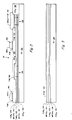
- Figure 1 includes a portion of a magnetoresistive memory 10. Part of bit cell line 12 is shown, including part of bit cell 14 and all of bit cell 16. Bit cells 14 and 16 are comprised of first and second ferromagnetic, magnetoresistive layers 18 and 20, separated by a magnetic exchange coupling barrier layer 22. Layer 22 will prevent the magnetic domains in layer 18 from coupling to the magnetic domains of layer 20. Generally layer 22 will be of a nonmagnetic material. The magnetization vectors of layers 18 and 20 are antiparallel. Layers 18, 20 and 22 form a "sandwich" structure which results in good "flux closure", i.e. the magnetic field lines due to the magnetization of layers 18 and 20 are primarily confined to a closed path within the strucure. Flux closure reduces demagnetizing effects due to the presence of free magnetic poles at the edges of the ferromagentic films and due to other nearby fields, and is important for the proper functioning of magnetic memories with densely packed cells.
- Layer 24 overlies the sandwich structure. It is comprised of a resistive material which will not short out the electrical properties of layer 18 and serves as an etch stop to protect layer 18 during processing.
- a sutiable material for layer 24 is nitrogen doped tantalum, TaN x , where x is, preferably, selected so that Ta is 65 to 85 percent, by atomic concentration, of the TaN x .
- the amount of N in the TaN may vary between 2% and 50%, by atomic concentration. In certain, unusual cases, the percent of N may even lie outside this range. Generally, for thinner layers 24, the percentage of N can vary more widely than for thicker layers 24.
- Other suitable materials for layer 24 are a mixture or compound of a metal and either nitrogen oxygen, where the mixture or compound will not diffuse into layer 18 during processing.
- layer 24 is a material whose dimensions and resistivity are such that less than half of electrical current flowing through the bit cell (or device) will flow solely within layer 24, and layer 24 will not diffuse into layer 20 during processing. Preferably, only a small percent of the signal current will flow solely within layer 24.
- Suitable materials for layers 18 and 20 are permalloy (e.g. a mixture of 65% Ni, 15% Fe and 20% CO) and TaN x for layers 22 and 24. Note that x can be a different value for each of layers 22 and 24. Typically each of layers 18, 20, 22 and 24 are on the order of one hundred to several hundred angstroms thick. A specific useful example would have a thickness of 150A for layers 18 and 20, 50A for layer 22, and 500A for layer 24.
- bit line 12 is narrowed (sometimes it is severed).
- Layer 24 is thicker over junctions 26 and 28 than over the bit cells. This is due to the process by which the cells are manufactured (see below).
- an electrical conductor 30 (such as TiW) is deposited over the thicker or raised portions of layer 24. If the junction is to serve as an electrical contact 32 to other components, such as a sense amplifier, a second metal (such as AlCu/TiW) overlays layer 30 (see junction 28).
- Bit cell line 12 will be formed in a substrate 34 (Si or GaAs) which typically has a covering layer 36 (Such as SiN3 for Si substrates).
- An insulating layer 38 (e.g. SiO2) covers all of structure 10 except for electrical contacts 32 at the ends of the bit lines formed from the second metal.
- Layer 38 is shown in cutaway as two strips in Figure 1 for clarity.
- Figure 2 shows the complete coverage of layer 38 in a sectional view.
- the memories' conductive word lines 40 and 42 lay transverse to and at the centre of each bit cell. Word lines 40 and 42 are formed from the second metal.
- the number of vias cut is greatly reduced, typically being limited to only the contact sites at the end of the bit lines. Without a second metal over intermediate bit cell junctions, the width of the bit cell line is reduced and cells can be packed more closely.
- bit cell lines are first etched and the vias subsequently etched, the electrical contact sites at the vias will be protected.
- Figure 3 shows an intermediate product of the process which produces the device of Figure 2.
- layers 18, 20, 22, 24 and 30 have been deposited or formed over the entire surface of structure 10.
- bit cell line 12 is then ion milled.
- a shorting bar mask will be used to mask the bit cell junctions.
- a first etch (wet or dry) removes layer 30 from the unmasked portion of structure 10. For most dry etches, this first etch will cut into layer 24 resulting in raised portions of layer 24 being formed under the mask (i.e. at the junction sites). If the first etch is wet, (e.g. hot H2O2/H2O) only layer 30 will be removed, resulting in pads of TiW at the junction sites.
- the surface profile topography of the upper surface of layer 24 (shown in Figure 2) will be substantially flat. That is, the maximum variation surface profile height will be less than 100A, and often only a few angstroms.
- the surface profile topography of the upper surface of layer 24 will not be flat - varying in height more than 100A and typically varying in height several thousand angstroms.
- the photoresist is stripped, layer 38 is deposited over all of structure 10 and the vias masked. A second etch forms the vias and exposes metal 30 at the selected locations.
- Second metal such as AlCu/TiW
- Another passivation layer typically covers all of device 10.
- the present invention has been specifically described with regard to a magnetoresistive memory, but it may be used advantageously as an etch barrier and to protect a layer from a processing atmosphere in other solid state devices.
Landscapes
- Engineering & Computer Science (AREA)
- Computer Hardware Design (AREA)
- Hall/Mr Elements (AREA)
- Semiconductor Memories (AREA)
- Measuring Magnetic Variables (AREA)
- Thin Magnetic Films (AREA)
Applications Claiming Priority (2)
| Application Number | Priority Date | Filing Date | Title |
|---|---|---|---|
| US07/008,211 US4754431A (en) | 1987-01-28 | 1987-01-28 | Vialess shorting bars for magnetoresistive devices |
| US8211 | 1987-01-28 |
Publications (3)
| Publication Number | Publication Date |
|---|---|
| EP0276784A2 true EP0276784A2 (de) | 1988-08-03 |
| EP0276784A3 EP0276784A3 (en) | 1990-04-11 |
| EP0276784B1 EP0276784B1 (de) | 1993-04-14 |
Family
ID=21730374
Family Applications (1)
| Application Number | Title | Priority Date | Filing Date |
|---|---|---|---|
| EP88100978A Expired - Lifetime EP0276784B1 (de) | 1987-01-28 | 1988-01-23 | Durchstossfreie Kurzschlussbruecken fuer magnetoresistive Anordnungen |
Country Status (4)
| Country | Link |
|---|---|
| US (1) | US4754431A (de) |
| EP (1) | EP0276784B1 (de) |
| JP (1) | JPH077592B2 (de) |
| DE (1) | DE3880163T2 (de) |
Families Citing this family (23)
| Publication number | Priority date | Publication date | Assignee | Title |
|---|---|---|---|---|
| US4945397A (en) * | 1986-12-08 | 1990-07-31 | Honeywell Inc. | Resistive overlayer for magnetic films |
| US4918655A (en) * | 1988-02-29 | 1990-04-17 | Honeywell Inc. | Magnetic device integrated circuit interconnection system |
| US5173873A (en) * | 1990-06-28 | 1992-12-22 | The United States Of America As Represented By The Administrator Of The National Aeronautics And Space Administration | High speed magneto-resistive random access memory |
| US5251170A (en) * | 1991-11-04 | 1993-10-05 | Nonvolatile Electronics, Incorporated | Offset magnetoresistive memory structures |
| US5420819A (en) * | 1992-09-24 | 1995-05-30 | Nonvolatile Electronics, Incorporated | Method for sensing data in a magnetoresistive memory using large fractions of memory cell films for data storage |
| US6256222B1 (en) | 1994-05-02 | 2001-07-03 | Matsushita Electric Industrial Co., Ltd. | Magnetoresistance effect device, and magnetoresistaance effect type head, memory device, and amplifying device using the same |
| US5841611A (en) * | 1994-05-02 | 1998-11-24 | Matsushita Electric Industrial Co., Ltd. | Magnetoresistance effect device and magnetoresistance effect type head, memory device, and amplifying device using the same |
| WO1995035507A1 (en) * | 1994-06-18 | 1995-12-28 | The University Of Sheffield | Magnetic field responsive device |
| US6081445A (en) * | 1998-07-27 | 2000-06-27 | Motorola, Inc. | Method to write/read MRAM arrays |
| US6343032B1 (en) | 1999-07-07 | 2002-01-29 | Iowa State University Research Foundation, Inc. | Non-volatile spin dependent tunnel junction circuit |
| US6317359B1 (en) | 1999-07-07 | 2001-11-13 | Iowa State University Research Foundation, Inc. | Non-volatile magnetic circuit |
| US6542000B1 (en) | 1999-07-30 | 2003-04-01 | Iowa State University Research Foundation, Inc. | Nonvolatile programmable logic devices |
| US6493259B1 (en) * | 2000-08-14 | 2002-12-10 | Micron Technology, Inc. | Pulse write techniques for magneto-resistive memories |
| US6724654B1 (en) * | 2000-08-14 | 2004-04-20 | Micron Technology, Inc. | Pulsed write techniques for magneto-resistive memories |
| US6693826B1 (en) | 2001-07-30 | 2004-02-17 | Iowa State University Research Foundation, Inc. | Magnetic memory sensing method and apparatus |
| US6545906B1 (en) * | 2001-10-16 | 2003-04-08 | Motorola, Inc. | Method of writing to scalable magnetoresistance random access memory element |
| US7095646B2 (en) | 2002-07-17 | 2006-08-22 | Freescale Semiconductor, Inc. | Multi-state magnetoresistance random access cell with improved memory storage density |
| US6956763B2 (en) | 2003-06-27 | 2005-10-18 | Freescale Semiconductor, Inc. | MRAM element and methods for writing the MRAM element |
| US6967366B2 (en) | 2003-08-25 | 2005-11-22 | Freescale Semiconductor, Inc. | Magnetoresistive random access memory with reduced switching field variation |
| US7129098B2 (en) | 2004-11-24 | 2006-10-31 | Freescale Semiconductor, Inc. | Reduced power magnetoresistive random access memory elements |
| US8657603B2 (en) * | 2011-04-27 | 2014-02-25 | Leslye Zina Solomon | System for compiling knitting/crocheting patterns into stepwise time-adjustable voice and visual instructions |
| US9082695B2 (en) | 2011-06-06 | 2015-07-14 | Avalanche Technology, Inc. | Vialess memory structure and method of manufacturing same |
| CN103637802A (zh) * | 2013-12-13 | 2014-03-19 | 绵阳市腾扬机电制品有限责任公司 | 一种磁共振医疗仪的磁体线圈骨架定位装夹装置 |
Family Cites Families (28)
| Publication number | Priority date | Publication date | Assignee | Title |
|---|---|---|---|---|
| NL231142A (de) * | 1957-10-23 | |||
| US3125743A (en) * | 1958-03-19 | 1964-03-17 | Nondestructive readout of magnetic cores | |
| US3160863A (en) * | 1961-12-18 | 1964-12-08 | Ibm | Magnetoresistive storage device |
| US3375503A (en) * | 1963-09-13 | 1968-03-26 | Ibm | Magnetostatically coupled magnetic thin film devices |
| US3461438A (en) * | 1964-04-06 | 1969-08-12 | Ibm | Memory element having two orthogonally disposed magnetic films |
| US3587069A (en) * | 1964-10-31 | 1971-06-22 | Zaidan Hojin Parametron Kenkyu | Ferromagnetic thin-film memory element and a method of recording information therein |
| US3452334A (en) * | 1964-12-28 | 1969-06-24 | Ibm | Magnetic film memories with an intermediate conductive element as a drive line return path |
| US3525023A (en) * | 1965-08-05 | 1970-08-18 | Sperry Rand Corp | Multilayer thin film magnetic memory element |
| FR1541255A (fr) * | 1966-12-07 | Ibm | Dispositif de mémoire associative | |
| US3524173A (en) * | 1967-05-22 | 1970-08-11 | Ampex | Process for electrodeposition of anisotropic magnetic films and a product formed by the process |
| US3701983A (en) * | 1969-12-19 | 1972-10-31 | Sylvania Electric Prod | Magnetostatically coupled thin-film magnetic memory devices |
| US3623038A (en) * | 1969-12-19 | 1971-11-23 | Gte Sylvania Inc | Pheral layer magnetic thin film element |
| US3701931A (en) * | 1971-05-06 | 1972-10-31 | Ibm | Gold tantalum-nitrogen high conductivity metallurgy |
| US3798623A (en) * | 1972-07-20 | 1974-03-19 | Sperry Rand Corp | Quad density solid stack memory |
| US3864751A (en) * | 1973-10-04 | 1975-02-04 | Ibm | Induced bias magnetoresistive read transducer |
| FR2276658A1 (fr) * | 1974-06-25 | 1976-01-23 | Tecsi | Poste de lecture pour un registre a propagation de domaines magnetiques sur une couche mince |
| JPS576962Y2 (de) * | 1974-07-26 | 1982-02-09 | ||
| US3908194A (en) * | 1974-08-19 | 1975-09-23 | Ibm | Integrated magnetoresistive read, inductive write, batch fabricated magnetic head |
| US4097802A (en) * | 1975-06-30 | 1978-06-27 | International Business Machines Corporation | Magnetoresistive field sensor with a magnetic shield which prevents sensor response at fields below saturation of the shield |
| US4024489A (en) * | 1975-11-18 | 1977-05-17 | International Business Machines Corporation | Magnetoresistive sandwich including sensor electrically parallel with electrical shunt and magnetic biasing layers |
| JPS5856243B2 (ja) * | 1976-09-09 | 1983-12-14 | 富士通株式会社 | バブル磁区用パ−マロイ膜の作成方法 |
| SU763964A1 (ru) * | 1978-07-13 | 1980-09-15 | Предприятие П/Я М-5769 | Датчик дл считывани цилиндрических магнитных доменов |
| US4208725A (en) * | 1979-02-23 | 1980-06-17 | Sperry Corporation | Magneto-resistive detector for cross-tie wall memory system |
| JPS55123183A (en) * | 1979-03-15 | 1980-09-22 | Nec Corp | Magnetic detector |
| US4356523A (en) * | 1980-06-09 | 1982-10-26 | Ampex Corporation | Narrow track magnetoresistive transducer assembly |
| JPS584992A (ja) * | 1981-07-01 | 1983-01-12 | Hitachi Ltd | 磁気電気変換素子 |
| JPS5999370A (ja) * | 1982-11-30 | 1984-06-08 | Copal Co Ltd | 磁気抵抗素子を具える磁気検出器の製造方法 |
| US4459321A (en) * | 1982-12-30 | 1984-07-10 | International Business Machines Corporation | Process for applying closely overlapped mutually protective barrier films |
-
1987
- 1987-01-28 US US07/008,211 patent/US4754431A/en not_active Expired - Lifetime
-
1988
- 1988-01-23 DE DE8888100978T patent/DE3880163T2/de not_active Expired - Lifetime
- 1988-01-23 EP EP88100978A patent/EP0276784B1/de not_active Expired - Lifetime
- 1988-01-28 JP JP63016012A patent/JPH077592B2/ja not_active Expired - Lifetime
Also Published As
| Publication number | Publication date |
|---|---|
| DE3880163D1 (de) | 1993-05-19 |
| JPH077592B2 (ja) | 1995-01-30 |
| JPS63301578A (ja) | 1988-12-08 |
| DE3880163T2 (de) | 1993-08-19 |
| EP0276784A3 (en) | 1990-04-11 |
| US4754431A (en) | 1988-06-28 |
| EP0276784B1 (de) | 1993-04-14 |
Similar Documents
| Publication | Publication Date | Title |
|---|---|---|
| EP0276784B1 (de) | Durchstossfreie Kurzschlussbruecken fuer magnetoresistive Anordnungen | |
| US4897288A (en) | Vialess shorting bars for magnetoresistive devices | |
| EP0271017B1 (de) | Magnetschicht-Speicherzelle oder -Detektor | |
| US4945397A (en) | Resistive overlayer for magnetic films | |
| US6635499B1 (en) | MRAM sense layer isolation | |
| US10381551B1 (en) | Spin orbit torque magnetoresistive random access memory containing shielding element and method of making thereof | |
| US6806546B2 (en) | Passivated magneto-resistive bit structure | |
| US6912107B2 (en) | Magnetic element with insulating veils and fabricating method thereof | |
| EP1038299B1 (de) | Magnetischer tunnelübergang mit geringer umschalt-feldstärke für magnetische mehrzustands-speicherzelle | |
| US6720597B2 (en) | Cladding of a conductive interconnect for programming a MRAM device using multiple magnetic layers | |
| US5956267A (en) | Self-aligned wordline keeper and method of manufacture therefor | |
| US5424236A (en) | Method for forming offset magnetoresistive memory structures | |
| US5569617A (en) | Method of making integrated spacer for magnetoresistive RAM | |
| EP1607980B1 (de) | Neue Abdeckstruktur zum Verbessern von dR/R einer MTJ-Vorrichtung | |
| US5966323A (en) | Low switching field magnetoresistive tunneling junction for high density arrays | |
| US20200006633A1 (en) | Spin orbit torque magnetoresistive random access memory containing shielding element and method of making thereof | |
| EP1207538B1 (de) | Magnetischer Direktzugriffspeicher mit verbesserterDurchbruchspannung | |
| WO2005024856A2 (en) | Method and system for providing a magnetic element including passivation structures | |
| US6780652B2 (en) | Self-aligned MRAM contact and method of fabrication | |
| US20020186583A1 (en) | Recessed magnetic storage element and method of formation | |
| EP0331051B1 (de) | Als integrierte Schaltung ausgebildetes Verbindungssystem für eine magnetische Anordnung | |
| WO2003056562A1 (en) | Magneto-electronic component for high density memory | |
| US7056749B2 (en) | Simplified magnetic memory cell |
Legal Events
| Date | Code | Title | Description |
|---|---|---|---|
| PUAI | Public reference made under article 153(3) epc to a published international application that has entered the european phase |
Free format text: ORIGINAL CODE: 0009012 |
|
| AK | Designated contracting states |
Kind code of ref document: A2 Designated state(s): DE FR GB NL |
|
| PUAL | Search report despatched |
Free format text: ORIGINAL CODE: 0009013 |
|
| AK | Designated contracting states |
Kind code of ref document: A3 Designated state(s): DE FR GB NL |
|
| 17P | Request for examination filed |
Effective date: 19901008 |
|
| 17Q | First examination report despatched |
Effective date: 19920214 |
|
| GRAA | (expected) grant |
Free format text: ORIGINAL CODE: 0009210 |
|
| AK | Designated contracting states |
Kind code of ref document: B1 Designated state(s): DE FR GB NL |
|
| REF | Corresponds to: |
Ref document number: 3880163 Country of ref document: DE Date of ref document: 19930519 |
|
| ET | Fr: translation filed | ||
| PLBE | No opposition filed within time limit |
Free format text: ORIGINAL CODE: 0009261 |
|
| STAA | Information on the status of an ep patent application or granted ep patent |
Free format text: STATUS: NO OPPOSITION FILED WITHIN TIME LIMIT |
|
| 26N | No opposition filed | ||
| REG | Reference to a national code |
Ref country code: GB Ref legal event code: IF02 |
|
| REG | Reference to a national code |
Ref country code: FR Ref legal event code: TP |
|
| REG | Reference to a national code |
Ref country code: GB Ref legal event code: 732E |
|
| NLS | Nl: assignments of ep-patents |
Owner name: MICRON TECHNOLOGY, INC. |
|
| PGFP | Annual fee paid to national office [announced via postgrant information from national office to epo] |
Ref country code: NL Payment date: 20070103 Year of fee payment: 20 |
|
| PGFP | Annual fee paid to national office [announced via postgrant information from national office to epo] |
Ref country code: GB Payment date: 20070117 Year of fee payment: 20 |
|
| PGFP | Annual fee paid to national office [announced via postgrant information from national office to epo] |
Ref country code: DE Payment date: 20070118 Year of fee payment: 20 |
|
| REG | Reference to a national code |
Ref country code: GB Ref legal event code: PE20 |
|
| NLV7 | Nl: ceased due to reaching the maximum lifetime of a patent |
Effective date: 20080123 |
|
| PG25 | Lapsed in a contracting state [announced via postgrant information from national office to epo] |
Ref country code: NL Free format text: LAPSE BECAUSE OF EXPIRATION OF PROTECTION Effective date: 20080123 |
|
| PGFP | Annual fee paid to national office [announced via postgrant information from national office to epo] |
Ref country code: FR Payment date: 20070109 Year of fee payment: 20 |
|
| PG25 | Lapsed in a contracting state [announced via postgrant information from national office to epo] |
Ref country code: GB Free format text: LAPSE BECAUSE OF EXPIRATION OF PROTECTION Effective date: 20080122 |