EP0275362A2 - Safety control system - Google Patents
Safety control system Download PDFInfo
- Publication number
- EP0275362A2 EP0275362A2 EP87113354A EP87113354A EP0275362A2 EP 0275362 A2 EP0275362 A2 EP 0275362A2 EP 87113354 A EP87113354 A EP 87113354A EP 87113354 A EP87113354 A EP 87113354A EP 0275362 A2 EP0275362 A2 EP 0275362A2
- Authority
- EP
- European Patent Office
- Prior art keywords
- signal processing
- signal
- trip
- sensors
- processing channels
- Prior art date
- Legal status (The legal status is an assumption and is not a legal conclusion. Google has not performed a legal analysis and makes no representation as to the accuracy of the status listed.)
- Granted
Links
Images


Classifications
-
- G—PHYSICS
- G06—COMPUTING; CALCULATING OR COUNTING
- G06F—ELECTRIC DIGITAL DATA PROCESSING
- G06F11/00—Error detection; Error correction; Monitoring
- G06F11/07—Responding to the occurrence of a fault, e.g. fault tolerance
- G06F11/16—Error detection or correction of the data by redundancy in hardware
- G06F11/18—Error detection or correction of the data by redundancy in hardware using passive fault-masking of the redundant circuits
- G06F11/183—Error detection or correction of the data by redundancy in hardware using passive fault-masking of the redundant circuits by voting, the voting not being performed by the redundant components
- G06F11/184—Error detection or correction of the data by redundancy in hardware using passive fault-masking of the redundant circuits by voting, the voting not being performed by the redundant components where the redundant components implement processing functionality
- G06F11/185—Error detection or correction of the data by redundancy in hardware using passive fault-masking of the redundant circuits by voting, the voting not being performed by the redundant components where the redundant components implement processing functionality and the voting is itself performed redundantly
-
- G—PHYSICS
- G05—CONTROLLING; REGULATING
- G05B—CONTROL OR REGULATING SYSTEMS IN GENERAL; FUNCTIONAL ELEMENTS OF SUCH SYSTEMS; MONITORING OR TESTING ARRANGEMENTS FOR SUCH SYSTEMS OR ELEMENTS
- G05B9/00—Safety arrangements
- G05B9/02—Safety arrangements electric
- G05B9/03—Safety arrangements electric with multiple-channel loop, i.e. redundant control systems
Abstract
Description
- The present invention generally relates to a safety control system such as for a nuclear power plant, and more particularly to a safety control system provided with two independent actuating means.
- In nuclear power plants, it is a common practice to provide the plant with a safety and safeguard system for protecting the plant as well as a nuclear reactor against any possible abnormal transients and other unwanted phenomena for the purpose of assuring the safety of the nuclear reactor. By way of example, Japanese Laid-open Patent publication No. 118801/1986 (JP-A 61-118801) corresponding to U.S. Patent Application No. 666,696 filed October 30, 1984 discloses a nuclear reactor safety and protection or safeguard system which includes sensors and channel signal processors connected in series, respectively, in a quadruple array and two logic circuits to which the outputs of the four channel signal processors are inputted. Each of the logic circuits is implemented in the form of two-out-of-four (2-out-of-4) voting logic circuit configuration, where one of the logic circuits is destined to produce a signal for activating a protecting system which can respond to the signal by opening a circuit breaker inserted in an electric power supply line leading to an electromagnetic device incorporated in a control rod controller unit to thereby scram the reactor, while the other logic circuit is designed to produce another safety system activating signal which brings about operation of an emergency borated water injection system and a spray system installed within a containment vessel of the reactor.
- In connection with the 2-out-of-4 voting logic, typical examples thereof are found in a Japanese publication entitled "Nuclear Power Handbook", (1976), p.p. 263-267 and in particular on page 264, Table 9.6.
- The aforementioned Japanese patent publication thus teaches the use of logic circuits implemented in the form of a 2-out-of 4 voting logic. However, no concrete circuit configuration of the 2-out-of-4 logic circuit is disclosed in this publication, although the abovementioned handbook shows in the Table 9.6 a typical example of the configuration of the 2-out-of-4 logic circuit.
- More specifically, the Japanese Laid-open Patent Publication No. 118801/1986 concerns a safety control safeguard system for a pressurized water reactor (PWR). According to the safety control safeguard system for the reactor disclosed in this publication, one of the 2-out-of-4 logic circuits is utilized for activating the coil or solenoid incorporated in the control rod controller unit. In this conjunction, it is however noted that in the case of a control rod drive controller unit provided for assuring the safety of a boiling water reactor (BWR) known heretofore, the scramming electromagnetic valve for operating the controller unit is equipped with a pair of excitation coils. Consequently, according to the teachings disclosed in the Japanese patent publication mentioned above, the 2-out-of-4 logic circuit has to be provided for each of the excitation coils. For implementing the 2-out-of-4 logic circuit, the circuit configuration shown in the Table 9.6 on page 264 of the aforementioned handbook may be adopted.
- Needless to say, when two independent manipulating or actuating means are provided for a single control system in concern (e.g. when two independent excitation coils are provided as in the case of the BWR), the two-out-of-four logic circuit has to be provided for each of the actuating means for activation thereof, which in turn means that the structure of the safety control safeguard system becomes very complicated, to disadvantage.
- It is an object of the present invention to provide a control system of a simplified structure.
- Another object of the present invention is to provide a control system which includes two-out-of-four logic circuits having no common mode therebetween and which can enjoy a significantly improved reliability.
- A further object of the present invention is to provide a control system in which status signal processor or maintenance signal processor which suffers abnormality can be easily disconnected.
- In view of the above objects, there is provided according to an aspect of the present invention a control system which comprises sensors disposed in a quadruple array, first, second, third and fourth signal processing channels disposed in parallel and each including signal processing means having an input supplied with an output signal from the associated sensor, two independent actuating means, an apparatus of which operation is controlled by the actuating means, and switch means communicated with the first, second, third and fourth signal processing channels and activiating operation of the two independent actuating means in response to the inputting of a trip signal produced in response to at least two outputs of the signal processing channels.
- By virtue of the inventive arrangement in which the switch means for the control system is so arranged as to operate the two independent actuating means in response to the trip signals produced from at least two of four signal processing channels and constitutes in cooperation with the two actuating means a two-out-of-four logic circuit, the system structure can be significantly simplified.
-
- Fig. 1 is a view showing a general arrangement of a safety control safeguard system according to a preferred embodiment of the present invention;
- Fig. 2 is a view showing an exemplary configuration of a switching circuit employed in the system shown in Fig. 1;
- Figs. 3, 4, 5, 6 and 7 are views showing other embodiments of the safety control safeguard system according to the present invention;
- Figs. 8 and 9 are views showing circuit configurations of a power circuit according to further embodiment of the invention;
- Fig. 10 is a view showing an arrangement of a signal processor according to another embodiment of the present invention;
- Fig. 11 is a view for illustrating processing procedure executed by the signal processor shown in Fig. 10; and
- Fig. 12 is a view for illustrating another processing procedure corresponding to a version of the procedure illustrated in Fig. 11.
- Now, referring to the accompanying drawings, the control safeguard system according to the invention will be described in detail in conjunction with the preferred or exemplary embodiments on the assumption that the invention is applied to the safety control for a nuclear reactor plant.
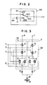
- First referring to Figs. 1 and 2, the nuclear reactor safety control safeguard system according to an embodiment of the invention is composed of four
signal processing channels 25A to 25D each including one signal processor, one switching circuit and one diagnosis circuit. (By way of example, thesignal processing channel 25A comprises asignal processor 1, aswitching circuit 19A and adiagnosis circuit 22A.) In each of the signal processing channels, the signal processor is connected to a number of sensors. More specifically, in the case of thechannel 25A, thesignal processor 1 is connected to the sensors A₁ to N₁. In thesignal processing channel 25B, thesignal processor 2 is connected to the sensor A₂ to N₂. In thesignal processing channel 25C, thesignal processor 3 is connected to the sensor A₃ to N₃. Finally in thesignal processing channel 25D, thesignal processor 4 is connected to the sensor A₄ to N₄. In this connection, it should be mentioned that a quartet of the sensors designated by a same alphabetic character (e.g. the sensors A₁, A₂, A₃ and A₄) are disposed at positions close to one another for measuring a same type of status quantity (hereinafter referred to as the same type status quantity). On the other hand, the sensors labeled with different alphabetic characters are destined to measure status quantities differing in nature from one another or a same status quantity at different locations (hereinafter referred to as the different types of status quantities). In the case of the illustrative embodiment of the invention under consideration, four sensors are provided for measuring one type status quantity. It should however be understood that one sensor may be provided for measuring one type status quantity and the sensor output signal may be inputted to thesignal processors 1 to 4 of the four signal processing channels, respectively. Thesignal processors processing channels 25A to 25D produce trip signals a to d for scramming the nuclear power plant. - The
switching circuit 19A may be composed of a change-over switch 20 and apower supply source 21, as exemplified by the circuit configuration shown in Fig. 2. The change-overswitch 20 includesstationary contacts movable contact 20D closed constantly to the stationary contact terminal 20C. Thepower supply source 21 is connected to thestationary contact 20B. Theswitching circuit switching circuit 19A. Thestationary contacts 20A of theswitching circuits 19A to 19D are connected to the output terminals of thesignal processors 1 to 4, respectively. So long as thesignal processors 1 to 4 function in the normal state, themovable contacts 20D of theswitching circuits 19A to 19D remain closed to the respectivestationary contacts 20A. - Turning back to Fig. 1, the power circuit (constituting the switch means) 5 includes a first switch portion (also referred to as the first switch circuitry) 5A and a second switch portion (also referred to as the second switch circuitry) 5B. Each of the
switch circuitries circuitry 5A,relays relays 10 and 11 is connected in series to therelay 9. Therelay 8 is connected to thepower supply source 6. In thesecond switch circuitry 5B,relays relays relay 13. The power supply source 7 is connected to therelay 12. Therelays 8 to 15 havemovable contacts 8A to 15A andstationary contacts 8B to 15B, respectively. - The
relays changeover circuit 19A to receive the trip signal a for activating therelays relays signal switching circuit 19B for receiving the trip signal b serving for activation of these relays. In a similar manner,relays signal switching circuit 19C for receiving the trip signal c while therelays 11 and 13 are connected to the stationary contact terminal 20C of thesignal switching circuit 19D for receiving the trip signal d serving for the relay activation. So long as the operation of the nuclear power plant is normal, themovable contacts 8A to 15A remain in the state closed to thestationary contacts 8B to 15B, respectively. - The common output terminal of the
relays 10 and 11 (the output terminal of theswitch circuitry 5A) is connected to anexcitation coil 16 of ascramming electromagnet 18. On the other hand, the common output terminal of therelays 14 and 15 (the output terminal of theswitch ricuitry 5B) is connected to theother excitation coil 17 of thescramming electromagnet 18. Thescramming electromagnet 18 is incorporated in a scrammingelectromagnetic valve 19. - In Fig. 1,
reference characters 22A to 22D denote, respectively, abnormality diagnosis units for making determination as to the presence or absence of abnormality in the associatedsignal processors 1 to 4, respectively. - In the case of the embodiment of the invention now under consideration, the
relays 8 to 15 of thepower circuit 5 cooperate with theexcitation coils switch circuitry 5A, theexcitation coil 16 connected thereto, theswitch circuitry 5B and theexcitation coil 17 constitute a sort of the 2-out-of-4 logic circuit. - Assuming now that the
signal processors 1 to 4 which are normally operating produce the trip signals a to d (indicating some abnormal state in the plant), themovable contacts movable contacts movable contacts 11A and 15A being opened in response to the trip signal d, resulting in that both of the excitation coils 16 and 17 are deenergized. Upon deenergization of both the excitation coils 16 and 17, the scrammingelectromagnet 18 is energized to open the scrammingelectromagnetic valve 19. Consequently, the control rod drive unit (not shown) operates to insert rapidly the control rods into the reactor core to scram the reactor. - Thus, it will be appreciated that the 2-out-of-4 logic circuit according to the illustrative embodiment of the present invention is so designed as to implement the 2-out-of-4 voting function with preference being put to "0" in the sense that the movable contacts of the
relays 8 to 15 are opened in response to the signal input of logic "0". - In the case of the instant embodiment, it is assumed that the signal scramming
electromagnetic valve 19 is employed. However, it should be understood that the concept of the present invention incarnated in the instant embodiment can be equally applied to such arrangement in which a plurality of scrammingelectromagnetic valves 19 are provided and thepower circuits 15 are correspondingly connected to the scrammingelectromagnetic valves 19, respectively, wherein the output signals of the switchingcircuits 19A to 19D are applied in parallel to the power circuits, respectively, to thereby bring about the scramming operation. Additionally, although it has been described that the scrammingelectromagnetic valve 19 to be driven is equipped with the pair of excitation coils in the arrangement shown in Fig. 1, the concept of the invention can be also applied to the case where two scramming electromagnetic valves each having one excitation coil are connected in series to each other. It should be added here that the scramming electromagnetic valve is provided in an air pipe for actuating pnewmatically an open/close valve disposed on the exit side of a scramming accumulator of the control rod drive unit. - Turning to Fig. 1, energization and deenergization of the
excitation coil 16 are controlled by theswitch circuitry 5A while energization and deenergization of theexcitation coil 17 is controlled by theswitch circuitry 5B. In this conjunction, when the signal effective to set theexcitation coil 6 to the deenergized state is represented by A with the signal effective for deenergizing theexcitation coil 17 by B, the following relations apply valid between these signals A and B. A = ab(c + d) ..... (1)
B = dc(a + d) ..... (2)
- When the scram signal, applied to the scramming
electromagnetic valve 19 is represented by Z, this signal is given by
Z = A + B ..... (3)
By substituting the expressions (1) and (2), the expression (3) can be rewritten as follows:
Z = abc + bcd + cda + dab ..... (4) - From the expression (4), it is apparent that when any two of the trip signals a, b, c and d are logic "0", then the scram signal Z assumes always logic "0" even when the other trip signals are logic "1". Thus, there can be realized the nuclear reactor safety control safeguard system which is operative based on the 2-out-of-4 logic with preference or priority put to the logic level "0". Parenthetically, the number of the relays incorporated in the
power circuit 5 is eight. However, since such arrangement is sufficient that two relays can be operated by one trip signal (e.g. therelays - In the reactor safety control safeguard system of the arrangement described above, there may arise such situation in which one of the signal processors is failed for some reason or disconnected for the purpose of maintenance. In such case, it is then possible to realize a 2-out-of-3 logic function with the remaining three processors, as will be described below.
- The abovementioned advantageous feature can be attained by constituting one signal processing channel with the signal processor, the switching circuit and the abnormality diagnosis circuit. More specifically, it is assumed, by way of example, that the
diagnosis circuit 22A having the input supplied with the status signal of thesignal processor 1 decides on the basis of the input signal that some abnormality occurs in the associatedsignal processor 1. Then, thediagnosis circuit 22A produces a corresponding command signal which causes themovable contact 20D of the change-over switch 20 of theswitching circuit 19A to be detached from thestationary contact 20A and closed to thestationary contact 20B. The power supply source produces a signal of logic "1". The relay supplied with the logic "1" signal from thepower source 21 of the switching circuit maintains the movable contact in the closed state. In this way, the signal of logic "1" is produced by the change-over operation of the switching circuit connected to the signal processor which is in the abnormal state, whereby the 2-out-of-3 logic can be realized with the other three signal processors operating normally. Themovable contact 20D of the change-over switch 20 of the switching circuit is constantly in contact with thestationary contact 20A, so long as the signal processor to which the aforementioned switching circuit is connected operates normally. The switching circuit is so arranged that when abnormality occurs in the operation of the associated signal processor which may produce a false trip signal to thepower circuit 5, themovable contact 20D of the switching circuit is closed to thestationary contact 20B, whereby the signal of logic "1" is forcibly supplied to thepower circuit 5. The change-over switch 20 may be controlled through manipulation of operator (not illustrated) or automati cally in response to the command issued by the diagnosis unit. It should be mentioned that the diagnosis unit may be realized by any appropriate circuit known heretofore (reference may be made, for example, to JP-A 59-51393 and U.S. Patent Application No. 402,053 filed July 27, 1982). - Disconnection of the signal processor will now be described in conjunction with the
processor 1, by way of example. When thesignal processor 1 assumes the abnormal state, the diagnosis unit issues a command signal, in response to which themovable contact 20D of the change-over switch 20 of theswitching circuit 19A is changed over from thestationary contact 20A to thestationary contact 20B. At the moment themovable contact 20D is changed over to thestationary contact 20B from thestationary contact 20A, chattering will take place in the change-over switch 20, resulting in that the output signal appearing at the terminal 20C may vary from logic "0" to "1" and vice versa. However, since the 2-out-of-4 logic configuration is realized by thepower circuit 5 and the excitation coils 16 and 17, the nuclear reactor will never be erroneously scrammed due to the chattering. The voltage value of thepower source 21 to which thestationary contact 20B is connected is thus outputted as the logic "1" signal. Consequently, the signal a outputted from the switchingcircuit 19A assumes the logic level "1". By placing the value of this signal a into the expression (4), the scramming signal Z can be given by
Z = bc + cd + db ..... (5) - As will be seen from the above expression (5), the output signal of the
switching circuit 19A belonging to thesignal processing channel 25A is forcibly caused to assume the logic "1" level upon disconnection of thesignal processor 1, as the result of which the 2-out-of-3 logic function can be realized for the output signals from the remainingsignal processors - The forgoing description has been based on the assumption that the
signal processor 1 shown in Fig. 1 is to be disconnected. However, the same applies valid for the disconnection of theother signal processor signal processor 2 is disconnected, theswitching circuit 19B is so controlled that the signal b assumes logic "1". Then, from the expression (4), the scram signal Z is given by
Z = ac + cd + da ..... (6) - When the
signal processor 3 is to be disconnected, the switchingcircuit 19C is so controlled that the signal c assumes the logic level "1". Then, from the expression (4), the scram signal Z is given by
Z = ab + bd + da ..... (7) - Finally, when the
signal processor 4 is disconnected, theswitching circuit 19D is so controlled that d = "1". From the expression (4), the scram signal Z is then given by
Z = ab + bc + ca ..... (8) - In any case, when one of the signal processors is disconnected, the output signal of the relevant signal processing channel can be forcibly set to logic "1", whereby the 2-out-of-3 voting logic can be realized to enhance significantly the reliability of the reactor safety control safeguard system.
- With the reactor safety control safeguard arrangement described above, there can be accomplished advantageous features such as mentioned below. Because the excitation coil 16 (first actuating means) and the excitation coil 17 (second actuating means) provided independent of each other for operating the scramming electromagnetic valve (the apparatus to be controlled) can cooperate with the
power circuit 5 serving as the switch unit for operating the abovementioned excitation coils to constitute the 2-out-of-4 logic circuit, the structure of the switch unit power circuit 5) can be significantly simplified, which in turn contributes to enhancement of the reliability of the safety control safeguard system for the nuclear reactor. Additional advantage may be seen in that the 2-out-of-4 logic configuration can be realized without need for modifying the arrangement of the existing electromagnetic valve having two excitation coils or the one having one excitation coil in the operating nuclear plant. Besides, when one of the four channel signal processors is disconnected due to failure or for the maintenance purpose, the 2-out-of-4 logic configuration is rearranged to the 2-out-of-3 logic which can positively prevent the safeguard system from operating erroneously or from remaining inoperative. Thus, there has been provided a nuclear reactor safety control safeguard system which can enjoy remarkably improved reliability. - Since the
power circuit 5 of the safety control safeguard system shown in Fig. 1 is constituted by first andsecond switch circuitries switch circuitries - Since each signal processing channel includes the switching circuit, the signal processor suffering from any abnormality or the signal processor which is to undergo maintenance procedure can be easily disconnected from the nuclear reactor safety control safeguard system, whereby the latter can be protected against any adverse influence otherwise possibly exerted by the signal processor to be disconnected.
- By virtue of provision of the abnormality diagnosis unit, the presence or absence of abnormality in the signal processors can be constantly monitored.
- Figs. 3 and 4 show other embodiments of the invention which are primarily directed to the circuit configurations around the power circuit. The nuclear reactor safety control safeguard systems according to the embodiments shown in Figs. 3 and 4 differ from the one described in the foregoing in respect to the manner in which the relays and the switching circuits are interconnected, but the other structural arrangement including those portions not shown remain same as in the case of the embodiment shown in Fig. 1. In any case, the
power circuit 5 and the excitation coils 16 and 17 cooperate to realize the 2-out-of-4 voting logic function. - First, the embodiment shown in Fig. 3 will be considered. The individual relays of the
switch circuitries relays switching circuit 19C for receiving, the trip signal c as the input thereto, and the realsy 10 and 12 are connected to the output terminal 20C of theswitching circuit 19B for receiving the trip signal b. Thus, in theswitch circuitry 5A, therelay 8 operates in response to the trip signal a, therelay 9 responds to the trip signal c in its operation, therelay 10 responds to the trip signal b, and the relay 11 reponds to the trip signal d. On the other hand, in theswitch circuitry 5B, therelay 12 responds to the trip signal b in its operation, therelay 13 responds to the trip signal d, therelay 14 responds to the trip signal a and therelay 15 responds to the trip signal c. Energization and deenergization of theexcitation coil 16 are controlled by theswitch circuitry 5A, while theexcitation coil 17 is under control of theswitch circuitry 5B in respect to its energization and deenergization. Consequently, the scram signal Z applied to the scrammingelectromagnetic valve 19 is given by
Z = ac(b + d) + bd(a + c) ..... (9)
= abc + bcd + cda + dab .....(10) - As will be seen from the expression (10), the scram signal Z is produced in accordance with the 2-out-of-4 logic as in the case of the scram signal defined by the expression (4) mentioned hereinbefore. Accordingly it will be readily appreciated that the embodiment shown in Fig. 3 can exhibit the actions and effects equivalent to those of the system shown in Fig. 1.
- Next, the embodiment shown in Fig. 4 will be considered. The individual relays of the
switch circuitries circuit 19 are connected in the manner mentioned below. Therelays switching circuit 19B for receiving the trip signal b as the input signal, while therelays switching circuit 19A for receiving the trip signal a. Accordingly, in theswitch circuitry 5A, therelay 8 operates in response to the trip signal b, therelay 9 operates in response to the trip signal c, therelay 10 responds to the trip signal a and the relay 11 operates in response to the trip signal d. Similarly, in theswitch circuitry 5B, therelay 12 responds to the trip signal a therelay 13 responds to the trip signal d, therelay 14 responds to the trip signal b and therelay 15 responds to the trip signal c in their operations, respectively. Consequently, theexcitation coil 16 is controlled by theswitch circuitry 5A with respect to its energization and deenergization with theexcitation coil 17 being controlled by theswitch circuitry 5B. Accordingly, the scram signal Z applied to the scrammingelectromagnetic valve 19 is given by
Z = bc(a + d) + ad(b + c) ..... (11)
= abc + bcd + cda + dab ..... (12) - As is apparent from the expression (12), the scram signal Z is produced in accordance with the 2-out-of-4 voting logic as in the case of the signal Z defined by the expression (4) mentioned hereinbefore. Thus, it will be appreciated that the system shown in Fig. 4 can exhibit advantageous actions and effects equivalent to those of the system shown in Fig. 1.
- Fig. 5 shows another embodiment of the present invention applied to a reactor main steam isolating system which is one of the nuclear reactor safety control systems. In particular, this figure shows a circuit arrangement of the power circuit generally denoted by
reference numeral 26 and associated parts. As is known in the art, the reactor main steam isolating system is employed for interrupting the flow of main steam supplied from a nuclear reactor through operation of anelectromagnetic valve 29. - The reactor main steam isolating system according to the illustrative embodiment shown in Fig. 5 differs from the system shown in Fig. 1 in that the
relays switch circuitries power supply source 28, while the output ends of theswitch circuitries power circuit 26 is implemented in the form of a 2-out-of-4 logic circuit. The junction between the output ends of theswitch circuitries excitation coil 27 of theelectromagnet 18 for theelectromagnetic valve 29. When a signal for setting theexcitation coil 27 to the deenergized state (this signal is the same as the one of operating the electromagnetic valve 29) is represented by Y, this signal Y is given by
Y = ab(c + d) + cd(a + b) ..... (13)
= abc + bcd + cda + dab ..... (14) - As will be seen from the expression (14), the signal Y is also produced in accordance with the 2-out-of-4 logic function similarly to the signal defined by the expression (4). It will thus be appreciated that the embodiment shown in Fig. 5 performs operation identical with that of the system shown in Fig. 1. Further, it should be mentioned that the
switch circuitries switch circuitries switch circuitries - When one of the signal processors is disconnected by controlling the switching circuit connected to the output side of the signal processor so that the logic "1" signal is produced, the other signal processor remaining connected are automatically rearranged to the 2-out-of-3 logic configuration, whereby very high reliability of the system can be assured.
- It will be readily understand that the amount of hardware resource as required is substantially same as in the case of the hitherto known system.
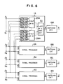
- Fig. 6 shows a reactor safety control safeguard system according to still another embodiment of the present invention. This embodiment differs from the one shown in Fig. 1 in that the
signal processors 1 to 4 are replaced byprocessors processors switch circuitries - The signal processor 1A includes digital trip modules DTM-N4 connected to the sensors A₁ to A₄, ..., N₁ to N₄, respectively. The digital trip modules DTM-N4 are connected to the sensors N₁ to N₄ serving for measuring a same type status quantity, while the digital trip modules DTM-N1 to DTM-N4 are connected to the sensors N₁ to N₄ for measuring another same type status quantity. The four digital trip modules having a same type status quantity inputted thereto (e.g. the digital trip modules DTM-A1 to DTM-A4) are set into the group. Accordingly, the number of groups each constituted by the four digital trip modules corresponds to the nuclear of the different type status quantities to be measured. For each of the groups, a 2-out-of-4 logic circuit is provided, wherein the output ends of the four digital trip modules belonging to one group are connected to one 2-out-of-4 logic circuit. More specifically, the digital trip modules DTM-A1 to DTM-A4 are connected to the 2-out-of-4
logic circuit 29A, the digital trip modules DTM-N1 to DTM-N4 are connected to the 2-out-of-4logic circuit 29N and so forth. Each of the 2-out-of-4logic circuits 29A, ..., 29N may be constituted, for example, by thepower circuit 26 shown in Fig. 5. The number of the 2-out-of-4 logic circuits incorporated in one signal processor is equal to n in the case of the embodiment under consideration. The n 2-out-of-4logic circuits 29A, ..., 29N belonging to the signal processor 1A are connected to a 1-out-of-n logic circuit 30. Theother signal processors n logic circuits 30 of the signal processors 1A to 4A are connected to the associatedswitching circuitries - Each digital trip module of each signal processor receives the status quantity signal outputted by the associated sensor and produces a trip signal when the sensor signal exceeds a predetermined value. Each of the 2-out-of-4 logic circuits incorporated in the processor produces the trip signal when at least two of the four digital trip modules belonging to one associated group outputs the trip signals. On the other hand, the 1-out-of-
n logic circuit 30 produces in the trip signal (i.e. trip signal a, b, c, or d) when at least one of n 2-out-of-4logic circuits 26A to 26N outputs the trip signal. The trip signals a, b, c, and dare effective to open the associated relays of the power circuit to deenergize the excitation coils 16 and 17 as in the case of the embodiment shown in Fig. 1. Consequently, the electromagnet: 18 becomes operative to open the scrammingelectromagnetic valve 19 for scramming the nuclear reactor. - The embodiment shown in Fig. 6 can exhibit same effects as those of the system shown in Fig. 1. Additionally, since the 2-out-of-4 logic circuits are employed in the signal processors 1A to 4A, the latter can enjoy high reliability.
- In a version of the system shown in Fig. 6, the digital trip modules DTM-A1 to DTM-A4, ..., DTM-N1 to DTM-N4 may be separated from the associated
signal processors logic circuits 29A, ..., 29N and the 1-out-of-n logic circuit 30. This modified system provides substantially same advantageous effects as those attainable in the system shown in Fig. 6. - Fig. 7 shows another modification of the system shown in Fig. 6. In the case of this modified system, the digital trip modules DTM-A1 to DTM-A4, ..., DTM-N1 to DTM-N4 are provided separately from the associated signal processors and disposed in the vicinity of the associated sensors A₁ to A₄, ..., N₁ to N₄ to be connected thereto, respectively. The digital trip module DTM-A1 to DTM-A4, ..., DTM-N1 to DTM-N4 are constituted by discrete microprocessors, respectively. The digital trip modules DTM-A1 to DTM-A4, ..., DTM-N1 to DTM-N4 are provided in the same number as the sensor groups A₁ to A₄, ..., N₁ to N₄ and thus reduced in number to 1/4 of the number of the digital trip modules employed in the system shown in Fig. 6 as well as the aforementioned version thereof. The signal processor 1B in the system shown in Fig. 7 is constituted by a microprocessor and incorporates the 2-out-of-4
logic circuits 29A, ..., 29N and a 1-out-of-n logic circuit 30. Each of theother signal processors - In contrast to the system described hereinbefore in conjunction with Fig. 6 and others in which the output signal of any given one sensor is divided so as to be inputted to the digital trip modules associated with the four signal processors, respectively, the output of any given one of the digital trip module is divided so as to be inputted to one 2-out-of-4 logic circuit incorporated in each of the four
signal processors - The system shown in Fig. 7 can assure similar effects to those of the system shown in Fig. 6. Besides, the embodiment shown in Fig. 7 can exhibit novel effects such as mentioned below. In most cases, the sensor signal is in the form of a current signal. Consequently, when the output of one sensor is branched into four channels, it is required that the four channel wires necessitated by the division of the sensor output be wound in loop, involving thus complicated wiring. However, in the case of the system shown in Fig. 7, the output of one sensor is not divided or branched but the output of one digital trip module to which the one sensor output is applied is branched into four channels. Consequently, the loop winding of the wiring conductors is not required on the output sides of the sensors and the digital trip modules, whereby the wiring can be significantly simplified. This arrangement is allowed because the output of the digital trip module assumes the form of a voltage signal in addition to the non-division of the sensor output. Additionally, since the number of the digital trip modules can be decreased considerably, the system shown in Fig. 7 can be realized in a very simplified structure.
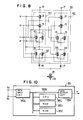
- Fig. 8 shows a further modification of the power circuit shown in Fig. 1 which has been developed on the basis of the various embodiments described in the foregoing.
- Referring to Fig. 8, the
power circuit 5C includes aswitch circuitry 5D corresponding to theswitch circuitry 5A of thepower circuit 5 shown in Fig. 1 but added withrelays switch circuitry 5E corresponding to the one 5B shown in Fig. 1 except that relays 33 and 34 are additionally provided. More specifically, the input ends of therelays relays 10 and 11 connected in parallel. The common output end of therelays excitation coil 16. The input ends of therelays 33 and 34 are also connected together while the output ends of therelays - Although one shown in detail. the
relays switching circuit 19A of asignal processing channel 25A for receiving the trip signal a as the input signal. Therelays switching circuit 19B of thesignal processing channel 25B for receiving the trip signal b. Further, therelays switching circuit 19C of thesignal processing channel 25C for receiving the trip signal c while therelays switching circuit 19D of thesignal processing channel 25D for receiving the trip signal d as the input signal. - When the scram signal applied to the scramming
electromagnetic valve 19 is represented by Z, the scram signal Z is given by
Z = ab(c + d)(a + b) + cd(c + d)(a + b)
= ab(c + d) + cd(a + b)
= abc + bcd + cda + dab ..... (15) - As will be appreciated from the expression (15), the power circuit shown in Fig. 8 is implemented in a 2-out-of-4 logic configuration in which preference is put on logic "0" as in the case of the embodiments described hereinbefore. Since the
switch circuitries power circuit 5C can be further improved. By way of example, even when therelays excitation coil 16 can be deenergized so far as therelays relays - Description will be made on a
power circuit 5F shown in Fig. 9. Thispower circuit 5F comprises a pair of switch circuitries each of whic is implemented in the same configuration as thepower circuit 26 shown in Fig. 5. The output end of theswitch circuitry 26A (i.e. the output ends of therelays excitation coil 16, while the output end of theswitch circuitry 26B (i.e. the output ends of therelays excitation coil 17. Theswitch circuitry 26B includes eightrelays 40 to 47 which are interconnected in the similar relation to therelays 8 to 15 of thepower circuit 26 shown in Fig. 5. Theswitch circuitry 26A also includes eightrelays 8 to 15 which are interconnected in the same manner as the relays of thepower circuit 26. Therelays power supply source 6 with therelays - The scram signal Z produced by the
power circuit 5F is given by
Z = ab(c + d) + cd(a + b) + ab(c + d) + cd(c + d)
= ab(c + d) + cd(a + b)
= abc + bcd + cda + dab ..... (16) - As can be seen from the expression (16), the
power circuit 5F shown in Fig. 9 is realized as the 2-out-of-4 voting logic configuration with preference put on the logic "0" as in the case of the various embodiments described so far. Thiscircuit 5F can assure a much improved reliability due to the circuit arrangement of theswitch circuitries switch circuitries switch circuitries power circuit 5E, no intermediate interconnection is provided between a pair of relay groups (e.g. one group consisting ofrelays 40 to 43 and the other group ofrelays 44 to 47). - Next, description will be made on another exemplary embodiment of the signal processor by referring to Figs. 10 and 11. The
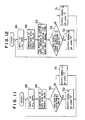
signal processor 35 under consideration is constituted by a microprocessor including adata input circuit 35A, abus 35B, a CPU (central processing unit) 35C, a RAM (random access memory) 35D, a ROM (read-only memory) 35E and adata output circuit 35F. Thedata input circuit 35 having inputs connected to n types of sensors A₁ to N₁ is connected to thebus 35B which in turn is connected to theCPU 35C, theRAM 35D, theROM 35 E and thedata output circuit 35F, respectively. TheROM 35E stores therein processing procedure illustrated in Fig. 11. TheCPU 35C executes operation in accordance with the processing procedure stored in theROM 35E. TheRAM 35D stores therein the data supplied from thedata input circuit 35A as well as the data resulting from the operation of theCPU 35C. Each of thesignal processors 1 to 4 shown in Fig. 1 may be constituted by thissignal processor 35. - Next, a processing routine for producing the trip signal in accordance with the processing procedure illustrated in Fig. 11 will be described on the assumption that the
signal processor 35 is employed as theprocessor 1 of the system shown in Fig. 1. Measurement data signals produced by the sensors A₁.. , N₁ are written in theRAM 35D by way of thedata input circuit 35A. TheCPU 35C reads the processing procedure illustrated in Fig. 11 from theROM 35E. In astep 48 of the processing procedure, theCPU 35C reads the measurement data from theRAM 35D. Each measurement data as read into theCPU 35C is compared with a predetermined value (a preset scram value) at astep 49. Subsequently, decision is made at astep 50 as to whether there is the measurement data which exceeds the predetermined value. If the result of comparison is negative (NO), theCPU 35C produces the signal a of logic "1" at astep 51. Otherwise, theCPU 35C produces the signal a of astep 52. The value of the signal a thus produced is once stored in theRAM 35D and thereafter transferred to theswitching circuit 19A through thedata output circuit 35F. The processing at thesteps 48 to 50 and 51 or step 48 to 50 and 52 is repeated for each measurement data as inputted. When the signal processor is employed as thesignal processors steps - Another example of the processing procedure is illustrated in Fig. 12 which differs from the one shown in Fig. 11 in that the
step 54 is replaced by thestep 50 and that thestep 53 is newly provided. This processing procedure can be advantageously applied to the case where the measurement data obtained from the sensors A₁ to A₄, ..., N₁ to N₄ (i e. all the different types of measured status quantity signals) are inputted to one signal processor each in quadruplet. Thesignal processor 35 to which this processing procedure can be applied corresponds to the signal processor 1A (or 2A, 3A or 4A) of the system shown in Fig. 6. The following description is directed to the portions of the processing procedure which differ from those illustrated in Fig. 11. At astep 53, it is decided whether at least two of the four same type measurement data undergone the comparison at thestep 49 exceeds the predetermined value (decision based on the 2-out-of-4 voting logic) and produces the trip signal (of logic "0") when the predetermined value is exceeded. More specifically, at thestep 53, decision is made for every measurement data of n different types as to whether at least two same type measurement data exceeds the predetermined value. Subsequently, execution proceeds to astep 54 where decision is made as to whether at least one of the results of decision made for the different type measurement data on the basis of the 2-out-of-4 logic is logic "0" or not. When the decision made at thestep 54 results in "NO", the processing indicated at astep 51 is executed. Otherwise, the processing indicated at astep 52 is performed. - The nuclear reactor safety control safeguard system differing from the one shown in Fig. 1 in that the signal processors described above in conjunction with Figs. 10 and 12 are employed can enjoy advantageous effects similar to those attainable with the system shown Fig. 1. Besides, because each processor is constituted by microprocessor, the system can be realized in a compact structure, to further advantage. The embodiment described above in conjunction with Fig. 12 can assure substantially same effects as those attainable with the system shown in Fig. 6.
- As will now be understood, the structure of switch apparatus can be simplified while the reliability of the safety control safeguard system can be significantly improved according to the present invention.
Claims (20)
sensors (A₁, A₂, A₃, A₄) installed in a quadruple array;
first, second, third and fourth signal processing channels (25A, 25B, 25C, 25D) provided in parallel and each including signal processing means for receiving output signals from said sensors for producing a trip signal;
a pair of actuating means (16, 17) operable independent of each other;
an apparatus (18, 19) controlled through operation of said actuating means; and
switch means (5A, 5B) operatively connected to said first, second, third and fourth processing channels for activating said two actuating means in response to application of trip signals produced by at least two of said signal processing channels.
decision means for receiving status quantity signals produced by said sensors to make dicision as to whether said status quantity signals exceed a predetermined value;
2-out-of-4 logic means provided in a number n equal to that of said sensors for producing the status quantity signals of different types and each receiving a first output signal from said decision means which corresponds to four same type status quantity signals; and
1-out-of-n logic means having inputs supplied with second output signals first all of said 2-out-of-4 logic means to produce said trip signal when at least one of said second output signal exceeds the predetermined value.
sensors (A₁, A₂, A₃, A₄) installed in a quadruple array;
first, second, third and fourth signal processing channels (25A, 25B, 25C, 25D) provided in parallel and each including signal processing means for receiving output signals from said sensors for producing a trip signal;
a pair of actuating means (16, 17) operable independent of each other;
an apparatus (18, 19) to be controlled through operation of said actuating means; and
switch means (5A, 5B) operatively connected to said first, second, third and fourth processing channels for receiving said trip signal produced by said signal processing channels and constituting in cooperation with said two actuating means a 2-out-of-4 logic circuit.
decision means for receiving status quantity signals produced by said sensors to make decision as to whether said status quantity signals exceed a predetermined value;
2-out-of-4 logic means provided in a number n equal to that of said sensors for producing the status quantity signals of different types and each receiving a first output signal from said decision means which corresponds to four same type status quantity signals; and
1-out-of-n logic means having input supplied with second output signals from all of said 2-out-of-4 logic means to produce said trip signal when at least one of said second output signal exceeds the predetermined value.
sensors (A₁, A₂, A₃, A₄) installed in a quadruple array;
first, second, third and fourth signal processing channels (25A, 25B, 25C, 25D) provided in parallel and each including a microprocessor for receiving output signals from said sensors for producing a trip signal;
a pair of actuating means (16, 17) operable independent of each other;
an apparatus (18, 19) to be controlled through operation of said actuating means; and
switch means (5A, 5B) operatively connected to said first, second, third and fourth processing channels for activating said two actuating means in response to application of trip signals produced by at least two of said signal processing channels.
sensor (A₁, A₂, A₃, A₄) installed in a quadruple array;
first, second, third and fourth signal processing channels (25A, 25B, 25C, 25D) provided in parallel and each including a microprocessor for receiving output signals from said sensor for producing a trip signal;
a pair of actuating means (16, 17) operable independent of each other;
an apparatus (18, 19) to be controlled through operation of said actuating means; and
switch means (5A, 5B) operatively connected to said first, second, third and fourth processing channels for receiving the trip signals produced by at least two of said signal processing channels, and constituting through cooperation with said two actuating means a 2-out-of-4 logic circuit.
sensors (A₁, A₂, A₃, A₄) installed in a quadruple array;
first, second, third and fourth signal processing channels (25A, 25B, 25C, 25D) provided in parallel and each including signal processing means for receiving output signals from said sensors for producing a trip signal;
first and second actuating means (16, 17) operable independent of each other;
an apparatus (18, 19) to be controlled through operation of said actuating means;
first switch means (5A) operatively connected to said first, second, third and fourth processing channels for activating said first actuating means in response to application of a trip signal produced by said signal processing channels; and
second switch means (5B) operatively connected to said first, second, third and fourth processing channels for activating said second actuating means in response to application of a trip signal produced by said signal processing channels,
wherein said first and second switch means and said first and second actuating means constitute a 2-out-of-4 logic circuit.
decision means for receiving status quantity signals produced by said sensors to make decision as to whether said status quantity signals exceed a predetermined value;
2-out-of-4 logic means provided in a number n equal to that of said sensors for producing the status quantity signals of different types and each receiving a first output signal from said decision means which corresponds to four same type status quantity signals; and
1-out-of-n logic means having inputs supplied with second output signals from all of said 2-out-of-4 logic means to produce said trip signal when at least one of said second output signals exceeds the predetermined value.
sensors (A₁, A₂, A₃, A₄) installed in a quadruple array;
first, second, third and fourth signal processing channels (25A, 25B, 25C, 25D) provided in parallel and each including signal processing means receiving output signals from said sensors for producing a trip signal;
first switch means (5A) including a circuit composed of a first switch element, a second switch element and a parallel connection of third and fourth switch elements which are connected in series to one another;
second switch means (5B) including a circuit composed of a fifth switch element, a sixth switch element and a parallel connection of seventh and eighth switch elements which are connected in series to one another;
first actuating means (16) connected to the output end of said first switch means;
second actuating means (17) connected to the output end of said second switch means and operable independent of said first actuating means;
an apparatus (18, 19) to be controlled through operation of said first and second actuating means;
wherein trip signals outputted from two of said signal processing channels are effective to open either one of said first and second switch elements, respectively, while trip signals outputted from the remaining two signal processing channels are effective to open either one of said fifth and sixth switch elements, respectively, said trip signals outputted from the first mentioned signal processing channels being further effective to open either one of said seventh and eighth switch elements, respectively, while the trip signals outputted from said remaining two signal processing channels are effective to open either one of said third and fourth switch elements, respectively.
sensors (A₁, A₂, A₃, A₄) installed in a quadruple array;
first, second, third and fourth signal processing channels (25A, 25B, 25C, 25D) provided in parallel and each including signal processing means for receiving output signals from said sensors for producing a trip signal and switching means connected to said signal processing means;
a pair of actuating means (16, 17) operable independent of each other;
an apparatus (18, 19) to be controlled through operation of said actuating means; and
switch means (5A, 5B) operatively connected to said first, second, third and fourth processing channels for activating said two actuating means in response to application of trip signals produced by at least two of said signal processing channels.
first, second, third and fourth signal processing channels (25A, 25B, 25C, 25D) provided in parallel and each including signal processing means for receiving output signals from said sensors for producing a trip signal and switching means connected to said signal processing means;
a pair of actuating means (16, 17) operable independent of each other;
an apparatus (18, 19) to be controlled through operation of said actuating means; and
switch means (5A, 5B) operatively connected to said first, second, third and fourth processing channels for receiving said trip signal produced by said signal processing channels and constituting in cooperation with said two actuating means a 2-out-of-4 logic circuit.
sensors (A₁, A₂, A₃, A₄) installed in a quadruple array;
first, second, third and fourth signal processing channels (25A, 25B, 25C, 25D) provided in parallel, each of said signal processing channels including signal processing means for receiving output signals from said sensors for producing a trip signal, switching means connected to said signal processing means and diagnosis means for deciding presence or absence of abnormality in said signal processing means to thereby output an operation command to said switching means for causing said signal processing means to be disconnected when abnormality is present;
a pair of actuating means (16, 17) operable independent of each other;
an apparatus (18, 19) to be controlled through operation of said actuating means; and
switch means (5A, 5B) operatively connected to said first, second, third and fourth processing channels for activating said two actuating means in response to application of trip signals produced by at least two of said signal processing channels.
sensors (A₁, A₂, A₃, A₄) installed in a quadruple array;
first, second, third and fourth signal processing channels (25A, 25B, 25C, 25D) provided in parallel, each of said signal processing channels including signal processing means for receiving output signals from said sensors for producing a trip signal, switching means connected to said signal processing means and diagnosis means for deciding presence or absence of abnormality in said signal processing means to output an operation command to said switching means for causing said signal processing means to be disconnected when abnormality is present;
a pair of actuating means (16, 17) operable independent of each other;
an apparatus (18, 19) to be controlled through operation of said actuating means; and
switch means (5A, 5B) operatively connected to said first, second, third and fourth processing channels for receiving said trip signal produced by said signal processing channels and constituting in cooperation with said two actuating means a 2-out-of-4 logic circuit.
a plural types of sensors (A₁, A₂, A₃, A₄), each type of sensors being installed in a quadruple array;
first, second, third and fourth signal processing channels (25A, 25B, 25C, 25D) provided in parallel and each including a plurality of first microprocessors for receiving output signals from the associated sensors, respectively, for producing trip signals and a second microprocessor including a majority logic circuit receiving the output signals of said first microprocessors to output a trip signal;
a pair of actuating means (16, 17) operable independent of each other;
an apparatus (18, 19) to be controlled through operation of said actuating means; and
switch means (5A, 5B) operatively connected to said first, second, third and fourth processing channels for receiving said trip signal produced by said signal processing channels and constituting in cooperation with said two actuating means a 2-out-of-4 logic circuit.
Applications Claiming Priority (3)
| Application Number | Priority Date | Filing Date | Title |
|---|---|---|---|
| JP15607186 | 1986-07-04 | ||
| JP62004834A JPH0795241B2 (en) | 1986-07-04 | 1987-01-14 | Reactor safety protection device |
| JP4834/87 | 1987-01-14 |
Publications (3)
| Publication Number | Publication Date |
|---|---|
| EP0275362A2 true EP0275362A2 (en) | 1988-07-27 |
| EP0275362A3 EP0275362A3 (en) | 1989-08-30 |
| EP0275362B1 EP0275362B1 (en) | 1994-07-13 |
Family
ID=26338677
Family Applications (1)
| Application Number | Title | Priority Date | Filing Date |
|---|---|---|---|
| EP87113354A Expired - Lifetime EP0275362B1 (en) | 1986-07-04 | 1987-09-11 | Safety control system |
Country Status (2)
| Country | Link |
|---|---|
| US (1) | US4843537A (en) |
| EP (1) | EP0275362B1 (en) |
Cited By (4)
| Publication number | Priority date | Publication date | Assignee | Title |
|---|---|---|---|---|
| EP0458639A2 (en) * | 1990-05-24 | 1991-11-27 | Hitachi, Ltd. | Servo valve control method and apparatus |
| WO1993020488A2 (en) * | 1992-03-31 | 1993-10-14 | The Dow Chemical Company | Process control interface system having triply redundant remote field units |
| WO2001041153A1 (en) * | 1999-12-06 | 2001-06-07 | Westinghouse Electric Company Llc | Energize to actuate engineered safety features actuation system and testing method therefor |
| EP3236552A4 (en) * | 2014-12-15 | 2018-09-19 | YPP Co. Ltd. | Triple redundant digital protective relay and operating method therefor |
Families Citing this family (13)
| Publication number | Priority date | Publication date | Assignee | Title |
|---|---|---|---|---|
| JPH0731537B2 (en) * | 1987-09-11 | 1995-04-10 | 株式会社日立製作所 | Multiplex controller |
| FR2626403B1 (en) * | 1988-01-27 | 1990-05-11 | Framatome Sa | PROTECTION SYSTEM FOR A NUCLEAR REACTOR IN THE EVENT OF A FALL OF AN ANTIREACTIVE ELEMENT |
| US5287264A (en) * | 1988-08-05 | 1994-02-15 | Hitachi, Ltd. | Multicontroller apparatus, multicontroller system, nuclear reactor protection system, inverter control system and diagnostic device |
| FR2715738B1 (en) * | 1994-01-31 | 1996-04-12 | Sextant Avionique | Composite safety switch. |
| JP3848074B2 (en) * | 2000-10-31 | 2006-11-22 | 株式会社日立製作所 | Reactor manual operation device |
| US6701258B2 (en) * | 2002-05-13 | 2004-03-02 | Entek Ird International Corporation | Modular monitoring and protection system with distributed voting logic |
| US6798859B1 (en) * | 2003-08-18 | 2004-09-28 | General Electric Company | Branch amplifier card |
| US7177383B2 (en) * | 2004-02-02 | 2007-02-13 | James Hardy | Method and system for safety regulation in nuclear power regulating systems |
| KR100848881B1 (en) | 2006-08-07 | 2008-07-29 | 삼창기업 주식회사 | Digital Security System for Nuclear Power Plant |
| KR100980043B1 (en) | 2008-10-22 | 2010-09-06 | 한국전력기술 주식회사 | System and method of protecting a power plant using FPGA |
| JP5422448B2 (en) | 2010-03-10 | 2014-02-19 | 株式会社東芝 | Control device |
| JP5701033B2 (en) * | 2010-12-09 | 2015-04-15 | 三菱重工業株式会社 | Reactor shutdown device |
| US9997265B2 (en) * | 2015-03-27 | 2018-06-12 | Mitsubishi Electric Power Products, Inc. | Safety system for a nuclear power plant and method for operating the same |
Citations (4)
| Publication number | Priority date | Publication date | Assignee | Title |
|---|---|---|---|---|
| GB2142206A (en) * | 1983-06-24 | 1985-01-09 | Atomic Energy Authority Uk | Monitoring system |
| EP0180085A2 (en) * | 1984-10-31 | 1986-05-07 | Westinghouse Electric Corporation | Distributed microprocessor based sensor signal processing system for a complex process |
| EP0202052A2 (en) * | 1985-05-09 | 1986-11-20 | Westinghouse Electric Corporation | Auxiliary reactor protection system and method |
| EP0221775A1 (en) * | 1985-10-31 | 1987-05-13 | Westinghouse Electric Corporation | Testable voted logic power circuit and method of testing the same |
Family Cites Families (6)
| Publication number | Priority date | Publication date | Assignee | Title |
|---|---|---|---|---|
| US4434132A (en) * | 1981-04-09 | 1984-02-28 | Westinghouse Electric Corp. | Power supply with nuclear reactor |
| US4697093A (en) * | 1985-01-23 | 1987-09-29 | Westinghouse Electric Corp. | Testable, fault-tolerant power interface circuit for controlling plant process equipment |
| US4687623A (en) * | 1985-10-31 | 1987-08-18 | Westinghouse Electric Corp. | Self-compensating voted logic power interface with tester |
| US4664870A (en) * | 1985-10-31 | 1987-05-12 | Westinghouse Electric Corp. | Testable voted logic power interface |
| US4683105A (en) * | 1985-10-31 | 1987-07-28 | Westinghouse Electric Corp. | Testable, fault-tolerant power interface circuit for normally de-energized loads |
| US4696785A (en) * | 1985-10-31 | 1987-09-29 | Westinghouse Electric Corp. | Testable voted logic power circuit and method of testing the same |
-
1987
- 1987-07-02 US US07/069,046 patent/US4843537A/en not_active Expired - Lifetime
- 1987-09-11 EP EP87113354A patent/EP0275362B1/en not_active Expired - Lifetime
Patent Citations (4)
| Publication number | Priority date | Publication date | Assignee | Title |
|---|---|---|---|---|
| GB2142206A (en) * | 1983-06-24 | 1985-01-09 | Atomic Energy Authority Uk | Monitoring system |
| EP0180085A2 (en) * | 1984-10-31 | 1986-05-07 | Westinghouse Electric Corporation | Distributed microprocessor based sensor signal processing system for a complex process |
| EP0202052A2 (en) * | 1985-05-09 | 1986-11-20 | Westinghouse Electric Corporation | Auxiliary reactor protection system and method |
| EP0221775A1 (en) * | 1985-10-31 | 1987-05-13 | Westinghouse Electric Corporation | Testable voted logic power circuit and method of testing the same |
Non-Patent Citations (1)
| Title |
|---|
| PROCEEDINGS IECON '84, 1984 INTERNATIONAL CONFERENCE ON INDUSTRIAL ELECTRONICS, CONTROL AND INSTRUMENTATION, Tokyo, 22nd-26th October 1984, vol. 2, pages 1181-1184, IEEE, New York, US; K. ASAMI et al.: "Super-high reliability fault tolerant system NURECS-3000" * |
Cited By (10)
| Publication number | Priority date | Publication date | Assignee | Title |
|---|---|---|---|---|
| EP0458639A2 (en) * | 1990-05-24 | 1991-11-27 | Hitachi, Ltd. | Servo valve control method and apparatus |
| EP0458639A3 (en) * | 1990-05-24 | 1993-06-02 | Hitachi, Ltd. | Servo valve control method and apparatus |
| WO1993020488A2 (en) * | 1992-03-31 | 1993-10-14 | The Dow Chemical Company | Process control interface system having triply redundant remote field units |
| WO1993020488A3 (en) * | 1992-03-31 | 1994-03-31 | Dow Chemical Co | Process control interface system having triply redundant remote field units |
| EP0869415A2 (en) * | 1992-03-31 | 1998-10-07 | The Dow Chemical Company | Process control interface system having triply redundant remote field units |
| US5970226A (en) * | 1992-03-31 | 1999-10-19 | The Dow Chemical Company | Method of non-intrusive testing for a process control interface system having triply redundant remote field units |
| EP0869415A3 (en) * | 1992-03-31 | 1999-12-15 | The Dow Chemical Company | Process control interface system having triply redundant remote field units |
| WO2001041153A1 (en) * | 1999-12-06 | 2001-06-07 | Westinghouse Electric Company Llc | Energize to actuate engineered safety features actuation system and testing method therefor |
| EP3236552A4 (en) * | 2014-12-15 | 2018-09-19 | YPP Co. Ltd. | Triple redundant digital protective relay and operating method therefor |
| US10158220B2 (en) | 2014-12-15 | 2018-12-18 | Ypp Co., Ltd. | Triple redundant digital protective relay and operating method therefor |
Also Published As
| Publication number | Publication date |
|---|---|
| EP0275362A3 (en) | 1989-08-30 |
| EP0275362B1 (en) | 1994-07-13 |
| US4843537A (en) | 1989-06-27 |
Similar Documents
| Publication | Publication Date | Title |
|---|---|---|
| EP0275362B1 (en) | Safety control system | |
| EP1010044B1 (en) | Safety or protection system employing reflective memory and/or diverse processors and communications | |
| US6532550B1 (en) | Process protection system | |
| US6842669B2 (en) | Component interface module | |
| CN108022662B (en) | Digital protection system of nuclear power station | |
| US5287264A (en) | Multicontroller apparatus, multicontroller system, nuclear reactor protection system, inverter control system and diagnostic device | |
| KR20180125336A (en) | Nuclear power plant digital protection system | |
| CN111681792B (en) | ATWT control device and nuclear power equipment | |
| JP2501178B2 (en) | Reactor safety protection device | |
| EP1433185B1 (en) | Interface module for a controlled component | |
| KR950008093B1 (en) | Control system | |
| US5196158A (en) | Electrical safety system | |
| CN212716781U (en) | Steam turbine electron hypervelocity interdiction system with high fault-tolerant characteristic | |
| JPH07134601A (en) | Double bus control method | |
| KR19980024802A (en) | Pump selection logic circuit | |
| JP2907930B2 (en) | Nuclear power plant safety protection equipment | |
| CN1145975C (en) | Pump selection logic | |
| JP3099600B2 (en) | Selection control rod controller | |
| JP2988476B2 (en) | Reactor protection device | |
| von Haebler et al. | The PWR Protection System-Present and Future | |
| CA2304438C (en) | Safety or protection system employing reflective memory and/or diverse processors and communications | |
| JPS62165183A (en) | Protective device for nuclear reactor | |
| JPS63234193A (en) | Safety protective device for nuclear reactor | |
| JPH0542687B2 (en) | ||
| JPS63135669A (en) | Relief valve |
Legal Events
| Date | Code | Title | Description |
|---|---|---|---|
| PUAI | Public reference made under article 153(3) epc to a published international application that has entered the european phase |
Free format text: ORIGINAL CODE: 0009012 |
|
| AK | Designated contracting states |
Kind code of ref document: A2 Designated state(s): DE FR GB |
|
| PUAL | Search report despatched |
Free format text: ORIGINAL CODE: 0009013 |
|
| AK | Designated contracting states |
Kind code of ref document: A3 Designated state(s): DE FR GB |
|
| 17P | Request for examination filed |
Effective date: 19891128 |
|
| 17Q | First examination report despatched |
Effective date: 19911025 |
|
| GRAA | (expected) grant |
Free format text: ORIGINAL CODE: 0009210 |
|
| AK | Designated contracting states |
Kind code of ref document: B1 Designated state(s): DE FR GB |
|
| REF | Corresponds to: |
Ref document number: 3750218 Country of ref document: DE Date of ref document: 19940818 |
|
| ET | Fr: translation filed | ||
| PLBE | No opposition filed within time limit |
Free format text: ORIGINAL CODE: 0009261 |
|
| STAA | Information on the status of an ep patent application or granted ep patent |
Free format text: STATUS: NO OPPOSITION FILED WITHIN TIME LIMIT |
|
| 26N | No opposition filed | ||
| REG | Reference to a national code |
Ref country code: GB Ref legal event code: IF02 |
|
| PGFP | Annual fee paid to national office [announced via postgrant information from national office to epo] |
Ref country code: FR Payment date: 20060814 Year of fee payment: 20 |
|
| PGFP | Annual fee paid to national office [announced via postgrant information from national office to epo] |
Ref country code: GB Payment date: 20060816 Year of fee payment: 20 |
|
| PGFP | Annual fee paid to national office [announced via postgrant information from national office to epo] |
Ref country code: DE Payment date: 20060828 Year of fee payment: 20 |
|
| REG | Reference to a national code |
Ref country code: GB Ref legal event code: PE20 |
|
| PG25 | Lapsed in a contracting state [announced via postgrant information from national office to epo] |
Ref country code: GB Free format text: LAPSE BECAUSE OF EXPIRATION OF PROTECTION Effective date: 20070910 |