EP0272491A2 - In einem tiefen Graben formierte Isolation mit Kontakt an der Oberfläche des Substrates - Google Patents
In einem tiefen Graben formierte Isolation mit Kontakt an der Oberfläche des Substrates Download PDFInfo
- Publication number
- EP0272491A2 EP0272491A2 EP87117479A EP87117479A EP0272491A2 EP 0272491 A2 EP0272491 A2 EP 0272491A2 EP 87117479 A EP87117479 A EP 87117479A EP 87117479 A EP87117479 A EP 87117479A EP 0272491 A2 EP0272491 A2 EP 0272491A2
- Authority
- EP
- European Patent Office
- Prior art keywords
- trench
- semiconductor
- further including
- layer
- substrate
- Prior art date
- Legal status (The legal status is an assumption and is not a legal conclusion. Google has not performed a legal analysis and makes no representation as to the accuracy of the status listed.)
- Granted
Links
Images

Classifications
-
- H—ELECTRICITY
- H01—ELECTRIC ELEMENTS
- H01L—SEMICONDUCTOR DEVICES NOT COVERED BY CLASS H10
- H01L21/00—Processes or apparatus adapted for the manufacture or treatment of semiconductor or solid state devices or of parts thereof
- H01L21/70—Manufacture or treatment of devices consisting of a plurality of solid state components formed in or on a common substrate or of parts thereof; Manufacture of integrated circuit devices or of parts thereof
- H01L21/71—Manufacture of specific parts of devices defined in group H01L21/70
- H01L21/76—Making of isolation regions between components
-
- H—ELECTRICITY
- H01—ELECTRIC ELEMENTS
- H01L—SEMICONDUCTOR DEVICES NOT COVERED BY CLASS H10
- H01L21/00—Processes or apparatus adapted for the manufacture or treatment of semiconductor or solid state devices or of parts thereof
- H01L21/70—Manufacture or treatment of devices consisting of a plurality of solid state components formed in or on a common substrate or of parts thereof; Manufacture of integrated circuit devices or of parts thereof
- H01L21/71—Manufacture of specific parts of devices defined in group H01L21/70
- H01L21/74—Making of localized buried regions, e.g. buried collector layers, internal connections substrate contacts
- H01L21/743—Making of internal connections, substrate contacts
-
- H—ELECTRICITY
- H01—ELECTRIC ELEMENTS
- H01L—SEMICONDUCTOR DEVICES NOT COVERED BY CLASS H10
- H01L21/00—Processes or apparatus adapted for the manufacture or treatment of semiconductor or solid state devices or of parts thereof
- H01L21/70—Manufacture or treatment of devices consisting of a plurality of solid state components formed in or on a common substrate or of parts thereof; Manufacture of integrated circuit devices or of parts thereof
- H01L21/71—Manufacture of specific parts of devices defined in group H01L21/70
- H01L21/76—Making of isolation regions between components
- H01L21/763—Polycrystalline semiconductor regions
Definitions
- the present invention relates in general to semiconductor structures and methods of fabrication thereof, and more particularly relates to methods and structures for providing lateral isolation between semiconductor circuits formed on a substrate.
- the scaling of integrated circuits to increase the packing density is accomplished by reducing the lateral dimensions of the transistor features. Generally, the various photolithographic masks are reduced in size so that the resulting circuits are also reduced in size.
- the scaling of P-channel (PMOS) insulated gate field effect transistors and N-channel (NMOS) transistors can be accomplished without substantial deterioration in performance, as the features of the transistors are laterally oriented at the face of the semiconductor body.
- bipolar transistors can also be scaled to increase packing density, the lateral size of the device cannot be scaled as easily, as this family of devices is not a lateral-operating device, but rather depends upon the particular vertical spacing of semiconductor layers orthogonal to the face of the semiconductor body.
- a major concern with scaling integrated circuits is the electrical isolation which must be maintained between the circuits. In other words, and unless otherwise desired, the electrical operation of one circuit must be independent of that of an adjacent circuit.
- One approach conventionally utilized for isolating circuits, especially of the bipolar type is to form an N-type buried layer on a P-type substrate, and deposit a P-type epitaxial layer thereover. An N-well is formed in the epitaxial layer down and in contact with the buried layer. The base and emitter features of the bipolar transistor, as well as the collector contact, are formed in the N-well. The epitaxial layer surrounding the N-well is effective to isolate the bipolar transistor from adjacent circuits. This isolation technique is commonly referred to as the collector diffused isolation technology.
- the standard buried collector technique is similar to the collector diffused isolation technique, but instead of forming a semiconductor well in the epitaxial layer, an annular P-type isolation ring is formed around an N epitaxial layer overlying the buried collector, thereby isolating the epitaxial well from adjacent circuits.
- the base, emitter and collector contact semiconductor regions are formed in the isolated epitaxial region.
- Still another isolation technique involves the formation on an annular ring of a P-type semiconductor material surrounding and spaced apart from a buried collector. An epitaxial layer is deposited thereover, and a second P-type annular ring is formed in the epitaxial layer, overlying the bottom isolation ring. A thermal diffusing of the upper and bottom P-type isolation rings causes such rings to be joined, thereby encircling a portion of the epitaxial region and isolating it from adjacent circuits.
- junction isolation techniques The disadvantage with such previously developed junction isolation techniques is that a substantial amount of lateral wafer area is required to form the isolation structures themselves.
- the wafer area problem encountered in utilizing junction-type isolation is further aggravated in fabricating high voltage bipolar transistors where the epitaxial layer is required to be relatively thick.
- a diffused isolation region which extends from the face of the semiconductor body to the substrate also diffuses in the lateral direction to such an extent that appreciable wafer area is used.
- a certain amount of "wasted" lateral area must be reserved between the isolation diffusions of adjacent circuits to prevent breakdown or "punch-through" between adjacent circuits.
- the wafer area required by the isolation diffusions and the wasted space may account for more than half the entire area of the circuit.
- Another isolation technology conventionally employed in fabricating semiconductor circuits comprises an oxide isolation formed between circuits to be isolated.
- One technique utilizing oxide isolation includes masking circuit areas and selectively oxidizing through an epitaxial layer into an underlying substrate. Hence, adjacent circuits are electrically isolated by the silicon oxide. This technique is limited to the isolation of circuits formed in thin epitaxial layers. An uneven topographical surface may result when this method is attempted in conjunction with thicker epitaxial layers. In forming the isolation oxide with this technique, the oxide experiences a lateral spreading which encroaches on active circuit areas.
- Another oxide isolation technique involves the formation of a deep trench anisotropically etched into the semiconductor material, and sloped etched at the upper trench corners to reduce the subsequent formation of crystal faults due to high temperature oxidation.
- a thin layer of silicon oxide is then formed on the trench sidewalls.
- a layer of silicon nitride is deposited on the trench sidewalls, and the trench is filled with polycrystalline silicon. Planarization of the wafer surface is required to form a topography suitable for subsequent masking, patterning and fabrication steps.
- This technique is disclosed in an article titled "Isolation Technique for High Speed Bipolar VLSI's", pp. 62-65, Vol. 82 IEEE Journal, 1982.
- a major drawback associated with forming deep trenches is the damage to the silicon semiconductor material in regions adjacent the trench caused by subsequent annealing or heat treatment of the wafer, such as subsequent oxidation steps.
- the corners of the trench are known to be the mechanism for generating crystallographic dislocations and faults which extend substantial distances from the trench.
- Semiconductor circuits formed in the silicon material having these faults generally exhibit leaky PN junctions which severely deteriorate the performance of the circuit.
- oxide isolation in general is that there is no longer an electrically active medium from the surface to the underlying substrate. This shortcoming is often circumvented by providing a substrate contact on the backside thereof. Backside processing of the wafer requires special packaging techniques, including alloy mounting of a header to the chip.
- the disclosed isolation technique and structure reduces or eliminates the disadvantages and shortcomings associated with the prior art techniques.
- a trench of adequate depth is formed through the active semiconductor material, down to the substrate, and oxidized to form a thin layer of isolating material on the sidewalls thereof.
- An oxidation barrier such as a nitride layer, is formed over the surface of the wafer, including the sidewalls and the bottom of the trench.
- the wafer is then subjected to a reactive ion etch (RIE) in which the top surface nitride and silicon oxide are removed, as well as the nitride and silicon oxide at the bottom of the trench.
- RIE reactive ion etch
- the resulting wafer includes a surface layer of silicon nitride which is continuous with the nitride on the trench sidewalls.
- the bottom of the trench comprises an exposed surface of the substrate.
- the nitride mask formed around the top corners of the trench provides an oxidation barrier mask to prevent silicon crystallographic dislocations and faults which could otherwise result during subsequent and necessary oxidation processing of the wafer.
- a conformal layer of highly doped polycrystalline silicon (polysilicon) is then deposited over the surface of the wafer with a thickness sufficient to completely fill the trench.
- the conductive polysilicon is in electrical contact at the bottom of the trench with the underlying substrate.
- the conformal layer of polysilicon is planarized to provide a surface suitable for subsequent circuit fabrication, which may include multiple oxidation steps.
- the technical advantage afforded this technique is that the nitride layer covering the upper trench corners avoids the bidirectional growth of the silicon causing dislocation centers in the silicon crystal lattice.
- the grounding of the substrate which is typical, provides an electrostatic shield which separates the circuits formed on each side of the trench.
- a top surface contact can be made through the conductive polysilicon of the trench, thereby providing a top surface substrate contact.
- the isolation trench includes in the face of the wafer a semiconductor region adjacent the trench, and formed of a conductivity type opposite that of the epitaxial region. The surface-oriented region provides an increased area on which a conductor can be formed to make contact with the conductive polysilicon of the narrow trench.
- the surface oriented semiconnector region and the underlying epitaxial region form a reverse-biased junction, thereby isolating the top side substrate conductor from the epitaxial region.
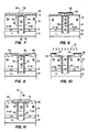
- an exemplary integrated circuit is formed using a P-type semiconductor substrate 10 as the basis thereof.
- a heavily doped buried layer 12 is formed on the substrate 10, such as by conventional ion implant and/or deposition processes.
- the thickness of the epitaxial layer may be nominally 8 microns thick, depending on the type of device desired to be formed therein.
- the buried layer 12 is shown heavily doped with an N-type impurity which is suitable for use as a buried collector in bipolar transistor circuits.
- the buried layer 12 can be formed by diffusing an N-type impurity into the P-type substrate so as to form a counter doped surface layer of N-type material.
- An additional layer 14 of semiconductor material may be deposited by an epitaxial process on the buried layer 12.
- the epitaxial layer 14 is shown having an N-type conductivity, which is suitable for use in forming NPN bipolar transistors or P-channel MOSFET transistors.
- the epitaxial layer 14 may be deposited to a thickness of 2-3 microns for low voltage bipolar transistors and MOSFET transistors, or to a greater depth for higher voltage bipolar transistors.
- FIGURE 2 illustrates the construction of the wafer after a thin silicon dioxide layer 16, a silicon nitride layer 18, and a thicker silicon dioxide layer 20 have been formed on the surface of the epitaxial layer 14.
- the silicon dioxide layer 16 is formed with a thickness of about 1,000 angstroms by the oxidation of a top surface of the epitaxial layer 14 in the presence of oxygen.
- the silicon nitride layer 18 can be deposited to a thickness of about a 1,000 angstroms by a low pressure chemical vapor deposition (LPCVD) process over the surface of the silicon dioxide 16.
- the silicon dioxide layer 16 is formed over the surface of the epitaxial layer 14 before the nitride layer 18 to prevent contact thereof to the epitaxial material 14.
- the silicon nitride layer 18 forms an oxidation barrier which prevents the top surface of the epitaxial layer 14 from being converted into silicon dioxide during subsequent oxidation process steps.
- a thick layer 20 of silicon dioxide is deposited over the silicon nitride layer 18 for use during subsequent etching to form a trench.
- the silicon dioxide may be formed to a thickness of 14,000-15,000 angstroms, by the conventional decomposition of tetraethoxysilane (TEOS).
- TEOS tetraethoxysilane
- a photoresist mask layer 22 is next spun, or otherwise deposited, over the surface of the deposited silicon dioxide 20.
- the photoresist mask layer 22 is patterned to form an opening 24 for defining the location of the trench. While the cross sectional view of FIGURE 2 illustrates a single opening, in practice, the patterned photoresist mask 22 would define the trench opening encircling an underlying epitaxial region in which it is desired to form a circuit.
- the wafer is subjected to a dry etch, such as by a reactive ion etch, to remove that portion of the silicon dioxide layers 16 and 20 and that portion of the silicon nitride layer 18 defined by the trench opening 24.
- a dry etch such as by a reactive ion etch
- the photoresist mask layer 22 is then removed.
- the reactive ion etch process is continued until a trench 26, with vertical sidewalls 28 and 30 and a bottom 32, have been formed in the underlying semiconductor layers.
- the trench width may be as small as 2-3 microns. It can be appreciated that by forming an isolation of such dimensions, a minimal amount of lateral wafer area is used for isolation purposes.
- the isolation trench area required is reduced over that used in tapering the trench corners as disclosed in the prior art. A majority of the wafer area may thus be used in fabricating the devices of circuits, thereby optimizing the use of the wafer for the circuits themselves.
- the trench 26 is formed through the epitaxial layer 14 and the heavily doped buried layer 12 down to the substrate 10. Indeed, a portion of the substrate material defines the bottom surface 32 of the trench 26.
- plural isolated semiconductor regions are formed, each of which can be used for fabricating therein independently operating circuits. It is to be noted, however, that the substrate 10 remains common to all isolated semiconductor layer.
- the independent semiconductor regions commonly termed wells or tanks, are illustrated as reference characters 34 and 36.
- the wafer is again subjected to an oxidizing environment, in which a thin silicon dioxide layer 38 and 40 is formed on the respective sidewalls 28 and 30 of the trench 26.
- the sidewall silicon dioxide 38 and 40 is formed to about the same depth as that of the surface layer 16, the two layers becoming merged or linked together at the external square trench corners 42 and 44.
- the original top surface silicon nitride layer 18 functions as an oxidation barrier, thereby preventing an additional growth of silicon dioxide on the top surface of the epitaxial regions 34 and 36.
- An additional layer 46 of silicon nitride is deposited over the surface of the wafer including the trench sidewall oxide 38 and 40, as well as on the oxidized bottom 32 of the trench 26.
- the nitride layer 46 links with the original nitride layer 18 to form plural homogeneous layers.
- the reactive ion etch process is anisotropic in nature, e.g., it is effective in unidirectionally removing material.
- material is selectively removed in the downward direction, thereby removing the laterally disposed layer of silicon nitride 46 formed on the top surface of the wafer, as well as that on the bottom 32 of the trench.
- the reactive ion etch process is continued until the oxide on the trench bottom 32 is also removed, leaving an exposed surface of the substrate 10.
- a further portion of the deposited dioxide layer 20 is removed by the dry etch.
- the removal of the deposited dioxide 20 is inconsequential, as its sole purpose is to protect the underlying nitride layer 18 from removal by the various etching steps.
- a conformal layer of P+ doped in situ polysilicon is next deposited by an LPCVD process over the surface of the wafer.
- the polysilicon is deposited to a depth sufficient to close in the sidewalls of the trench 26, and thus completely fill it.
- the doped polysilicon at the bottom of the trench 26 merges or links, both physically and electrically, with the semiconductor substrate material 10.
- the conductive polysilicon 53 filling the trench 26 is in electrical contact with the substrate 10. Due to the conformal nature of the polysilicon deposition 52, a cusp 54 is formed over the trench 26.
- the polysilicon refill 53 can be deposited as heavily doped P+ in situ material, or selectively deposited in layers with alternate diffusing or implanting with a P-type impurity to fill the trench 26. Other trench refill techniques may be utilized, including filling the trench 26 with intrinsic polysilicon, and diffusing a dopant therethrough to the underlying substrate 10.
- a photoresist material 56 is spun over the surface of the wafer.
- the photoresist material 56 is generally nonconformal, thereby leaving a flat top surface.
- a dry etch process is developed such that the etch rate of the photoresist is the same as that of the polysilicon material 52.
- the surface of the wafer is gradually and evenly removed, thus eliminating the cusp 54.
- the planarization etch is continued until the polysilicon layer 52 is removed in the areas overlying the deposited silicon dioxide layer 20.
- silicon dioxide 20 Once a large amount of silicon dioxide 20 is detected in the species of the etch system, it is known that all the polysilicon 52 has been removed. The etch process is then halted, and the only polysilicon which remains is that which exists in the trench 26. The remaining silicon dioxide 20 can be removed by other conventional etching processes.
- the wafer is subjected to an oxidizing environment in which a thin dioxide cap 58 is formed on top of the trench polysilicon 53. Because the remaining surface areas of the wafer are covered by the original nitride layer 18, further silicon dioxide growth does not occur elsewhere.
- the cap dioxide 58 is grown to about the same depth as that of the dioxide layer 16.
- An additional layer 60 of silicon nitride is formed over the surface of the wafer, linking with that of the original nitride layer 18.
- the wafer is then ready for subsequent processing to fabricate circuits in the epitaxial regions 34 and 36.
- subsequent wafer processing including high temperature oxidation steps can be performed without concern of silicon crystal dislocations forming at the external square trench corners 42 and 44.
- the conductive polysilicon 53 of the trench is also at a ground potential, and thereby provides an electrostatic shield between epitaxial regions 34 and 36. This is important in reducing the potential electrical coupling between such regions 34 and 36 due to a parasitic FET transistor, wherein a nonconductive trench refill could function as the gate insulator of the parasitic transistor.
- a topside substrate contact can be made employing the conductive material 53 of the trench refill.
- the topside contact requires no additional mask steps, but can be formed by the same steps used in fabricating the remainder of the integrated circuit.
- a photoresist mask layer 62 can be deposited on the wafer over the area defining a contact to the trench refill 53.
- the resist material 62 is patterned, as shown in FIGURE 8.
- the patterned photoresist 62 is patterned to cover underlying semiconductor areas in the respective epitaxial regions 34 and 36 for providing an expanded lateral contact area for a topside substrate contact.
- the portion of the original silicon dioxide layer 16 exposed by the mask 62 is removed by an etch process.
- the photoresist 62 is removed.
- the nitride pad 60 generally overlying the trench area provides an oxidation mask so that silicon oxide does not grow in the area covered by the patterned nitride.
- the wafer is next subjected to an oxidizing environment in which a thick field oxide 64 and 66 is grown in the areas not covered by the nitride oxidation barrier 60. This step is depicted in FIGURE 9.
- the field oxide 64 and 66 becomes homogenous with the oxide layer 16.
- the wafer is then etched by suitable processes to remove the nitride oxidation mask 60 and the thin silicon oxide 58 covering the trench refill 53. As a result, the trench refill is exposed, as are surface areas of the epitaxial regions 34 and 36 adjacent the trench.
- an additional photoresist 67 is shown spun over the wafer and patterned to open the trench area as shown.
- Heavily doped P-type semiconductor areas 68 and 70 are formed in the faces of the respective epitaxial regions 34 and 36 by an ion implantation 72.
- the trench refill 53 is unaffected by the implantation as it is already heavily doped with a P-type impurity. Boron, or other similiar impurities, may be used to form the implanted P-type regions 68 and 70.
- the photoresist mask 67 functions as a barrier to prevent the implantation of the P-type impurity in other areas of the wafer.
- the photoresist 67 is removed after the implant, and then the ions are activated by annealing the wafer. While ion implantation is preferable in forming the lateral conductive areas 68 and 70, a diffusion process may be employed in lieu thereof.
- the topside substrate is metallized along with the conventional metallization of the wafer circuits.
- an opening is formed in the area above the trench refill 53 and the semiconductor regions 68 and 70.
- a layer of conductive material or metal is formed over the surface of the wafer, masked and patterned (not shown) to form the contact electrode 74 over the conductive trench refill 53.
- the additonal lateral conductive areas 68 and 70 allow for a certain amount of misallignment of the contact electrode 74 while yet enabling it to make contact with the narrow trench refill 53.
- the contact electrode 74 can then be grounded 76 to thereby provide a ground potential to the substrate 10 through the conductive polysilicon refill 53 of the trench.
- lateral areas 68 and 70 being of the P-type conductivity, a reverse-biased junction is formed between such areas and the corresponding epitaxial regions 34 and 36, thereby maintaining the contact electrode 78 electrically isolated from the active semiconductor regions 34 and 36.
- the topside substrate contact of FIGURE 11 is preferrably formed as the last step in the wafer fabrication process, using the same process masks and metallization steps as the other circuits of the integrated circuit. Since the metallization steps are conducted at temperatures considerably lower than the silicon oxidation steps, the risk of forming crystal faults is reduced.
- One technical advantage of the trench structure arises from the oxidation barrier which protects the adjacent semiconductor regions from crystal faults and dislocations caused by high temperature oxidizing processes.
- Another technical advantage of the invention is the conductive refill of the trench which is in electrical contact with a substrate.
- the conductive trench refill functions as an electrostatic shield between adjacent semiconductor regions, thereby reducing electrical interference and parasitic transistor action therebetween.
- An additional technical advantage of the invention associated with the conductive refill of the trench is the feature which, permits topside connections to the wafer substrate.
Landscapes
- Engineering & Computer Science (AREA)
- Physics & Mathematics (AREA)
- Condensed Matter Physics & Semiconductors (AREA)
- General Physics & Mathematics (AREA)
- Manufacturing & Machinery (AREA)
- Computer Hardware Design (AREA)
- Microelectronics & Electronic Packaging (AREA)
- Power Engineering (AREA)
- Chemical & Material Sciences (AREA)
- Crystallography & Structural Chemistry (AREA)
- Element Separation (AREA)
- Semiconductor Integrated Circuits (AREA)
Applications Claiming Priority (2)
| Application Number | Priority Date | Filing Date | Title |
|---|---|---|---|
| US94574286A | 1986-12-22 | 1986-12-22 | |
| US945742 | 1986-12-22 |
Publications (3)
| Publication Number | Publication Date |
|---|---|
| EP0272491A2 true EP0272491A2 (de) | 1988-06-29 |
| EP0272491A3 EP0272491A3 (de) | 1989-03-15 |
| EP0272491B1 EP0272491B1 (de) | 1999-07-28 |
Family
ID=25483492
Family Applications (1)
| Application Number | Title | Priority Date | Filing Date |
|---|---|---|---|
| EP87117479A Expired - Lifetime EP0272491B1 (de) | 1986-12-22 | 1987-11-26 | In einem tiefen Graben formierte Isolation mit Kontakt an der Oberfläche des Substrates |
Country Status (4)
| Country | Link |
|---|---|
| EP (1) | EP0272491B1 (de) |
| JP (1) | JPS63168032A (de) |
| KR (1) | KR970000552B1 (de) |
| DE (1) | DE3752286T2 (de) |
Cited By (6)
| Publication number | Priority date | Publication date | Assignee | Title |
|---|---|---|---|---|
| EP0398730A1 (de) * | 1989-05-19 | 1990-11-22 | Motorola Inc. | Verfahren zur Herstellung planarer Isolationszonen |
| EP0764981A2 (de) * | 1995-09-21 | 1997-03-26 | Siemens Aktiengesellschaft | Anwendung von dünnen kristallinen Si3N4-Strukturen in Flachgräbenisolationsstrukturen |
| EP1188185A1 (de) * | 1999-06-23 | 2002-03-20 | Infineon Technologies AG | Halbleiter und herstellungsverfahren für halbleiter |
| EP1530233A2 (de) * | 2003-11-10 | 2005-05-11 | NEC Electronics Corporation | Halbleiterbauelement und dessen Herstellungsverfahren |
| CN108168743A (zh) * | 2017-12-20 | 2018-06-15 | 南京方旭智芯微电子科技有限公司 | 压力传感器及制造方法 |
| CN113991419A (zh) * | 2021-10-22 | 2022-01-28 | 中国科学院半导体研究所 | 掩埋异质结器件及其制备方法 |
Families Citing this family (4)
| Publication number | Priority date | Publication date | Assignee | Title |
|---|---|---|---|---|
| JPH0254554A (ja) * | 1988-08-19 | 1990-02-23 | Fujitsu Ltd | 半導体装置およびその製造方法 |
| JP4935219B2 (ja) | 2006-07-20 | 2012-05-23 | トヨタ自動車株式会社 | 排ガス浄化用触媒 |
| JPWO2009101870A1 (ja) * | 2008-02-12 | 2011-06-09 | 日本電気株式会社 | 半導体装置 |
| JP4560100B2 (ja) * | 2008-03-24 | 2010-10-13 | 株式会社東芝 | 半導体装置 |
Citations (3)
| Publication number | Priority date | Publication date | Assignee | Title |
|---|---|---|---|---|
| EP0112489A1 (de) * | 1982-11-18 | 1984-07-04 | Kabushiki Kaisha Toshiba | Halbleiterbauelement mit kompakter Isolation und Verfahren zu seiner Herstellung |
| EP0166140A2 (de) * | 1984-06-25 | 1986-01-02 | International Business Machines Corporation | Isolationsstruktur für integrierte Schaltungen und Verfahren zu ihrer Herstellung |
| EP0262294A1 (de) * | 1986-10-03 | 1988-04-06 | International Business Machines Corporation | Herstellungsverfahren zur Ausbildung eines selbstausrichtenden Kontaktfensters und einer Verbindung in einer epitaktischen Schicht und Bauelementstrukturen, die dieses Verfahren verwenden |
Family Cites Families (1)
| Publication number | Priority date | Publication date | Assignee | Title |
|---|---|---|---|---|
| JPS61252644A (ja) * | 1985-05-01 | 1986-11-10 | Canon Inc | 半導体装置の製造方法 |
-
1987
- 1987-11-26 EP EP87117479A patent/EP0272491B1/de not_active Expired - Lifetime
- 1987-11-26 DE DE3752286T patent/DE3752286T2/de not_active Expired - Fee Related
- 1987-12-21 JP JP62323650A patent/JPS63168032A/ja active Pending
- 1987-12-21 KR KR1019870014760A patent/KR970000552B1/ko not_active IP Right Cessation
Patent Citations (3)
| Publication number | Priority date | Publication date | Assignee | Title |
|---|---|---|---|---|
| EP0112489A1 (de) * | 1982-11-18 | 1984-07-04 | Kabushiki Kaisha Toshiba | Halbleiterbauelement mit kompakter Isolation und Verfahren zu seiner Herstellung |
| EP0166140A2 (de) * | 1984-06-25 | 1986-01-02 | International Business Machines Corporation | Isolationsstruktur für integrierte Schaltungen und Verfahren zu ihrer Herstellung |
| EP0262294A1 (de) * | 1986-10-03 | 1988-04-06 | International Business Machines Corporation | Herstellungsverfahren zur Ausbildung eines selbstausrichtenden Kontaktfensters und einer Verbindung in einer epitaktischen Schicht und Bauelementstrukturen, die dieses Verfahren verwenden |
Non-Patent Citations (4)
| Title |
|---|
| IBM TECHNICAL DISCLOSURE BULLETIN, vol. 27, no. 2, July 1984, pages 1241-1242, New York, US; R.C. LANGE et al.: "Epi-isolated substrate contact to polycrystalline silicon trench" * |
| IBM TECHNICAL DISCLOSURE BULLETIN, vol. 27, no. 5, 19th October 1984, pages 3068-3070, New York, US; K.D. BEYER et al.: "suitable trench shape for dielectric isolation" * |
| IBM TECHNICAL DISCLOSURE BULLETIN, vol. 28, no. 10, March 1986, pages 4594-4595, New York, US; "Voidless final closure process for polysilicon trench" * |
| IBM TECHNICAL DISCLOSURE BULLETIN, vol. 29, no. 3, August 1986, pages 1347-1348, New York, US; "Trench-based memory cell storage node dielectric protection during reactive ion etch of a trench bottom" * |
Cited By (10)
| Publication number | Priority date | Publication date | Assignee | Title |
|---|---|---|---|---|
| EP0398730A1 (de) * | 1989-05-19 | 1990-11-22 | Motorola Inc. | Verfahren zur Herstellung planarer Isolationszonen |
| EP0764981A2 (de) * | 1995-09-21 | 1997-03-26 | Siemens Aktiengesellschaft | Anwendung von dünnen kristallinen Si3N4-Strukturen in Flachgräbenisolationsstrukturen |
| EP0764981A3 (de) * | 1995-09-21 | 1997-04-02 | Siemens Aktiengesellschaft | Anwendung von dünnen kristallinen Si3N4-Strukturen in Flachgräbenisolationsstrukturen |
| EP1188185A1 (de) * | 1999-06-23 | 2002-03-20 | Infineon Technologies AG | Halbleiter und herstellungsverfahren für halbleiter |
| EP1530233A2 (de) * | 2003-11-10 | 2005-05-11 | NEC Electronics Corporation | Halbleiterbauelement und dessen Herstellungsverfahren |
| EP1530233A3 (de) * | 2003-11-10 | 2006-03-22 | NEC Electronics Corporation | Halbleiterbauelement und dessen Herstellungsverfahren |
| US7259073B2 (en) | 2003-11-10 | 2007-08-21 | Nec Electronics Corporation | Semiconductor device and method of manufacturing the same |
| CN108168743A (zh) * | 2017-12-20 | 2018-06-15 | 南京方旭智芯微电子科技有限公司 | 压力传感器及制造方法 |
| CN113991419A (zh) * | 2021-10-22 | 2022-01-28 | 中国科学院半导体研究所 | 掩埋异质结器件及其制备方法 |
| CN113991419B (zh) * | 2021-10-22 | 2023-12-15 | 中国科学院半导体研究所 | 掩埋异质结器件及其制备方法 |
Also Published As
| Publication number | Publication date |
|---|---|
| KR970000552B1 (ko) | 1997-01-13 |
| DE3752286T2 (de) | 2000-01-13 |
| DE3752286D1 (de) | 1999-09-02 |
| JPS63168032A (ja) | 1988-07-12 |
| EP0272491B1 (de) | 1999-07-28 |
| EP0272491A3 (de) | 1989-03-15 |
| KR880008451A (ko) | 1988-08-31 |
Similar Documents
| Publication | Publication Date | Title |
|---|---|---|
| US4980747A (en) | Deep trench isolation with surface contact to substrate | |
| US4819052A (en) | Merged bipolar/CMOS technology using electrically active trench | |
| US4958213A (en) | Method for forming a transistor base region under thick oxide | |
| US4835115A (en) | Method for forming oxide-capped trench isolation | |
| US5627393A (en) | Vertical channel device having buried source | |
| US5410176A (en) | Integrated circuit with planarized shallow trench isolation | |
| US5171702A (en) | Method for forming a thick base oxide in a BiCMOS process | |
| US6268637B1 (en) | Method of making air gap isolation by making a lateral EPI bridge for low K isolation advanced CMOS fabrication | |
| KR100227766B1 (ko) | 반도체 장치 및 그 제조 방법 | |
| US5374845A (en) | Process for reduced emitter-base capacitance in bipolar transistor | |
| US5920108A (en) | Late process method and apparatus for trench isolation | |
| US3943542A (en) | High reliability, low leakage, self-aligned silicon gate FET and method of fabricating same | |
| US4926233A (en) | Merged trench bipolar-CMOS transistor fabrication process | |
| JPH0513566A (ja) | 半導体装置の製造方法 | |
| US6180465B1 (en) | Method of making high performance MOSFET with channel scaling mask feature | |
| US4853342A (en) | Method of manufacturing semiconductor integrated circuit device having transistor | |
| US20030080394A1 (en) | Control of dopant diffusion from polysilicon emitters in bipolar integrated circuits | |
| US6326272B1 (en) | Method for forming self-aligned elevated transistor | |
| US4609934A (en) | Semiconductor device having grooves of different depths for improved device isolation | |
| EP0272491B1 (de) | In einem tiefen Graben formierte Isolation mit Kontakt an der Oberfläche des Substrates | |
| JP2708027B2 (ja) | 半導体装置およびその製造方法 | |
| EP0320217B1 (de) | Verfahren zum Herstellen eines Twin-well-BICMOS-Transistors | |
| US5352617A (en) | Method for manufacturing Bi-CMOS transistor devices | |
| US5013671A (en) | Process for reduced emitter-base capacitance in bipolar transistor | |
| US6222230B1 (en) | Method of making an elevated source/drain with enhanced graded sidewalls for transistor scaling integrated with spacer formation |
Legal Events
| Date | Code | Title | Description |
|---|---|---|---|
| PUAI | Public reference made under article 153(3) epc to a published international application that has entered the european phase |
Free format text: ORIGINAL CODE: 0009012 |
|
| AK | Designated contracting states |
Kind code of ref document: A2 Designated state(s): DE FR |
|
| PUAL | Search report despatched |
Free format text: ORIGINAL CODE: 0009013 |
|
| AK | Designated contracting states |
Kind code of ref document: A3 Designated state(s): DE FR |
|
| 17P | Request for examination filed |
Effective date: 19890913 |
|
| 17Q | First examination report despatched |
Effective date: 19920507 |
|
| GRAG | Despatch of communication of intention to grant |
Free format text: ORIGINAL CODE: EPIDOS AGRA |
|
| GRAG | Despatch of communication of intention to grant |
Free format text: ORIGINAL CODE: EPIDOS AGRA |
|
| GRAH | Despatch of communication of intention to grant a patent |
Free format text: ORIGINAL CODE: EPIDOS IGRA |
|
| GRAH | Despatch of communication of intention to grant a patent |
Free format text: ORIGINAL CODE: EPIDOS IGRA |
|
| GRAA | (expected) grant |
Free format text: ORIGINAL CODE: 0009210 |
|
| AK | Designated contracting states |
Kind code of ref document: B1 Designated state(s): DE FR |
|
| REF | Corresponds to: |
Ref document number: 3752286 Country of ref document: DE Date of ref document: 19990902 |
|
| ET | Fr: translation filed | ||
| PLBE | No opposition filed within time limit |
Free format text: ORIGINAL CODE: 0009261 |
|
| STAA | Information on the status of an ep patent application or granted ep patent |
Free format text: STATUS: NO OPPOSITION FILED WITHIN TIME LIMIT |
|
| 26N | No opposition filed | ||
| PGFP | Annual fee paid to national office [announced via postgrant information from national office to epo] |
Ref country code: FR Payment date: 20031105 Year of fee payment: 17 |
|
| PGFP | Annual fee paid to national office [announced via postgrant information from national office to epo] |
Ref country code: DE Payment date: 20031128 Year of fee payment: 17 |
|
| PG25 | Lapsed in a contracting state [announced via postgrant information from national office to epo] |
Ref country code: DE Free format text: LAPSE BECAUSE OF NON-PAYMENT OF DUE FEES Effective date: 20050601 |
|
| PG25 | Lapsed in a contracting state [announced via postgrant information from national office to epo] |
Ref country code: FR Free format text: LAPSE BECAUSE OF NON-PAYMENT OF DUE FEES Effective date: 20050729 |
|
| REG | Reference to a national code |
Ref country code: FR Ref legal event code: ST |