EP0268512B1 - Halbleiterschaltung mit resonantem Tunnelungseffekt - Google Patents
Halbleiterschaltung mit resonantem Tunnelungseffekt Download PDFInfo
- Publication number
- EP0268512B1 EP0268512B1 EP87402369A EP87402369A EP0268512B1 EP 0268512 B1 EP0268512 B1 EP 0268512B1 EP 87402369 A EP87402369 A EP 87402369A EP 87402369 A EP87402369 A EP 87402369A EP 0268512 B1 EP0268512 B1 EP 0268512B1
- Authority
- EP
- European Patent Office
- Prior art keywords
- layer
- semiconductor device
- energy level
- resonant
- energy
- Prior art date
- Legal status (The legal status is an assumption and is not a legal conclusion. Google has not performed a legal analysis and makes no representation as to the accuracy of the status listed.)
- Expired - Lifetime
Links
Images


Classifications
-
- H—ELECTRICITY
- H10—SEMICONDUCTOR DEVICES; ELECTRIC SOLID-STATE DEVICES NOT OTHERWISE PROVIDED FOR
- H10D—INORGANIC ELECTRIC SEMICONDUCTOR DEVICES
- H10D10/00—Bipolar junction transistors [BJT]
- H10D10/80—Heterojunction BJTs
- H10D10/821—Vertical heterojunction BJTs
- H10D10/881—Resonant tunnelling transistors
-
- B—PERFORMING OPERATIONS; TRANSPORTING
- B82—NANOTECHNOLOGY
- B82Y—SPECIFIC USES OR APPLICATIONS OF NANOSTRUCTURES; MEASUREMENT OR ANALYSIS OF NANOSTRUCTURES; MANUFACTURE OR TREATMENT OF NANOSTRUCTURES
- B82Y10/00—Nanotechnology for information processing, storage or transmission, e.g. quantum computing or single electron logic
-
- H—ELECTRICITY
- H10—SEMICONDUCTOR DEVICES; ELECTRIC SOLID-STATE DEVICES NOT OTHERWISE PROVIDED FOR
- H10D—INORGANIC ELECTRIC SEMICONDUCTOR DEVICES
- H10D62/00—Semiconductor bodies, or regions thereof, of devices having potential barriers
- H10D62/10—Shapes, relative sizes or dispositions of the regions of the semiconductor bodies; Shapes of the semiconductor bodies
- H10D62/13—Semiconductor regions connected to electrodes carrying current to be rectified, amplified or switched, e.g. source or drain regions
- H10D62/165—Tunnel injectors
-
- H—ELECTRICITY
- H10—SEMICONDUCTOR DEVICES; ELECTRIC SOLID-STATE DEVICES NOT OTHERWISE PROVIDED FOR
- H10D—INORGANIC ELECTRIC SEMICONDUCTOR DEVICES
- H10D62/00—Semiconductor bodies, or regions thereof, of devices having potential barriers
- H10D62/80—Semiconductor bodies, or regions thereof, of devices having potential barriers characterised by the materials
- H10D62/82—Heterojunctions
- H10D62/824—Heterojunctions comprising only Group III-V materials heterojunctions, e.g. GaN/AlGaN heterojunctions
-
- H—ELECTRICITY
- H10—SEMICONDUCTOR DEVICES; ELECTRIC SOLID-STATE DEVICES NOT OTHERWISE PROVIDED FOR
- H10H—INORGANIC LIGHT-EMITTING SEMICONDUCTOR DEVICES HAVING POTENTIAL BARRIERS
- H10H20/00—Individual inorganic light-emitting semiconductor devices having potential barriers, e.g. light-emitting diodes [LED]
Definitions
- the present invention generally relates to semiconductor devices, and in particular to improvements of a semiconductor device utilizing a resonant-tunneling effect which is offered by resonant-tunneling barriers generated by a well layer and potential barriers positioned on opposing sides of the well layer.
- resonant-tunneling diode generally abbreviated as RTD
- RHET resonant-tunneling hot electron transistor
- RBT resonant-tunneling bipolar transistor
- the RBT employs a structure in which resonant-tunneling potential barriers are inserted into p-n interfaces, and electrons and holes are involved its operation.
- a quantum well layer is inserted between an n-type aluminum-gallium-arsenide (AlGaAs) emitter layer and a p+-type gallium-arsenide (GaAs) base layer.
- the quantum well layer consists of a GaAs well layer and AlAs barrier layers positioned on both sides of the GaAs well layer.
- the RBT thus structured exhibits peaks of both the collector and base currents with respect to the base-emitter voltage for the common emitter configuration.
- the peaks indicate that resonant-tunneling currents flow through the p-n junction.
- electrons are a carrier of the collector current
- holes are a carrier of the base current.
- the present inventors considered that if simultaneous occurrence of the resonant-tunneling of electrons and holes were obtainable and an electron concentration and a hole concentration in the well layer were thus increased, the electrons and holes in the well layer could be recombined, so that the current density could be enhanced and light could be emitted in the well layer.
- a general object of the present invention is to provide an improved semiconductor device in which the resonant-tunneling of electrons and the resonant-tunneling of holes can occur at the same time.
- Another object of the present invention is to provide a semiconductor device which can emit light in a quantum well layer, so that the semiconductor device can function as both an electronic device and an optical device.
- Still another object of the present invention is to provide a semiconductor device which is suitable for fabrication of an optoelectronic integrated circuit.
- the RBT has the structure in which resonant-tunneling potential barriers are inserted into p-n interfaces, and electrons and holes are involved in its operation.
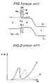
- FIG.1 is a schematic energy band diagram of the conventional RBT.
- a quantum well layer QW is inserted between an n-AlGaAs emitter layer E and a p+-GaAs base layer B.
- the quantum well layer QW consists of a GaAs well layer W and AlAs barrier layers PB positioned on both sides of the GaAs well layer W.
- An n-GaAs collector layer C is adjacent to the p+-GaAs base layer B.
- RLC and RLV represent resonant energy levels of electrons and holes, respectively, and e indicates electrons.
- the illustrated energy band diagram may be obtained with a base-emitter voltage V BE of approximately 1.6 (V) applied across the base and emitter.
- FIG.2 is a graph of current-voltage characteristics of the RBT having the energy band diagram shown in FIG.1.
- the horizontal axis represents the base-emitter voltage V BE
- the vertical axis represents the collector current I C and the base current I B .
- a curved solid line is a characteristic line of the collector current I C
- a curved broken line is a characteristic line of the base current I B .
- there are peaks in both the collector current I C and the base current I B This means that resonant-tunneling currents flow in the peak current regions.
- electrons are the carrier of the collector current I C and holes are the carrier of the base current I B .
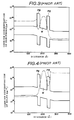
- FIGS.3 and 4 are schematic energy band diagrams for explaining storage of the carriers of electrons and holes in the well layer W, respectively.
- the horizontal axes of FIGS.3 and 4 represent a distance measured from the emitter side, and the vertical axes represent a carrier concentration.
- a dotted chain line in FIG.3 shows an electron concentration and a dotted chain line in FIG.4 shows a hole concentration.
- the electron concentration and the hole concentration are increased in the well layer W.
- increases in the concentration of electrons and holes do not occur at the same time.
- one object of the present invention is intended to simultaneously produce the occurrence of the resonant-tunneling of electrons and holes.
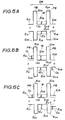
- FIGS.5A through 5C are schematic energy band diagrams of a structure where the quantum well layer QW is sandwiched by an n-semiconductor layer and a p-semiconductor layer.
- the energy band diagrams are illustrated in a state where a bias voltage which corresponds to the difference between Fermi levels of the n- and p-semiconductor layers is applied across the n- and p-semiconductor layers.
- the same reference symbols as those in the previous figures indicate the same elements or have the same meanings.
- a symbol Ec1 represents an energy level at the bottom of the conduction band of the n-semiconductor layer.
- Ev1 represents an energy level at the top of the valence band of the n-semiconductor layer.
- Ec2 and Ev2 represent energy levels at the bottom and top of conduction and valence bands of the barrier layer PB on the side of the n-semiconductor layer, respectively.
- the energy level Ec2 is larger than the energy level Ec1
- energy level Ev2 is smaller than energy level Ev1.
- Ec3 represents a resonant energy level of electrons in the conduction band of the well layer W.
- Ev3 represents a resonant energy level of holes in the valence band of the well layer W.
- the energy level Ec3 is smaller than the energy level Ec2, and the energy level Ev3 is larger than the energy level Ev2.
- Ec4 and Ev4 represent energy levels at the bottom and top of conduction and valence bands of the barrier layer PB on the side of the p-semiconductor layer, respectively.
- the energy level Ec4 is larger than the energy level Ec3, and the energy level Ev4 is smaller than the energy level Ev3.
- Ec5 represents an energy level at the bottom of the conduction band of the p-semiconductor layer.
- Ev5 represents an energy level at the top of the valence band of the p-semiconductor layer.
- the energy level Ec5 is smaller than the energy level Ec4, and the energy level Ev5 is larger than the energy level Ev4.
- ⁇ Ec is a difference (absolute value) between the resonant energy level Ec3 and an energy level Ec3 ⁇ at the bottom of the conduction band of the well layer W. It is further assumed that ⁇ Ev is a difference (absolute value) between the resonant energy level Ev3 and an energy level Ev3 ⁇ at the top of the valence band of the well layer W.
- the energy level Ec1 is selected so that an absolute value of a difference D1 between the energy levels Ec1 and Ec3 becomes nearly equal to an absolute value of a difference D2 between the energy levels Ev3 and Ev5.
- the band gap of the n-semiconductor layer is made wider so as to satisfy the above condition.
- the energy level Ev5 is selected so that an absolute value of a difference D4 between the energy levels Ev3 and Ev5 becomes nearly equal to an absolute value of a difference D3 between Ec1 and Ec3.
- the band gap of the p-semiconductor layer is made wider so as to satisfy the above condition.
- the present invention it becomes possible to provide semiconductor devices such as a diode, an npn transistor and a pnp transistor, in which the resonant-tunneling of electrons and the resonant-tunneling of holes may occur at the same time with a suitable voltage applied across the n-and p-semiconductor layers.
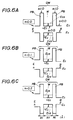
- FIGS.6A through 6C are schematic energy band diagrams each having different x values of the Al x Ga 1-x As emitter layer E in the RBT.
- Specifications of essential elements of the RBT having the energy band diagrams shown in FIGS.6A through 6C are as follows:
- FIGS.7, 8 and 9 show current-voltage characteristics which correspond to FIGS.6A, 6B and 6C, respectively.
- the horizontal axis represents an applied voltage and the vertical axis represents a current.
- a long broken line indicated by a character e is a characteristic line relating to the current caused by the motion of electrons.
- a dotted chain line indicated by a character Lh is a characteristic line relating to the current caused by the motion of light holes.
- a short broken line indicated by a character Hh is a characteristic line relating to the current due to heavy holes.
- a solid line indicated by a character T is a characteristic line relating to a total current.
- the measurement results indicate that occurrence of the resonant-tunneling of electrons and the resonant-tunneling of holes may be controlled by selecting the mole fraction x of the emitter layer E.
- the simultaneous occurrence of both the resonant-tunneling of electrons and the resonant-tunneling of holes are found when the mole fraction x of the emitter layer E is equal to 0.0.
- the simultaneous occurrence can also be obtained by setting a different mole fraction x of the emitter layer E by varying parameters other than the mole fraction x , for example the width of the well layer W.
- the above measurement results prove that it is possible to produce the occurrence of the resonant-tunneling of electrons and the resonant-tunneling of holes at the same time and to thereby store and recombine electrons and holes in the well layer W by selecting one or more of the above mentioned means (1) to (7). Accordingly, the current density can be improved.
- the semiconductor device according to the present invention is suitable for high-speed light communications.
- the semiconductor device of the present invention may operate as the conventional RBT by controlling the base-emitter voltage. For this reason, the present semiconductor device is suitable for fabrication of an optoelectronic integrated circuit (generally abbreviated as an OEIC).
- FIG.10 shows a schematic cross section of an example of a semiconductor device according to the present invention.
- the illustrated semiconductor device is one example of an npn transistor which may be obtained according to the present invention.
- a quantum well layer 15 is inserted between p+-GaAs base layer 13 and an n-GaAs emitter layer 17 through a non-doped GaAs spacer layer 14 and a non-doped GaAs spacer layer 16, respectively.
- the quantum well layer 15 consists of a GaAs well layer 15W and AlAs potential barrier layers 15B1 and 15B2 which are positioned on the bottom and top surfaces of the GaAs well layer 15W, respectively.
- the quantum well layer 15 may be grown by molecular beam epitaxy (MBE), for example.
- MBE molecular beam epitaxy
- the spacer layer 14 is provided to prevent impurities which are doped in the p+-GaAs base layer 13, beryllium (Be), for example, from diffusing into the barrier layer 15B1 and to thereby prevent the diffused impurities from exerting the impurity scattering effect on electrons and holes.
- the spacer 1ayer 16 is provided to prevent impurities doped in the n-GaAs emitter layer 17, silicon (Si), for example, from diffusing into the barrier layer 15B2 and to prevent occurrence of the impurity scattering effect.
- the p+-GaAs base layer 13 is deposited on an n-GaAs collector layer 12.
- This structure may be grown on an n+-GaAs substrate 11 by molecular beam epitaxy (MBE), for example.
- MBE molecular beam epitaxy
- a collector electrode 21 is metallized on the bottom surface of the n+-GaAs substrate 11.
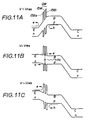
- FIGS.11A through 11C are schematic energy band diagrams for explaining operation of the semiconductor device having the structure shown in FIG.10.
- the same reference symbols as those in the previous figures indicate the same elements or have the same meanings.
- FIG.12 shows a light output versus a voltage characteristic of the semiconductor device shown in FIG.10.
- the horizontal axis represents the voltage V applied across the base and emitter, and the vertical axis represents the light output P.
- the characteristic diagram shows that that when the applied voltage V becomes nearly equal to the voltage Vres at which the device is in the resonant state, the light output P appears. This light-emitting phenomenon corresponds to the operative state shown in FIG.11B.
- FIG.13 shows schematic current-voltage characteristics in the operative state shown in FIG.11B.
- the horizontal axis represents the voltage V applied across the base and emitter, and the vertical axis represents the current I.
- a solid line shows the collector current I C and a dotted chain line shows the base current I B .
- the diagram indicates that both the collector current I C and the base current I B have peaks at the voltage of approximately 1.8 (V). This means that the resonant-tunneling of electrons and the resonant-tunneling of holes occur at this time.
- the structure shown in FIG.10 can operate as a diode, which exists between the base and emitter. It is also possible to configure only the diode by eliminating the layers 11, 12 and 21.
- FIG.14A is a schematic energy band diagram of a semiconductor device corresponding to the energy band diagram shown in FIG.5B where the resonant energy level of the electrons, Ec3 is larger than the energy level of the holes, Ev3.
- An n-semiconductor layer is made of (InGaAs) 0.86 (InAlAs) 0.14 .
- a p-semiconductor layer is made of In 0.53 Ga 0.47 As.
- a quantum well layer QW consists of an In 0.53 Ga 0.47 As well layer W and In 0.52 Al 0.48 As potential barrier layers PB.
- the In 0.53 Ga 0.47 As well layer W is 38 ⁇ wide and the In 0.52 Al 0.48 As potential barrier layers PB are each 44 ⁇ wide.
- the resonant energy levels of the electrons and holes Ec3 and Ev3 in the well layer W thus structured are equal to 0.175 (eV) and 0.084 (eV), respectively. That is, the energy difference ⁇ Ec is larger than the energy difference ⁇ Ev.
- the n-semiconductor layer is made of (InGaAs) 0.86 (InAlAs) 0.14 so that the band gap becomes wider to satisfy the condition discussed in the foregoing.
- the impurity concentration of the n-semiconductor layer is 1 x 10¹⁸ (cm ⁇ 3).
- the impurity concentration of the p-semiconductor layer is 5 x 10¹⁸ (cm ⁇ 3).
- FIG.14B shows current-voltage characteristics of the semiconductor device having the structure in FIG.14A.
- the horizontal axis represents the voltage applied across the p- and n-semiconductor layers, and the vertical axis represents the current.
- the illustrated current-voltage characteristics show that the resonant-tunneling of the electrons and the resonant-tunneling of the (light) holes occur at the same time when the voltage around 1.16 (V) is applied to the device.
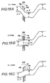
- FIGS.15A through 15C are schematic energy band diagrams of a pnp transistors according to the present invention.
- the illustrated transistor has the condition shown in FIG.5A in which the energy difference ⁇ Ec is equal to the energy difference ⁇ Ev.
- the resonant-tunneling of electrons and the resonant-tunneling of holes occur at the same time.
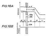
- FIGS.16A is a schematic energy band diagram of the semiconductor device shown in FIG.10 where the resonant-tunneling of the electrons and holes occurs at the same time
- FIG.16B shows a refractive index distribution corresponding to the energy band diagram shown in FIG.16A.
- the refractive indexes of the AlAs barrier layers 15B1 and 15B2 are smaller than that of the GaAs well layer 15W in which the light may be emitted. Therefore, in this regard, the AlAs barrier layers 15B1 and 15B2 are suitable for a light confining layer.
- the thickness of each of the AlAs barrier layers 15B1 and 15B2 is approximately 2 (nm) and is therefore very thin.
- the AlAs barrier layers 15B1 and 15B2 cannot provide a sufficient light confining function. That is, the AlAs barrier layers 15B1 and 15B2 cannot effectively guide the light emitted in the GaAs well layer 15W towards an end surface of the device. It is considered that a thickness of approximately 100 nm of the barrier layers is necessary to establish a satisfactory light confining effect. However, setting the thickness to 100 nm or over is actually impossible, because such setting acts to degrade the performance of the resonant-tunneling.
- a modification described below intends to form a light waveguide which guides the light emitted in the well layer towards the end surface of the device by constituting a light confining layer, so that the light-emitting efficiency can be improved.
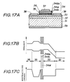
- FIG.17A shows a schematic cross section of a modification having the features mentioned above
- FIG.17B shows a schematic energy band diagram of the modification shown in FIG.17A where the bias voltage is applied
- FIG.17C shows a refractive index distribution of the modification shown in FIG.17A.
- a quantum well resonator 34 is inserted between a base layer 33 and an emitter layer 35.
- the quantum well layer 34 consists of a GaAs well layer 34W and AlAs potential barrier layers 34B1 and 34B2 which are positioned on the bottom and top surfaces of the GaAs well layer 34W, respectively.
- the quantum well layer 34 may be grown by MOCVD, for example.
- the base layer 33 is mounted on an n-GaAs collector layer 32. This structure is grown on an n+-GaAs substrate 31 by MBE, for example.
- On the top surface of the p+-GaAs base layer 33 there are metallized base electrodes 38.
- a collector electrode 39 is metallized on the bottom surface of the n+-GaAs substrate 31.
- the base layer 33 is desired to have the band gap energy and the refractive index similar to those of an In 0.5 Al 0.5 As mixed crystal.
- the In 0.5 Al 0.5 As mixed crystal is not suitable for a material of the base layer 33. This is because the lattice constant of the In 0.5 Al 0.5 As mixed crystal differs from that of GaAs forming the substrate 31. That is, the lattice mismatching occurs between the GaAs substrate 31 and the base layer 33 of the In 0.5 Al 0.5 As mixed crystal.
- the band gap and the refractive index of the base layer 33 are achieved by use of an InAs/AlAs strained-layer superlattice structure, which is a mixed crystal of In 0.5 Al 0.5 As.
- This mixed crystal has a periodical structure of alternatively stacked InAs layers and AlAs layers. Broken lines shown in FIG.17A indicate the In 0.5 Al 0.5 As mixed crystal.
- An intermediate part of the emitter layer 35 is made of Al x Ga 1-x As where the mole fraction x is equal to 0.3.
- the mole fraction x of the emitter layer 35 is graded from 0.0 to 0.3 in the range of 70 (nm) from the interface with the barrier layer 34B2.
- the band gap energy in the vicinity of the interface with the quantum well structure 34 is graded, as shown in FIG.17C. This is because there is a possibility that an abrupt band change would generate a spike.
- the AlGaAs mole fraction x of the emitter layer 35 is graded from 0.3 to 0.0 in the range of 70 (nm) from the interface with the GaAs emitter contact layer 36.
- the emitter layer 35 thus structured has the refractive index shown in FIG.17C. As shown in this figure, the refractive index of the emitter layer 35 is smaller than that of the well layer 34W. This means that the emitter layer 35 forms the light confining layer.
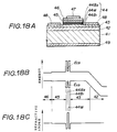
- FIGS.18A through 18C shown another example of the semiconductor device having a light confining layer according to the present invention.
- a quantum well resonator 44 is inserted between an In 0.52 Al 0.48 As base layer 43 and an In 0.52 Al 0.48 As emitter layer 45.
- the quantum well layer 44 consists of a GaAs well layer 44W and AlAs potential barrier layers 44B1 and 44B2 which are positioned on the bottom and top surfaces of the GaAs well layer 44W, respectively.
- the quantum well layer 44 may be grown by MOCVD, for example.
- the In 0.52 Al 0.48 As base layer 43 is deposited on the top of an In 0.52 Al 0.48 As collector layer 42. This structure is grown on an InP substrate 41 by MBE, for example.
- On the top surface of the In 0.52 Al 0.48 As base layer 43 there are metallized base electrodes 48.
- a collector electrode 49 is metallized on the bottom surface of the In 0.52 Al 0.48 As substrate 41.
- FIGS.18B and 18C The band gap energy and the refractive index of each layer are shown in FIGS.18B and 18C.
- FIG.18C reveals that there are formed the light confining layers having the refractive index smaller than that of the well layer 44W in the vicinity of the well layer 44W.
- the resonant-tunneling of electrons and the resonant-tunneling of holes can occur at the same time, because the device satisfies the condition shown in FIG.5A.
Landscapes
- Engineering & Computer Science (AREA)
- Chemical & Material Sciences (AREA)
- Nanotechnology (AREA)
- Physics & Mathematics (AREA)
- Mathematical Physics (AREA)
- Theoretical Computer Science (AREA)
- Crystallography & Structural Chemistry (AREA)
- Bipolar Transistors (AREA)
Claims (15)
- Halbleitervorrichtung mit einer ersten, n-leitenden Halbleiterschicht (17) mit einem Energieniveau Ec₁ am unteren Ende ihres Leitungsbands und einem Energieniveau Ev₁ am oberen Ende ihres Valenzbands; mit einer zweiten Halbleiterschicht (15B₂) mit einem Energieniveau Ec₂ am unteren Ende ihres Leitungsbands, das größer als Ec₁ ist, und mit einem Energieniveau Ev₂ am oberen Ende ihres Valenzbands, das kleiner als Ev₁ ist, wobei die zweite Schicht auf einer Oberfläche der ersten Schicht aufgebracht ist; mit einer dritten Halbleiterwannenschicht (15W) mit einem Schwingungsenergieniveau Ec₃ der Elektronen in ihrem Leitungsband, das kleiner als Ec₂ ist, und mit einem Schwingungsenergieniveau Ev₃ der Löcher in ihrem Valenzband, das größer als Ev₂ ist, wobei die dritte Schicht auf einer Oberfläche der zweiten Schicht aufgebracht ist; mit einer vierten Halbleiterschicht (15B₁) mit einem Energieniveau Ec₄ am unteren Ende ihres Leitungsbands, das größer als Ec₃ ist, und mit einem Energieniveau Ev₄ am oberen Ende ihres Valenzbands, das kleiner als Ev₃ ist, wobei die vierte Schicht auf einer Oberfläche der dritten Schicht aufgebracht ist; und mit einer fünften, p-leitenden Halbleiterschicht (13) mit einem Energieniveau Ec₅ am unteren Ende ihres Leitungsbands, das kleiner als Ec₄ ist, und mit einem Energieniveau Ev₅ am oberen Ende ihres Valenzbands, das größer als Ev₄ ist, wobei die fünfte Schicht auf einer Oberfläche der vierten Schicht aufgebracht ist; wobei |Ec₃ - Ec₁| zur Erzielung einer gleichzeitigen Schwingung von Elektronen und Löchern in etwa |Ev₃ - Ev₅| entspricht.
- Halbleitervorrichtung nach Anspruch 1,
dadurch gekennzeichnet, daß dann, wenn eine Energie ΔEc, bei der es sich um die Differenz zwischen dem Schwingungsenergieniveau Ec₃ und einem Energieniveau Ec₃' am unteren Ende des Leitungsbands der dritten Schicht handelt, einer Energie ΔEv entspricht, bei der es sich um die Differenz zwischen dem Schwingungsenergieniveau Ev₃ und einem Energieniveau Ev₃' am oberen Ende des Valenzbands der dritten Schicht handelt, die Bandabstandsenergie der ersten Schicht in etwa der der fünften Schicht entspricht. - Halbleitervorrichtung nach Anspruch 1,
dadurch gekennzeichnet, daß dann, wenn eine Energie ΔEc, bei der es sich um die Differenz zwischen dem Schwingungsenergieniveau Ec₃ und einem Energieniveau Ec₃' am unteren Ende des Leitungsbands der dritten Schicht handelt, größer als eine Energie ΔEv ist, bei der es sich um die Differenz zwischen dem Schwingungsenergieniveau Ev₃ und einem Energieniveau Ev₃' am oberen Ende des Valenzbands der dritten Schicht handelt, die Bandabstandsenergie der ersten Schicht größer als die der fünften Schicht eingestellt ist. - Halbleitervorrichtung nach Anspruch 1,
dadurch gekennzeichnet, daß dann, wenn eine Energie ΔEc, bei der es sich um die Differenz zwischen dem Schwingungsenergieniveau Ec₃ und einem Energieniveau Ec₃' am unteren Ende des Leitungsbands der dritten Schicht handelt, kleiner als eine Energie ΔEv ist, bei der es sich um die Differenz zwischen dem Schwingungsenergieniveau Ev₃ und einem Energieniveau Ev₃' am oberen Ende des Valenzbands der dritten Schicht handelt, die Bandabstandsenergie der ersten Schicht kleiner als die der fünften Schicht eingestellt ist. - Halbleitervorrichtung nach einem der Ansprüche 1 bis 4,
dadurch gekennzeichnet, daß es sich bei der zweiten, dritten und vierten Schicht um Quantenwannenschichten (15) handelt. - Halbleitervorrichtung nach einem der Ansprüche 1 bis 5,
dadurch gekennzeichnet, daß die zweite, dritte und vierte Schicht undotiert sind. - Halbleitervorrichtung nach einem der Ansprüche 1 bis 6,
dadurch gekennzeichnet, daß die Brechungsindices der ersten und der fünften Schicht kleiner als der Brechungsindex der dritten Schicht sind. - Halbleitervorrichtung nach einem der Ansprüche 1 bis 6,
dadurch gekennzeichnet, daß die erste, dritte und fünfte Schicht aus GaAs gebildet sind und die zweite und die vierte Schicht aus AlAs gebildet sind. - Halbleitervorrichtung nach einem der ansprüche 1 bis 7,
dadurch gekennzeichnet, daß die erste Schicht aus (InGaAs)1-x(InAlAs)x gebildet ist, die zweite und die vierte Schicht aus InyAl1-yAs gebildet sind und die dritte und die fünfte Schicht aus InzGa1-zAs gebildet sind. - Halbleitervorrichtung nach einem der Ansprüche 1 bis 7,
dadurch gekennzeichnet, daß die erste Schicht aus AlxGa1-xAs gebildet ist, die zweite und die vierte Schicht aus AlAs gebildet sind, die dritte Schicht aus GaAs gebildet ist und die fünfte Schicht aus einer InAs/AlAs-Übergitterkonstruktion mit Schichtverspannung gebildet ist. - Halbleitervorrichtung nach Anspruch 10,
dadurch gekennzeichnet, daß der Molanteil x der ersten Schicht aus AlxGa1-xAs abgestuft ist. - Halbleitervorrichtung nach einem der Ansprüche 1 bis 7,
dadurch gekennzeichnet, daß die erste Schicht aus InxAl1-xAs gebildet ist, die zweite und die vierte Schicht aus AlAs gebildet sind, die dritte Schicht aus GaAs gebildet ist und die fünfte Schicht aus InyAl1-yAs gebildet ist. - Halbleitervorrichtung nach einem der Ansprüche 1 bis 12,
dadurch gekennzeichnet, daß es sich bei der Halbleitervorrichtung um eine Diode, bei der ersten Schicht um eine Kathode und bei der fünften Schicht um eine Anode handelt. - Halbleitervorrichtung nach einem der Ansprüche 1 bis 12,
dadurch gekennzeichnet, daß die Halbleitervorrichtung ferner eine sechste, n-leitende Halbleiterschicht (12) aufweist, die auf einer Oberfläche der fünften Schicht aufgebracht ist, so daß ein pnp-Transistor gebildet ist, wobei die erste Schicht den Emitter, die fünfte Schicht die Basis und die sechste Schicht den Kollektor bildet. - Halbleitervorrichtung nach einem der Ansprüche 1 bis 12,
dadurch gekennzeichnet, daß die Halbleitervorrichtung ferner eine sechste, n-leitende Halbleiterschicht aufweist, die auf einer Oberfläche der ersten Schicht aufgebracht ist, so daß ein pnp-Transistor gebildet ist, wobei die erste Schicht die Basis, die fünfte Schicht den Emitter und die sechste Schicht den Kollektor bildet.
Applications Claiming Priority (4)
| Application Number | Priority Date | Filing Date | Title |
|---|---|---|---|
| JP61249572A JPS63104471A (ja) | 1986-10-22 | 1986-10-22 | 半導体装置 |
| JP249572/86 | 1986-10-22 | ||
| JP61276953A JPS63129678A (ja) | 1986-11-20 | 1986-11-20 | 半導体装置 |
| JP276953/86 | 1986-11-20 |
Publications (3)
| Publication Number | Publication Date |
|---|---|
| EP0268512A2 EP0268512A2 (de) | 1988-05-25 |
| EP0268512A3 EP0268512A3 (en) | 1989-10-25 |
| EP0268512B1 true EP0268512B1 (de) | 1994-05-25 |
Family
ID=26539369
Family Applications (1)
| Application Number | Title | Priority Date | Filing Date |
|---|---|---|---|
| EP87402369A Expired - Lifetime EP0268512B1 (de) | 1986-10-22 | 1987-10-21 | Halbleiterschaltung mit resonantem Tunnelungseffekt |
Country Status (3)
| Country | Link |
|---|---|
| US (1) | US5031005A (de) |
| EP (1) | EP0268512B1 (de) |
| DE (1) | DE3789891D1 (de) |
Families Citing this family (10)
| Publication number | Priority date | Publication date | Assignee | Title |
|---|---|---|---|---|
| US4973858A (en) * | 1986-07-18 | 1990-11-27 | Ibm Corporation | Resonant tunneling semiconductor devices |
| JPS63140570A (ja) * | 1986-12-03 | 1988-06-13 | Hitachi Ltd | 半導体装置 |
| US5206524A (en) * | 1988-09-28 | 1993-04-27 | At&T Bell Laboratories | Heterostructure bipolar transistor |
| NL9200500A (nl) * | 1991-04-17 | 1992-11-16 | Imec Inter Uni Micro Electr | Halfgeleider-inrichting, licht uitzendende diode en transistoropbouw, gebruikmakend van resonante tunneling. |
| JPH05304290A (ja) * | 1992-04-28 | 1993-11-16 | Nec Corp | オーミック電極 |
| US5326985A (en) * | 1992-09-28 | 1994-07-05 | Motorola, Inc. | Bipolar doped semiconductor structure and method for making |
| US6229153B1 (en) * | 1996-06-21 | 2001-05-08 | Wisconsin Alumni Research Corporation | High peak current density resonant tunneling diode |
| GB2341974A (en) * | 1998-09-22 | 2000-03-29 | Secr Defence | Semiconductor device incorporating a superlattice structure |
| JP2001077352A (ja) * | 1999-09-07 | 2001-03-23 | Sony Corp | 半導体素子およびその製造方法 |
| US7099362B2 (en) * | 2003-11-14 | 2006-08-29 | Finisar Corporation | Modulation doped tunnel junction |
Family Cites Families (4)
| Publication number | Priority date | Publication date | Assignee | Title |
|---|---|---|---|---|
| CA1237824A (en) * | 1984-04-17 | 1988-06-07 | Takashi Mimura | Resonant tunneling semiconductor device |
| JPS6158268A (ja) * | 1984-08-30 | 1986-03-25 | Fujitsu Ltd | 高速半導体装置 |
| JPH0611056B2 (ja) * | 1985-12-03 | 1994-02-09 | 富士通株式会社 | 高速半導体装置 |
| US4780749A (en) * | 1986-07-01 | 1988-10-25 | Hughes Aircraft Company | Double barrier tunnel diode having modified injection layer |
-
1987
- 1987-10-21 EP EP87402369A patent/EP0268512B1/de not_active Expired - Lifetime
- 1987-10-21 DE DE3789891T patent/DE3789891D1/de not_active Expired - Lifetime
- 1987-10-21 US US07/111,018 patent/US5031005A/en not_active Expired - Fee Related
Also Published As
| Publication number | Publication date |
|---|---|
| EP0268512A2 (de) | 1988-05-25 |
| DE3789891D1 (de) | 1994-06-30 |
| EP0268512A3 (en) | 1989-10-25 |
| US5031005A (en) | 1991-07-09 |
Similar Documents
| Publication | Publication Date | Title |
|---|---|---|
| US5237581A (en) | Semiconductor multilayer reflector and light emitting device with the same | |
| EP0133342B1 (de) | Halbleiterstruktur mit Übergitter hoher Trägerdichte | |
| AU2010203817B2 (en) | Light emitting and lasing semiconductor devices and methods | |
| US5010374A (en) | Quantum well laser utilizing an inversion layer | |
| KR19980034078A (ko) | 핫 전자 장치(Hot Electron Device) 및 공진 터널링 핫 전자 장치 | |
| US5349201A (en) | NPN heterojunction bipolar transistor including antimonide base formed on semi-insulating indium phosphide substrate | |
| GB2285172A (en) | Semiconductor laser device | |
| EP0975073A1 (de) | Halbleiterlaser | |
| EP0227865B1 (de) | Lichtemittierende Halbleiterschaltung | |
| JPH02231777A (ja) | 共鳴トンネル光電素子 | |
| EP0268512B1 (de) | Halbleiterschaltung mit resonantem Tunnelungseffekt | |
| US5164797A (en) | Lateral heterojunction bipolar transistor (LHBT) and suitability thereof as a hetero transverse junction (HTJ) laser | |
| US5003366A (en) | Hetero-junction bipolar transistor | |
| US5107514A (en) | Semiconductor optical element | |
| US5422902A (en) | BeTe-ZnSe graded band gap ohmic contact to p-type ZnSe semiconductors | |
| US5337326A (en) | Semiconductor laser device with compressively stressed barrier layer | |
| KR920006434B1 (ko) | 공진 터널링 장벽구조장치 | |
| US7986721B2 (en) | Semiconductor optical device including a PN junction formed by a second region of a first conductive type semiconductor layer and a second conductive type single semiconductor layer | |
| US5280182A (en) | Resonant tunneling transistor with barrier layers | |
| JPH0740570B2 (ja) | 共鳴トンネリング装置 | |
| US5497012A (en) | Unipolar band minima devices | |
| EP0186301B1 (de) | Halbleiteranordnung mit grosser Geschwindigkeit | |
| US7323722B2 (en) | Semiconductor optical device | |
| US7838893B2 (en) | Semiconductor optical device | |
| US7208774B2 (en) | Semiconductor optical device |
Legal Events
| Date | Code | Title | Description |
|---|---|---|---|
| PUAI | Public reference made under article 153(3) epc to a published international application that has entered the european phase |
Free format text: ORIGINAL CODE: 0009012 |
|
| AK | Designated contracting states |
Kind code of ref document: A2 Designated state(s): DE FR GB |
|
| PUAL | Search report despatched |
Free format text: ORIGINAL CODE: 0009013 |
|
| AK | Designated contracting states |
Kind code of ref document: A3 Designated state(s): DE FR GB |
|
| 17P | Request for examination filed |
Effective date: 19900412 |
|
| 17Q | First examination report despatched |
Effective date: 19910814 |
|
| GRAA | (expected) grant |
Free format text: ORIGINAL CODE: 0009210 |
|
| AK | Designated contracting states |
Kind code of ref document: B1 Designated state(s): DE FR GB |
|
| PG25 | Lapsed in a contracting state [announced via postgrant information from national office to epo] |
Ref country code: DE Effective date: 19940525 |
|
| REF | Corresponds to: |
Ref document number: 3789891 Country of ref document: DE Date of ref document: 19940630 |
|
| ET | Fr: translation filed | ||
| PG25 | Lapsed in a contracting state [announced via postgrant information from national office to epo] |
Ref country code: GB Effective date: 19941021 |
|
| PLBE | No opposition filed within time limit |
Free format text: ORIGINAL CODE: 0009261 |
|
| STAA | Information on the status of an ep patent application or granted ep patent |
Free format text: STATUS: NO OPPOSITION FILED WITHIN TIME LIMIT |
|
| 26N | No opposition filed | ||
| GBPC | Gb: european patent ceased through non-payment of renewal fee |
Effective date: 19941021 |
|
| PGFP | Annual fee paid to national office [announced via postgrant information from national office to epo] |
Ref country code: FR Payment date: 19951010 Year of fee payment: 9 |
|
| PG25 | Lapsed in a contracting state [announced via postgrant information from national office to epo] |
Ref country code: FR Effective date: 19970630 |
|
| REG | Reference to a national code |
Ref country code: FR Ref legal event code: ST |