EP0265271A2 - Elektronischer Verschluss für eine elektronische Kamera und Verfahren zur Verwendung eines CCD Bildsensors als elektronischer Verschluss für eine solche Kamera - Google Patents
Elektronischer Verschluss für eine elektronische Kamera und Verfahren zur Verwendung eines CCD Bildsensors als elektronischer Verschluss für eine solche Kamera Download PDFInfo
- Publication number
- EP0265271A2 EP0265271A2 EP87309365A EP87309365A EP0265271A2 EP 0265271 A2 EP0265271 A2 EP 0265271A2 EP 87309365 A EP87309365 A EP 87309365A EP 87309365 A EP87309365 A EP 87309365A EP 0265271 A2 EP0265271 A2 EP 0265271A2
- Authority
- EP
- European Patent Office
- Prior art keywords
- substrate
- region
- conductivity type
- charge accumulating
- imager device
- Prior art date
- Legal status (The legal status is an assumption and is not a legal conclusion. Google has not performed a legal analysis and makes no representation as to the accuracy of the status listed.)
- Granted
Links
Images
Classifications
-
- H—ELECTRICITY
- H10—SEMICONDUCTOR DEVICES; ELECTRIC SOLID-STATE DEVICES NOT OTHERWISE PROVIDED FOR
- H10F—INORGANIC SEMICONDUCTOR DEVICES SENSITIVE TO INFRARED RADIATION, LIGHT, ELECTROMAGNETIC RADIATION OF SHORTER WAVELENGTH OR CORPUSCULAR RADIATION
- H10F39/00—Integrated devices, or assemblies of multiple devices, comprising at least one element covered by group H10F30/00, e.g. radiation detectors comprising photodiode arrays
- H10F39/10—Integrated devices
- H10F39/12—Image sensors
- H10F39/15—Charge-coupled device [CCD] image sensors
- H10F39/153—Two-dimensional or three-dimensional array CCD image sensors
-
- H—ELECTRICITY
- H10—SEMICONDUCTOR DEVICES; ELECTRIC SOLID-STATE DEVICES NOT OTHERWISE PROVIDED FOR
- H10F—INORGANIC SEMICONDUCTOR DEVICES SENSITIVE TO INFRARED RADIATION, LIGHT, ELECTROMAGNETIC RADIATION OF SHORTER WAVELENGTH OR CORPUSCULAR RADIATION
- H10F39/00—Integrated devices, or assemblies of multiple devices, comprising at least one element covered by group H10F30/00, e.g. radiation detectors comprising photodiode arrays
- H10F39/10—Integrated devices
- H10F39/12—Image sensors
- H10F39/15—Charge-coupled device [CCD] image sensors
- H10F39/158—Charge-coupled device [CCD] image sensors having arrangements for blooming suppression
Definitions
- This invention relates to solid imager devices, and to methods of utilizing a solid state imager device as an electronic shutter, for example, for an electronic camera such as a video camera or an electronic still camera.
- a solid state imager device be able to control its exposure time by electronic means provided therein, so that when the imager device is used in, for example, a video camera, the use of a mechanical shutter as hitherto proposed, is unnecessary. Without a mechanical shutter, a video camera could be made smaller, lighter, and more cheaply.
- This imager device has one of the two exposure times chosen to be 1/30 second, which is equal to one frame period in the NTSC television system, and the other exposure time chosen to be about 1/2000 second, which is equal to a vertical blanking period.
- this imager device is limited in that it only allows selection between two exposure times so that, even when a video camera is equipped with such an imager device, it still requires a mechanical shutter. Moreover, since a high speed transfer is required to discharge the signal charges accumulated before a vertical blanking period to the vertical register, the imager device consumes excessive electric power.
- a solid state imager device comprising: a semiconductor substrate of first conductivity type; a region of second conductivity type formed on said substrate; and a signal charge accumulating region formed on a surface side of said second conductivity type region; characterized by: means for applying a predetermined voltage to said substrate thereby to discharge signal charges accumulated in said signal charge accumulating region to said substrate.
- a method of utilizing a solid state imager device as an electronic shutter for an electronic camera comprising the step of applying voltage potential across a semiconductor substrate of a first conductivity type and a region of a second conductivity type formed on said substrate, thereby to discharge signal charges accumulated in a signal charge accumulating region formed on a surface side of said second conductivity type region to said substrate.
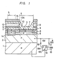
- the solid state image device of Figure 1 comprises an N type silicon substrate 1 upon which a light receiving section 4, a vertical register section 5, a horizontal register section (not shown) and an output section (not shown) are formed, so as to constitute a so-called interline transfer charge coupled device (CCD) type imager device.
- a P type region 2 On the surface of the substrate 1 there is deposited, for example, by epitaxial growth techniques, a P type region 2.
- An N ⁇ type region 6 is deposited on the surface of the P type region 2.
- the light receiving section 4 is formed of a shallow P++ type region 7 formed in a surface region of the N ⁇ type region 6 and an N+ type region 3 is formed beneath the P++ type region 7 to constitute a signal charge accumulating region.
- a P+ type region 8 constituting a channel stopper section formed adjacent to the P++ type region 7 and the N+ type region 3.
- An insulating layer 9 made of SiO2 is deposited on the P++ type region 7.
- the vertical register section 5 is formed such that an N+ type region 11, which constitutes a signal charge transfer region, is formed adjacent to a P type region 10, which constitutes a read-out gate region.
- a transfer electrode 13 made of polysilicon and another insulating layer 12 made of Si3N4 are formed above the N+ type region 11 within the SiO2 insulating layer 9.
- One end portion of the transfer electrode 13 is also used as a read-out gate electrode 13A.
- a P type region 14 is formed, for preventing smear, beneath the N+ type region 11.
- An aluminium layer 15 for shielding light is deposited above the transfer electrode 13 above the insulating layer 9.
- transfer electrodes 13 Although only two of the transfer electrodes 13 are illustrated in Figure 1, there are disposed a predetermined number of transfer electrodes 13 such that the vertical register section 5 is driven in known manner by a four-phase drive.
- the horizontal register section and the output section which are not illustrated in the drawing, are of known form.
- the negative voltage terminals of direct current (DC) power supply sources 16 and 17 are commonly connected to the P type region 2 and earthed.
- the positive voltage terminals of the sources 16 and 17 are connected to first and second fixed contacts 18A and 18B, respectively, of a switching circuit 18.
- a movable contact 18C of the switching circuit 18 is connected to the substrate 1.
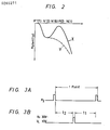
- An output voltage V L from the source 16 is selected to be a value, for example, 10 volts, such that when the voltage V L is applied to the substrate 1, the potential in the P type region 2 becomes slightly lower than the potential of the shallow P++ type region 7 on the surface of the N+ type region 3, as shown by a solid line X in Figure 2, so that signal charges can be accumulated in the N+ type signal charge accumulating region 3 and blooming can be effectively suppressed.
- An output voltage V H from the source 17 is selected to be a value, for example 30 volts, such that when the voltage V H is applied to the substrate 1, the potential in the P type region 2 becomes lower than the potential in the signal charge accumulating region 3, as is shown by a broken line Y in Figure 2, so that the signal charges accumulated in the signal charge accumulating region 3 can be discharged to the substrate 1.
- Switching of the switching circuit 18 can be controlled by a control signal supplied thereto through a control signal input terminal 19.
- a read-out pulse P2 as shown in Figure 3A, is supplied to the read-out gate electrode 13A while the output voltage V L from the source 16 is applied to the substrate 1, signal charges accumulated in the signal charge accumulating region 3 are read out to the vertical register section 5. Therefore, in the present embodiment, the read-out pulse R2 is supplied to the read-out gate electrode 13A at every field within the vertical retrace.
- the exposure time of the imager device becomes the period t1, so that a desired exposure time can be obtained by selecting the time of supply of the discharging pulse P1 to the substrate 1. Accordingly, when this imager device is used in a video camera, it does not have to be provided with a mechanical shutter, so that it is possible to reduce the size, weight and manufacturing cost of the camera.
- the imager device does not have to operate the vertical register section 5 at a high speed as do the previously proposed solid state imager devices.
- the present imager device only requires, for example, a pulse of 30 volts to be applied to the substrate 1, so that the electric power necessary for the exposure control can be substantially reduced.
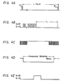
- the voltage V H (30 volts) is applied from the source 16 through the switching circuit 18 to the substrate 1 so as to discharge the signal charges accumulated in the signal charge accumulating region 3 in such a manner that an arbitrary number of the horizontal blanking periods, each being set at 63.5 microseconds, are successively selected.
- the switching circuit 18 is controlled by the control signal applied thereto from the terminal 19 so that the movable contact 18C engages the second fixed contact 18B.
- the voltage V H (30 volts) is applied to the substrate 1 at every horizontal blanking period to discharge the signal charges accumulated in the signal charge accumulating region 3 immediately before the exposure is started.
- the voltage V L (10 volts) is applied from the source 16 through the switching circuit 18 to the substrate 1 to accumulate signal charges in the signal charge accumulating region 3.
- Figure 4C shows a horizontal clock signal while Figure 4D shows a horizontal blanking signal, and Figure 4E shows the voltages to be applied to the substrate 1 within the horizontal blanking period.
- the exposure time t1 can be changed in a range between 1/60 and 1/0000 of a second by selecting the number of horizontal blanking periods for discharging the signal charges accumulated in the signal charge accumulating region 3, as shown in Figure 4B.
- the exposure time is controlled by changing the voltage applied to the substrate 1. Since the voltage V H is applied to the substrate 1 within the horizontal blanking period, even although a buffer amplifier and other devices forming the output section are caused to fluctuate by changing the voltage applied to the substrate 1, the reproduced image will not be influenced by the above change, so that it is possible to obtain reproduced images with a constant contrast.
- the above description relates to where the signal charges are discharged at every horizontal blanking period immediately before the exposure is started.
- modifications can be made dependent on the characteristics of a solid state imager device such as where the signal charges are discharged only once within the horizontal blanking period and immediately before the exposure is started or where some of the horizontal blanking periods before the exposure is started are selected to discharge the signal charges.
- the number of discharges can be selected in accordance with the characteristics of each solid state imager device.
Landscapes
- Transforming Light Signals Into Electric Signals (AREA)
- Solid State Image Pick-Up Elements (AREA)
Priority Applications (1)
| Application Number | Priority Date | Filing Date | Title |
|---|---|---|---|
| EP95202218A EP0683603B1 (de) | 1986-10-23 | 1987-10-22 | Elektronischer Verschluss für elektronische Kamera |
Applications Claiming Priority (4)
| Application Number | Priority Date | Filing Date | Title |
|---|---|---|---|
| JP61252375A JPH0759055B2 (ja) | 1986-10-23 | 1986-10-23 | 固体撮像装置 |
| JP252375/86 | 1986-10-23 | ||
| JP307474/86 | 1986-12-23 | ||
| JP61307474A JP2517882B2 (ja) | 1986-12-23 | 1986-12-23 | 固体撮像装置 |
Related Child Applications (2)
| Application Number | Title | Priority Date | Filing Date |
|---|---|---|---|
| EP95202218.4 Division-Into | 1987-10-22 | ||
| EP95202218A Division EP0683603B1 (de) | 1986-10-23 | 1987-10-22 | Elektronischer Verschluss für elektronische Kamera |
Publications (3)
| Publication Number | Publication Date |
|---|---|
| EP0265271A2 true EP0265271A2 (de) | 1988-04-27 |
| EP0265271A3 EP0265271A3 (de) | 1991-03-20 |
| EP0265271B1 EP0265271B1 (de) | 1996-04-17 |
Family
ID=26540691
Family Applications (2)
| Application Number | Title | Priority Date | Filing Date |
|---|---|---|---|
| EP87309365A Expired - Lifetime EP0265271B1 (de) | 1986-10-23 | 1987-10-22 | Elektronischer Verschluss für eine elektronische Kamera und Verfahren zur Verwendung eines CCD Bildsensors als elektronischer Verschluss für eine solche Kamera |
| EP95202218A Expired - Lifetime EP0683603B1 (de) | 1986-10-23 | 1987-10-22 | Elektronischer Verschluss für elektronische Kamera |
Family Applications After (1)
| Application Number | Title | Priority Date | Filing Date |
|---|---|---|---|
| EP95202218A Expired - Lifetime EP0683603B1 (de) | 1986-10-23 | 1987-10-22 | Elektronischer Verschluss für elektronische Kamera |
Country Status (5)
| Country | Link |
|---|---|
| US (1) | US4875100A (de) |
| EP (2) | EP0265271B1 (de) |
| DE (2) | DE3751775T2 (de) |
| HK (1) | HK1007833A1 (de) |
| SG (1) | SG74557A1 (de) |
Cited By (16)
| Publication number | Priority date | Publication date | Assignee | Title |
|---|---|---|---|---|
| EP0346905A3 (de) * | 1988-06-15 | 1991-01-02 | Nec Corporation | Regelungsverfahren der elektronischen Überblendung für eine zweidimensionale ladungsgekoppelte Anordnung |
| WO1991003839A1 (en) * | 1989-09-05 | 1991-03-21 | Eastman Kodak Company | Blooming control and reduced image lag in interline transfer ccd area image sensor |
| EP0353665A3 (de) * | 1988-07-30 | 1991-04-10 | Sony Corporation | CCD-Bilderzeugungsvorrichtung |
| GB2237472A (en) * | 1989-08-08 | 1991-05-01 | Asahi Optical Co Ltd | CCD imager with anti-blooming device |
| WO1991008590A1 (en) * | 1989-11-29 | 1991-06-13 | Eastman Kodak Company | Non-interlaced interline transfer ccd image sensing device with simplified electrode structure for each pixel |
| EP0410465A3 (en) * | 1989-07-28 | 1991-08-14 | Nec Corporation | Solid state image pickup device having photo-shield plate in contact with photo-electric converting region via schottky barrier |
| EP0372456A3 (de) * | 1988-12-07 | 1991-12-27 | Nec Corporation | CCD-Bildwandler mit senkrechtem Ueberlaufdrain |
| WO1992003850A3 (en) * | 1990-08-13 | 1992-05-14 | Eastman Kodak Co | Image sensor having transfer gate between the photodiode and the ccd element |
| WO1992013361A1 (en) * | 1991-01-22 | 1992-08-06 | Eastman Kodak Company | Blooming control and reduced image lag in interline transfer ccd area image sensor |
| EP0403939A3 (de) * | 1989-06-20 | 1992-08-12 | Sanyo Electric Co., Ltd. | Ansteuerverfahren eines Festkörper-Bildaufnehmers |
| EP0502521A1 (de) * | 1991-03-06 | 1992-09-09 | Matsushita Electronics Corporation | Festkörperbildaufnahmeanordnung und deren Herstellungsprozess |
| EP0519443A1 (de) * | 1991-06-21 | 1992-12-23 | Sony Corporation | Ladungsgekoppelter Bildsensor |
| EP0572137A1 (de) * | 1992-05-27 | 1993-12-01 | Loral Fairchild Corporation | Ladungsabschöpfung und variable Integrationszeit in einer Bildebenenmatrixanordnung |
| EP1143522A3 (de) * | 2000-04-06 | 2008-03-26 | Nec Corporation | Ladungsgekoppelte Anordnung und Verfahren zu ihrer Herstellung |
| RU2674646C1 (ru) * | 2018-03-12 | 2018-12-12 | Вячеслав Михайлович Смелков | Способ управления поэлементным переносом зарядовых пакетов в матричном фотоприёмнике на ПЗС |
| RU2675245C1 (ru) * | 2018-02-26 | 2018-12-18 | Вячеслав Михайлович Смелков | Устройство "кольцевого" фотоприёмника для панорамного телевизионно-компьютерного сканирования цветного изображения |
Families Citing this family (26)
| Publication number | Priority date | Publication date | Assignee | Title |
|---|---|---|---|---|
| JP2727584B2 (ja) * | 1988-09-20 | 1998-03-11 | ソニー株式会社 | 固体撮像装置 |
| DE3839513A1 (de) * | 1988-11-23 | 1990-05-31 | Messerschmitt Boelkow Blohm | Bildsensor |
| US5017004A (en) * | 1988-12-22 | 1991-05-21 | Westinghouse Electric Corp. | Multifunction electro-optical system test tool |
| US5198890A (en) * | 1989-03-30 | 1993-03-30 | Canon Kabushiki Kaisha | White balance correcting device for an image sensing |
| JPH02309877A (ja) * | 1989-05-25 | 1990-12-25 | Sony Corp | 固体撮像装置 |
| JPH03120979A (ja) * | 1989-10-04 | 1991-05-23 | Fuji Photo Film Co Ltd | 撮像装置 |
| US5162913A (en) * | 1990-02-26 | 1992-11-10 | Medical Concepts, Inc. | Apparatus for modulating the output of a ccd camera |
| JP3097121B2 (ja) * | 1990-09-27 | 2000-10-10 | ソニー株式会社 | 電荷/電圧変換効率の測定方法 |
| KR930008527B1 (ko) * | 1990-10-13 | 1993-09-09 | 금성일렉트론 주식회사 | Npn형 vccd 구조의 고체촬상 소자 |
| JPH04170175A (ja) * | 1990-11-02 | 1992-06-17 | Canon Inc | 固体撮像素子の駆動装置 |
| US5576762A (en) * | 1990-11-07 | 1996-11-19 | Canon Kabushiki Kaisha | Solid-state image pickup device |
| US5528291A (en) * | 1991-09-25 | 1996-06-18 | Fuji Photo Film Co., Ltd. | CCD image pickup device and method of driving which maintains sensitivity regardless of the operating mode |
| KR970007711B1 (ko) * | 1993-05-18 | 1997-05-15 | 삼성전자 주식회사 | 오버-플로우 드레인(ofd)구조를 가지는 전하결합소자형 고체촬상장치 |
| JP3015246B2 (ja) * | 1993-10-08 | 2000-03-06 | シャープ株式会社 | 固体撮像装置 |
| US5444280A (en) * | 1993-12-20 | 1995-08-22 | Scientific Imaging Technologies, Inc. | Photodetector comprising avalanche photosensing layer and interline CCD readout layer |
| US5598210A (en) * | 1995-02-15 | 1997-01-28 | Eastman Kodak Company | On chip driver for electric shuttering |
| JPH0997894A (ja) * | 1995-09-29 | 1997-04-08 | Sanyo Electric Co Ltd | 固体撮像素子の駆動方法 |
| JP3598648B2 (ja) * | 1996-04-02 | 2004-12-08 | ソニー株式会社 | 電荷転送素子及び電荷転送素子の駆動方法 |
| CN1081422C (zh) * | 1997-11-13 | 2002-03-20 | 点晶科技股份有限公司 | 具有电子快门的影像感应器 |
| CN100510933C (zh) | 1999-08-17 | 2009-07-08 | 应用视像系统有限公司 | 改善了动态范围的视频摄像机、记录系统和记录方法 |
| CN1329728C (zh) * | 2001-05-21 | 2007-08-01 | 派拉斯科技术公司 | 一种用于在自动化过程控制工件检查应用中提供热红外成像快照动作的装置及方法 |
| US6677999B2 (en) | 2001-07-09 | 2004-01-13 | Hewlett-Packard Development Company, L.P. | Non-polarizing LCD shutter |
| US7106377B2 (en) * | 2001-07-25 | 2006-09-12 | Hewlett-Packard Development Company, L.P. | Image capturing device capable of single pixel exposure duration control |
| US20030020958A1 (en) * | 2001-07-30 | 2003-01-30 | Bean Heather Noel | Non-polarizing shutter/CCD module |
| US20050212936A1 (en) * | 2004-03-25 | 2005-09-29 | Eastman Kodak Company | Extended dynamic range image sensor with fixed pattern noise reduction |
| KR100761048B1 (ko) | 2006-08-24 | 2007-09-21 | 주식회사 쎄이미지 | 고감도 시시디 이미지센서 및 그 제조방법 |
Family Cites Families (11)
| Publication number | Priority date | Publication date | Assignee | Title |
|---|---|---|---|---|
| US3934161A (en) * | 1974-04-29 | 1976-01-20 | Texas Instruments Incorporated | Electronic shutter for a charge-coupled imager |
| DE3138240A1 (de) * | 1981-09-25 | 1983-04-07 | Siemens AG, 1000 Berlin und 8000 München | Zweidimensionaler halbleiter-bildsensor mit steuerung oder regelung der integrationszeit |
| JPS58142570A (ja) * | 1982-02-19 | 1983-08-24 | Sony Corp | 固体撮像装置 |
| JPS5919480A (ja) * | 1982-07-26 | 1984-01-31 | Olympus Optical Co Ltd | 固体撮像装置 |
| JPS59108463A (ja) * | 1982-12-14 | 1984-06-22 | Olympus Optical Co Ltd | 固体撮像装置 |
| JPS59153381A (ja) * | 1983-02-22 | 1984-09-01 | Junichi Nishizawa | 2次元固体撮像装置 |
| JPS6020687A (ja) * | 1983-07-15 | 1985-02-01 | Nippon Kogaku Kk <Nikon> | 電子スチルカメラ |
| JPH0824351B2 (ja) * | 1984-04-27 | 1996-03-06 | オリンパス光学工業株式会社 | 固体撮像装置 |
| JPS6157181A (ja) * | 1984-08-28 | 1986-03-24 | Sharp Corp | 固体撮像装置 |
| US4743778A (en) * | 1985-03-25 | 1988-05-10 | Nippon Kogaku K. K. | Solid-state area imaging device having interline transfer CCD |
| NL8602091A (nl) * | 1986-08-18 | 1988-03-16 | Philips Nv | Beeldopneeminrichting uitgevoerd met een vaste-stof beeldopnemer en een elektronische sluiter. |
-
1987
- 1987-10-21 US US07/110,844 patent/US4875100A/en not_active Expired - Lifetime
- 1987-10-22 SG SG1996008391A patent/SG74557A1/en unknown
- 1987-10-22 DE DE3751775T patent/DE3751775T2/de not_active Expired - Lifetime
- 1987-10-22 EP EP87309365A patent/EP0265271B1/de not_active Expired - Lifetime
- 1987-10-22 DE DE3752305T patent/DE3752305T2/de not_active Expired - Lifetime
- 1987-10-22 EP EP95202218A patent/EP0683603B1/de not_active Expired - Lifetime
-
1998
- 1998-06-26 HK HK98107004A patent/HK1007833A1/en not_active IP Right Cessation
Cited By (21)
| Publication number | Priority date | Publication date | Assignee | Title |
|---|---|---|---|---|
| EP0346905A3 (de) * | 1988-06-15 | 1991-01-02 | Nec Corporation | Regelungsverfahren der elektronischen Überblendung für eine zweidimensionale ladungsgekoppelte Anordnung |
| EP0353665A3 (de) * | 1988-07-30 | 1991-04-10 | Sony Corporation | CCD-Bilderzeugungsvorrichtung |
| EP0372456A3 (de) * | 1988-12-07 | 1991-12-27 | Nec Corporation | CCD-Bildwandler mit senkrechtem Ueberlaufdrain |
| EP0403939A3 (de) * | 1989-06-20 | 1992-08-12 | Sanyo Electric Co., Ltd. | Ansteuerverfahren eines Festkörper-Bildaufnehmers |
| EP0410465A3 (en) * | 1989-07-28 | 1991-08-14 | Nec Corporation | Solid state image pickup device having photo-shield plate in contact with photo-electric converting region via schottky barrier |
| US5339162A (en) * | 1989-08-08 | 1994-08-16 | Asahi Kogaku Kogyo Kabushiki Kaisha | Driving apparatus of image pick-up device for preventing leakage of accumulated electrical charges |
| GB2237472A (en) * | 1989-08-08 | 1991-05-01 | Asahi Optical Co Ltd | CCD imager with anti-blooming device |
| USRE36812E (en) * | 1989-08-08 | 2000-08-08 | Asahi Kogaku Kogyo Kabushiki Kaisha | Driving apparatus of image pick-up device for preventing leakage of accumulated electrical charges |
| GB2237472B (en) * | 1989-08-08 | 1994-01-26 | Asahi Optical Co Ltd | Image pick-up device driving aparatus |
| WO1991003839A1 (en) * | 1989-09-05 | 1991-03-21 | Eastman Kodak Company | Blooming control and reduced image lag in interline transfer ccd area image sensor |
| WO1991008590A1 (en) * | 1989-11-29 | 1991-06-13 | Eastman Kodak Company | Non-interlaced interline transfer ccd image sensing device with simplified electrode structure for each pixel |
| WO1992003850A3 (en) * | 1990-08-13 | 1992-05-14 | Eastman Kodak Co | Image sensor having transfer gate between the photodiode and the ccd element |
| WO1992013361A1 (en) * | 1991-01-22 | 1992-08-06 | Eastman Kodak Company | Blooming control and reduced image lag in interline transfer ccd area image sensor |
| EP0502521A1 (de) * | 1991-03-06 | 1992-09-09 | Matsushita Electronics Corporation | Festkörperbildaufnahmeanordnung und deren Herstellungsprozess |
| US5424775A (en) * | 1991-03-06 | 1995-06-13 | Matsushita Electronics Corporation | Solid-state image pickup device and method of manufacturing the same |
| EP0519443A1 (de) * | 1991-06-21 | 1992-12-23 | Sony Corporation | Ladungsgekoppelter Bildsensor |
| US5286988A (en) * | 1991-06-21 | 1994-02-15 | Sony Corporation | Charge coupled device image sensor |
| EP0572137A1 (de) * | 1992-05-27 | 1993-12-01 | Loral Fairchild Corporation | Ladungsabschöpfung und variable Integrationszeit in einer Bildebenenmatrixanordnung |
| EP1143522A3 (de) * | 2000-04-06 | 2008-03-26 | Nec Corporation | Ladungsgekoppelte Anordnung und Verfahren zu ihrer Herstellung |
| RU2675245C1 (ru) * | 2018-02-26 | 2018-12-18 | Вячеслав Михайлович Смелков | Устройство "кольцевого" фотоприёмника для панорамного телевизионно-компьютерного сканирования цветного изображения |
| RU2674646C1 (ru) * | 2018-03-12 | 2018-12-12 | Вячеслав Михайлович Смелков | Способ управления поэлементным переносом зарядовых пакетов в матричном фотоприёмнике на ПЗС |
Also Published As
| Publication number | Publication date |
|---|---|
| US4875100A (en) | 1989-10-17 |
| DE3752305D1 (de) | 2000-01-27 |
| EP0265271B1 (de) | 1996-04-17 |
| EP0683603A3 (de) | 1995-12-13 |
| EP0265271A3 (de) | 1991-03-20 |
| SG74557A1 (en) | 2000-08-22 |
| HK1013568A1 (en) | 1999-08-27 |
| EP0683603B1 (de) | 1999-12-22 |
| EP0683603A2 (de) | 1995-11-22 |
| DE3752305T2 (de) | 2000-06-21 |
| DE3751775T2 (de) | 1996-10-10 |
| DE3751775D1 (de) | 1996-05-23 |
| HK1007833A1 (en) | 1999-04-23 |
Similar Documents
| Publication | Publication Date | Title |
|---|---|---|
| EP0265271B1 (de) | Elektronischer Verschluss für eine elektronische Kamera und Verfahren zur Verwendung eines CCD Bildsensors als elektronischer Verschluss für eine solche Kamera | |
| HK1007833B (en) | Electronic shutter for an electronic camera and method of utilizing a ccd image sensor as electronic shutter for such a camera | |
| US3931465A (en) | Blooming control for charge coupled imager | |
| US4835404A (en) | Photoelectric converting apparatus with a switching circuit and a resetting circuit for reading and resetting a plurality of lines sensors | |
| EP0265925B1 (de) | Elektronische Stehbildkamera | |
| US5270531A (en) | Source follower circuit for image sensor | |
| US4589027A (en) | Solid state image sensor | |
| US4845566A (en) | Solid-state image pickup apparatus having controllable means for eliminating surplus charge | |
| EP0403939B1 (de) | Ansteuerverfahren eines Festkörper-Bildaufnehmers | |
| EP0247503B1 (de) | Steuerverfahren für einen Festkörperbildgeber | |
| US5631705A (en) | Video camera having circuit for setting exposure compensation value | |
| US4856033A (en) | Solid state imager device with exposure control with noise reduction | |
| EP0088134B1 (de) | Integrierte bildaufnahmevorrichtung | |
| US4603343A (en) | Solid state image sensor applied with differing read-out gate voltages | |
| EP0621726A1 (de) | Verfahren und Gerät für eine Festkörper-Bildaufnahme-Vorrichtung | |
| JPH0759055B2 (ja) | 固体撮像装置 | |
| US5831675A (en) | Solid state imaging device | |
| KR100218771B1 (ko) | 고체촬상소자 | |
| HK1013568B (en) | Electronic shutter for electronic camrea | |
| KR970007895B1 (ko) | 고체촬상장치 및 노광시간제어방법 | |
| US4845568A (en) | Image pickup apparatus for selectively storing electrical signals | |
| JP2565247B2 (ja) | 固体撮像装置及びビデオカメラの露光時間制御方法 | |
| JPH0446504B2 (de) | ||
| EP0100368B1 (de) | Halbleiter-bildaufzeichnungsvorrichtung | |
| EP0055530B1 (de) | Halbleiterbildsensor |
Legal Events
| Date | Code | Title | Description |
|---|---|---|---|
| PUAI | Public reference made under article 153(3) epc to a published international application that has entered the european phase |
Free format text: ORIGINAL CODE: 0009012 |
|
| AK | Designated contracting states |
Kind code of ref document: A2 Designated state(s): DE FR GB NL |
|
| PUAL | Search report despatched |
Free format text: ORIGINAL CODE: 0009013 |
|
| AK | Designated contracting states |
Kind code of ref document: A3 Designated state(s): DE FR GB NL |
|
| 17P | Request for examination filed |
Effective date: 19910809 |
|
| 17Q | First examination report despatched |
Effective date: 19920701 |
|
| GRAH | Despatch of communication of intention to grant a patent |
Free format text: ORIGINAL CODE: EPIDOS IGRA |
|
| GRAA | (expected) grant |
Free format text: ORIGINAL CODE: 0009210 |
|
| AK | Designated contracting states |
Kind code of ref document: B1 Designated state(s): DE FR GB NL |
|
| XX | Miscellaneous (additional remarks) |
Free format text: TEILANMELDUNG 95202218.4 EINGEREICHT AM 16/08/95. |
|
| REF | Corresponds to: |
Ref document number: 3751775 Country of ref document: DE Date of ref document: 19960523 |
|
| ET | Fr: translation filed | ||
| PLBE | No opposition filed within time limit |
Free format text: ORIGINAL CODE: 0009261 |
|
| STAA | Information on the status of an ep patent application or granted ep patent |
Free format text: STATUS: NO OPPOSITION FILED WITHIN TIME LIMIT |
|
| 26N | No opposition filed | ||
| REG | Reference to a national code |
Ref country code: GB Ref legal event code: IF02 |
|
| PGFP | Annual fee paid to national office [announced via postgrant information from national office to epo] |
Ref country code: NL Payment date: 20061003 Year of fee payment: 20 |
|
| PGFP | Annual fee paid to national office [announced via postgrant information from national office to epo] |
Ref country code: GB Payment date: 20061018 Year of fee payment: 20 |
|
| PGFP | Annual fee paid to national office [announced via postgrant information from national office to epo] |
Ref country code: DE Payment date: 20061019 Year of fee payment: 20 |
|
| REG | Reference to a national code |
Ref country code: GB Ref legal event code: PE20 |
|
| NLV7 | Nl: ceased due to reaching the maximum lifetime of a patent |
Effective date: 20071022 |
|
| PG25 | Lapsed in a contracting state [announced via postgrant information from national office to epo] |
Ref country code: NL Free format text: LAPSE BECAUSE OF EXPIRATION OF PROTECTION Effective date: 20071022 |
|
| PG25 | Lapsed in a contracting state [announced via postgrant information from national office to epo] |
Ref country code: GB Free format text: LAPSE BECAUSE OF EXPIRATION OF PROTECTION Effective date: 20071021 |
|
| PGFP | Annual fee paid to national office [announced via postgrant information from national office to epo] |
Ref country code: FR Payment date: 20061010 Year of fee payment: 20 |