EP0265237A2 - Dispositif de commande pour éclairage à décharge gazeuse haute-intensité - Google Patents
Dispositif de commande pour éclairage à décharge gazeuse haute-intensité Download PDFInfo
- Publication number
- EP0265237A2 EP0265237A2 EP87309290A EP87309290A EP0265237A2 EP 0265237 A2 EP0265237 A2 EP 0265237A2 EP 87309290 A EP87309290 A EP 87309290A EP 87309290 A EP87309290 A EP 87309290A EP 0265237 A2 EP0265237 A2 EP 0265237A2
- Authority
- EP
- European Patent Office
- Prior art keywords
- circuit
- control gear
- lamp
- mark
- capacitor
- Prior art date
- Legal status (The legal status is an assumption and is not a legal conclusion. Google has not performed a legal analysis and makes no representation as to the accuracy of the status listed.)
- Withdrawn
Links
Images


Classifications
-
- H—ELECTRICITY
- H05—ELECTRIC TECHNIQUES NOT OTHERWISE PROVIDED FOR
- H05B—ELECTRIC HEATING; ELECTRIC LIGHT SOURCES NOT OTHERWISE PROVIDED FOR; CIRCUIT ARRANGEMENTS FOR ELECTRIC LIGHT SOURCES, IN GENERAL
- H05B41/00—Circuit arrangements or apparatus for igniting or operating discharge lamps
- H05B41/14—Circuit arrangements
- H05B41/36—Controlling
- H05B41/38—Controlling the intensity of light
- H05B41/39—Controlling the intensity of light continuously
- H05B41/392—Controlling the intensity of light continuously using semiconductor devices, e.g. thyristor
-
- H—ELECTRICITY
- H05—ELECTRIC TECHNIQUES NOT OTHERWISE PROVIDED FOR
- H05B—ELECTRIC HEATING; ELECTRIC LIGHT SOURCES NOT OTHERWISE PROVIDED FOR; CIRCUIT ARRANGEMENTS FOR ELECTRIC LIGHT SOURCES, IN GENERAL
- H05B41/00—Circuit arrangements or apparatus for igniting or operating discharge lamps
- H05B41/14—Circuit arrangements
- H05B41/26—Circuit arrangements in which the lamp is fed by power derived from dc by means of a converter, e.g. by high-voltage dc
- H05B41/28—Circuit arrangements in which the lamp is fed by power derived from dc by means of a converter, e.g. by high-voltage dc using static converters
- H05B41/288—Circuit arrangements in which the lamp is fed by power derived from dc by means of a converter, e.g. by high-voltage dc using static converters with semiconductor devices and specially adapted for lamps without preheating electrodes, e.g. for high-intensity discharge lamps, high-pressure mercury or sodium lamps or low-pressure sodium lamps
- H05B41/292—Arrangements for protecting lamps or circuits against abnormal operating conditions
- H05B41/2921—Arrangements for protecting lamps or circuits against abnormal operating conditions for protecting the circuit against abnormal operating conditions
- H05B41/2925—Arrangements for protecting lamps or circuits against abnormal operating conditions for protecting the circuit against abnormal operating conditions against abnormal lamp operating conditions
-
- H—ELECTRICITY
- H05—ELECTRIC TECHNIQUES NOT OTHERWISE PROVIDED FOR
- H05B—ELECTRIC HEATING; ELECTRIC LIGHT SOURCES NOT OTHERWISE PROVIDED FOR; CIRCUIT ARRANGEMENTS FOR ELECTRIC LIGHT SOURCES, IN GENERAL
- H05B41/00—Circuit arrangements or apparatus for igniting or operating discharge lamps
- H05B41/14—Circuit arrangements
- H05B41/36—Controlling
- H05B41/38—Controlling the intensity of light
- H05B41/39—Controlling the intensity of light continuously
- H05B41/392—Controlling the intensity of light continuously using semiconductor devices, e.g. thyristor
- H05B41/3921—Controlling the intensity of light continuously using semiconductor devices, e.g. thyristor with possibility of light intensity variations
- H05B41/3927—Controlling the intensity of light continuously using semiconductor devices, e.g. thyristor with possibility of light intensity variations by pulse width modulation
- H05B41/3928—Controlling the intensity of light continuously using semiconductor devices, e.g. thyristor with possibility of light intensity variations by pulse width modulation for high-pressure lamps, e.g. high-intensity discharge lamps, high-pressure mercury or sodium lamps
Definitions
- This invention relates to control gear for high intensity gas discharge lighting.
- a control gear for a high intensity gas discharge lighting tube comprising an oscillator, a high speed switching element driven by said oscillator, a transformer having its primary winding connected in a series resonant circuit tuned to the frequency of the oscillator and controlled by the switching element and means for connecting the secondary winding of the transformer to the lighting tube.
- the series resonant circuit including the primary winding of the transformer ensures that the switching transients normally obtained from the use of conventional switch mode power supplies are avoided, thereby avoiding mains waveform distortion and radio frequency interference.
- said switching element is connected across a capacitor which forms a part of said series resonant circuit.
- the switch device is a gate turn-off thyristor.
- a drive circuit is interposed between the switching device and the oscillator and includes means for controlling the mark-space ratio of the drive signals applied to the switching device.
- the mark-space ratio control preferably includes means to set the mark-space ratio at about unity initial so as to provide a very high amplitude signal from the series tuned circuit, whereby a high voltage is provided across the lamp for causing initial ionisation of the gas therein.
- Such mark-space ratio control may include a feedback circuit connected to the transformer secondary winding and sensitive to the power supplied to the lighting tube.
- the transformer preferably comprises a core which fully contains the primary and secondary windings.
- the core may comprise a sleeve part and a spool-shaped part fitted within the sleeve part, both parts being formed of bonded iron powder.
- control gear shown makes use of a switching device in the form of a gate turn-off thyristor 10 to control current in the primary winding of a transformer, the primary winding of which is connected in a series resonant circuit 11 across a rectified mains supply provided by a main power rectifier 12.
- the secondary winding of the transformer has the lamp 13 connected across it and there is a power detector circuit 14 connected in circuit with the lamp 13.
- a driver circuit 15 for the GTO 10 is supplied by two switch mode power supply units 16, 17 providing +15V d.c. and -10V d.c. respectively.
- Another 15V supply 18 derives power directly from the mains input and provides current to an oscillator 19 which switches the input to the driver 15 through the intermediary of a comparator circuit 20 providing a variable mark-space ratio to the driver 15.
- the detector 14 and a feedback circuit 21 are arranged to vary the reference voltage supplied to the comparator 20 so as, in use, to ensure that the lamp 13 is driven at a predetermined power level.
- a start-up and control circuit 22 also controls the comparator 20 via the circuit 21 as will be explained in more detail hereinafter.
- the main transformer which provides current to the lamp includes a core moulded from resin-bonded iron powder.
- resin-bonded iron powder Preferably hydrogen-reduced iron powder in a conventional polyester resin is used, the iron powder representing about 80% of the weight of the mixture.
- the transformer core basically comprises a main moulding consisting of an outer sleeve 30 a disc and a spigot 31.
- the moulded part is dip-varnished to avoid the need for an insulating spool and the primary winding 33 and the secondary windings of the transformer are wound and then dropped on to the spigot.
- the core is completed by a layer 32 of the iron containing resin formed in situ.
- the secondary winding 34 is wound on the outside of the primary winding.
- One suitable transformer has an outer diameter of about 40mm, a length of about 30mm, a primary winding of 80 turns and a secondary winding of 180 turns.
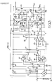
- the power supply circuits of Figure 1 are shown in detail in Figure 3.
- the power rectifier 12 is a bridge rectifier which provides an output voltage of about 330V between a supply rail 8 and a return rail 9.
- a surge prevention circuit consisting of a resistor R1, a voltage dependent resistor VDR and a capacitor C1 in parallel is connected across this output.
- the 15 volt supply 18 consists simply of a coupling capacitor C2, a 15 volt zener diode ZD1, a diode D1 and a capacitor C3.
- the two switch mode power supplies 16 and 17 are driven by a common oscillator comprising a single CMOS NAND gate 40 with its two inputs connected together, a feedback resistor R2 and a capacitor C3 connecting these inputs to rail 9.
- An npn transistor Q1 connected as a voltage follower and having an emitter load resistor R, buffers the voltage signal on the capacitor C4 and provides the output of the oscillator.
- Comparator A1 has its input terminals connected by respective resistors R3, R4 to the oscillator output.
- the non-inverting input is connected by a capacitor C5 to rail 9 and is also connected to the collector of an npn transistor Q2 which has its emitter connected to rail 9 by a resistor R5.
- the output of comparator A1 is connected by a pull-up resistor R6 to the cathode of diode D1 and is also connected to the base of an npn transistor Q3, which has its emitter connected to rail 9.
- the transistor Q3 has a collector load resistor R7 and its collector is also coupled by a capacitor C6 to the base of an npn resistor Q4 which has its emitter connected to rail 9.
- a resistor R8 connects the base of transistor Q4 to rail 9 and a further resistor R9 connects the collector thereof to the 330V d.c. supply conductor.
- An npn Darlington pair Q5 has its common collector connected to the 330V d.c. supply, its base connected to the collector of transistor Q4 and its emitter connected via a capacitor C7 and resistor R10, in parallel, to one end of the primary winding of a transformer 41, the other end of this primary winding being connected to rail 9.
- a resistor R11 connects the emitter of the Darlington pair Q5 to the collector of the transistor Q4.
- the secondary winding of the transformer 41 has one end connected to rail 9 and the other end connected to the anode of a diode D2.
- a 15V zener diode ZD2 has its cathode connected to the cathode of diode D2 and its anode connected to rail 9 via two resistors R12, R13 in series and the junction of these resistors is connected to the base of the Q2 to provide voltage feedback around the power supply.
- a reservoir capacitor C8 is connected between the cathode of diode D2 and rail 9.
- the feedback circuit provided by the zener diode ZD2 and the transistor Q2 operates to maintain the mark-space ratio of the output of the comparator A1 at a level sufficient to provide the required output voltage at the cathode of diode D2. Any increase in load current which will cause the voltage on capacitor C8 to start to fall will be automatically adjusted by a corresponding increase in the mark to space ratio resulting from the increased conduction of the transistor Q2.
- the -10V switch mode power supply is of similar design and includes components R ⁇ 3 to R ⁇ 11, C ⁇ 5 to C ⁇ 8, Q ⁇ 2 to Q ⁇ 5, 41 ⁇ , and D ⁇ 2 corresponding precisely to the correspondingly referenced components in the +15V d.c. switch mode power supply, except that the diode D ⁇ 2 is reversed to provide a negative voltage on capacitor C ⁇ 8.
- the feedback circuit in this case includes a zener diode ZD ⁇ 2 which has it anode connected to the anode of the diode D ⁇ 2 and its cathode connected by two resistors R ⁇ 12, R ⁇ 13 in series to the cathode of diode D2.
- the zener diode ZD ⁇ 2 has a 24V breakdown voltage.
- a pnp transistor Q6 has its emitter connected to the cathode of diode D2 and its collector connected by a resistor R14 and a capacitor C9, in parallel, to rail 9. Two resistors R15, R16 are connected in series across the capacitor C9 and their junction is connected to the base of transistor Q ⁇ 2. This arrangement provides for the mark-space ratio of the output of the comparator to be increased if the voltage at the anode of diode D ⁇ 2 tends to rise as a result of increased current being drawn.
- Figure 3 also shows a diode D3 which connects the output of the 15V d.c. switch mode power supply to the cathode of D1, so that the simple zener diode shunt regulator 15V d.c. supply is only needed at start up or if the switch mode power supply output voltage falls during use for any reason.
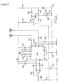
- FIG 4 shows in detail the lamp circuit, the series resonant circuit, the driver for the GTO and the control for the driver shown in Figure 1 and described in general terms above.
- the GTO 10 has its cathode connected to rail 9 and its anode connected via a series circuit consisting of the primary winding of a GTO current detector transformer 50, an inductor 51 and the primary winding 33 of the main transformer.
- the inductor 51 may be of similar design to the main transformer, except that it is also formed of resin bonded iron powder. It may typically have an inductance of 1.3mH.
- the interconnection of the inductor 51 and the primary winding 33 is connected by a capacitor C10, typically of about 10nF capacitance, to rail 9.
- the anode of the GTO 10 is connected by another capacitor C11, typically of about 1nF capacitance, to rail 9.
- a diode D4 has its cathode connected to anode of GTO 10 and its anode connected to rail 9 and a snubber circuit, consisting of a capacitor C12 in series with the parallel combination of a resistor R17 and a diode D5 also connects the anode of GTO 10 to rail 9.
- the dominant components which determine the resonant frequency of the circuit described above are the inductor 51 and the capacitor C1.
- the oscillator 19 of Figure 1 is of similar construction to that used to drive the power supplies, that is to say it includes a single CMOS NAND gate with a feedback resistor (R18 and R ⁇ 18 in series) and a capacitor C13 connecting the gate input to rail 9.
- the comparator 20 includes an integrated circuit voltage comparator A3 which has its inputs connected by resistors R19 and R20 respectively to the oscillator output.
- the non-inverting input of comparator A3 is connected to a reference voltage source, such as the slider of a potentiometer R21 connected between the +15V and -10V d.c. supply rails.
- a capacitor C14 connects the inverting input of comparator A3 to rail 9.
- the output of amplifier A3 is connected by a pull-up resistor R22 to the +15V supply rail and by a capacitor C15 to the base of an npn transistor Q7 which has its emitter connected to the -10V supply rail.
- a resistor R23 connects the base of transistor Q7 to the +15V supply rail and a diode D6 has its cathode connected to the base of transistor Q7 and its anode connected to the -10V supply rail.
- a resistor R24 connects the collector of the transistor Q7 to the +15V supply rail.
- the collector of transistor Q7 is connected to drive a push-pull output stage of the driver circuit.
- This output stage comprises an npn Darlington pair Q8 and a pnp Darlington pair Q9 with their emitters connected together and to the GTO gate.
- the collectors of Darlington pair Q8 are connected by a resistor R25 and a capacitor C16, in parallel, to the +15V rail and those of the Darlington pair Q9 are connected directly to the -10V rail.
- the bases of the two Darlington pairs are connected by respective resistors R26, R27 to the collector of transistor Q7.
- the output of the oscillator 19 is a triangular wave of frequency determined by the values of resistor R18 and capacitor C13. Ignoring for the moment a diode D7 which is connected to the inverting input of comparator A3, the output of A3 is low whenever the oscillator output voltage is less than the reference voltage on the slider of potentiometer R21 and goes high while the oscillator output is higher than this reference voltage. Resistor R23 biases transistor Q7 on, but transistor Q7 is turned off when the output of the comparator A3 goes low. This causes the GTO 10 to be turned on.
- the variable resistor R ⁇ 18 is adjusted to set the oscillator frequency to be substantially the same as the resonant frequency of the series resonant circuit and the resistor R21 is set to provide the maximum required mark to space ratio of the circuit.
- the diode D7 is connected to the feedback and control circuit and can only cause the reference voltage at the inverting input of comparator A3 to be reduced, thereby reducing the mark-space ratio and reducing the power transferred to the lamp.
- the comparator A3 can, in fact be completely inhibited by drawing sufficient current via the diode D7 as will be hereinafter explained.
- the secondary winding 34 of the main transformer has a capacitor C17 connected across it.
- the lamp is connected in series with the primary winding of a current sensing transformer 52 across the secondary winding 34.
- a voltage sensing circuit comprising a transformer 54 and a resistor R28, the resistor being in series with the primary winding of the transformer 54.
- the secondary winding of each of the transformers 50, 53 and 54 is connected to rail 9 at one end, the other end (50 a , 52 a , 53 a ) being connected to the feedback and control circuits shown in detail in Figures 5 and 6.
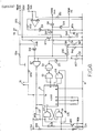
- the circuit includes a four quadrant analog multiplier integrated circuit 60.
- the outputs of the two transformers 52 and 53 are connected via respective resistors R30, R31, to the +X and +Y inputs of the circuit 60, these inputs being connected to rail 9 via respective resistors R32, R33.
- the -X and -Y inputs of circuit 60 are connected to rail 9.
- the supply input (pin 1) of circuit 60 is connected by a resistor R34 to the +15V supply and pins 3 and 13 thereof are connected together and connected to rail 9 by a resistor R35.
- Pins 5 and 6 are interconnected by a resistor R36 and pins 10 and 11 are interconnected by a resistor R37 (as is conventional).
- Pin 7 is connected to the -10V supply.
- the output of circuit 60 appears across its pins 2 and 14 and these pins are connected by respective pull-up resistors R38, R39 to the +15V supply and by respective resistors R40 and R41 to the respective non-inverting and inverting inputs of an operational amplifier A4 connected as a differential amplifier with a gain of about 50.
- a feedback resistor R42 connects the output of amplifier A4 to its inverting input and a resistor R43 connects the non-inverting input of amplifier A4 to rail 9.
- the output of amplifier A4 is connected by a resistor R44 to the anode of a diode D8 (see Figure 6) which is also connected to rail 9 by a capacitor C18.
- the output of amplifier A4 is proportional to the instantaneous value of the power consumed by the lamp 13 as the multiplier circuit multiplies signals represent the lamp voltage and current respectively.
- Resistor R44 and capacitor C18 effectively remove the a.c. components of the signal at the output of amplifier A4 and leave a d.c. signal representing the "average" power consumption of the lamp.
- the resistor 44 and capacitor C18 have a time constant of about 1mS.
- the cathode of diode D8 is connected to the cathode of a 6.8V zener diode ZD2 which has its anode connected by two resistors R45, R46 in series to rail 9.
- the interconnection of these two resistors is connected to the base of an npn transistor Q10 which has its emitter connected to rail 9 by a resistor R47.
- the collector of transistor Q10 is connected by a resistor R48 to the +15V supply and by a capacitor C19 to rail 9.
- the resistor R48 provides a charging circuit for the capacitor C19 which circuit has a time constant of about 2 seconds.
- the resistor R47 and transistor Q10 provide a discharge path with a time constant of about 0.2 seconds.
- An npn transistor Q11 is provided as a voltage follower to buffer the voltage on the capacitor C10.
- the emitter of transistor Q11 is connected by a resistor R49 to rail 9 and its collector is connected directly to the +15V supply.
- the emitter of transistor Q11 is connected directly to the cathode of the diode D7.
- the circuit described above constitutes the main control loop for regulating the lamp power. It will be understood that any tendency for the lamp power to increase will result in the voltage on capacitor C18 rising. This will turn transistor Q10 on causing the voltage on capacitor C19 to start to fall, which in turn will reduce the mark-space ratio of the output of the amplifer A3 and will thereby reduce the power consumed. Conversely, any tendency for the lamp power to decrease will result in the charge on capacitor C19 increasing so that the mark-space ratio is increased. It should be noted that increase of the mark-space ratio is allowed to occur at a slower rate than decrease thereof.
- the output of the transformer 50 is applied via a resistor R50 to the inverting input terminal of an operational amplifier A5 and by a resistor R51 to rail 9.
- a feedback resistor R52 connects the output of amplifier A5 to its inverting input.
- the output of amplifier A5 is connected to the anode of a diode D9, the cathode of which is connected by a resistor R53 to one terminal of a capacitor C20 the other terminal of which is connected to rail 9.
- a resistor R54 is connected across capacitor C20.
- the resistor R53 provides a charging path for capacitor C20 having a time-constant of about 0.2mS, whereas the resistor R54 provides a discharge path having a time constant of about 10mS, so that the capacitor C20 operates as a peak store and the voltage across it corresponds to the peaks in the current waveform in the inductor 51.
- a diode D10 connects the first-mentioned terminal of the capacitor C20 to the cathode of zener diode ZD2 so that, should the peak current referred to rise above a predetermined level, such that the voltage on capacitor C20 is higher than reverse breakdown voltage of zener diode ZD2, the mark-space ratio will be overridingly reduced to protect the GTO from damage by an excessive current level.
- the circuit shown in the left hand half of Figure 6 controls starting of the system.
- This includes a push-button switch 70 which connects the +15V supply to the cathode of zener diode ZD2 via a resistor R. Closure of this switch forces the transistor Q10 to turn on, discharging capacitor C19 and turning the lamp driver circuit completely off.
- a CMOS oscillator/timer circuit 71 which is a type 4060 CMOS integrated circuit is connected so as, when enabled, to provide a drive signal via cascaded NAND gates G3 and G4, for 45 seconds in every successive 60 seconds.
- This drive signal is applied via a diode D11 to the cathode of the zener diode ZD5, thereby to disable the lamp driver circuit.
- the circuit 71 is enabled and disabled under the control of a flip-flop circuit consisting of two cross-connected NAND gates G5, G6. This flip-flop is set when power is first applied to the circuit, and reset either when the current detected by transformer 52 rises to a level that the lamp has ignited or after a period of about 15 minutes has elapsed.
- the output of transformer 52 is applied via a resistive potential divider R55, R56, and a diode D12 to the inputs of a NAND gate G7.
- a resistor R57 and a capacitor C21 in parallel connect the inputs of gate G7 to rail 9.
- the output of gate G7 is connected by a capacitor C22 to one input of gate G5, which a resistor R58 connects to the +15V supply, and by a capacitor C23 to the base of an npn transistor Q12.
- a resistor R58 connects the base of transistor Q12 to rail 9.
- the emitter of transistor Q12 is connected to rail 9 and its collector is connected to one input of the gate G6.
- a resistor R59 connects this input of gate G6 to the +15V supply and a capacitor C24 connects it to rail 9.
- a NAND gate G8 has its inputs connected to output pins 1 and 5 of the circuit 61 and its output connected by a capacitor C25 to said one input of gate G5.
- the output of gate G8 is high, but the input of gate G6 is held low momentarily by the capacitor C24, so that the flip-flop is set with the output of gate G5 low and that of gate G6 high. If the output of gate G7 goes low at any stage it will cause the flip-flop to be reset, by driving one input of G5 low momentarily. If the output of gate G7 subsequently goes high because discharge through the lamp has been interrupted (for example via the switch 70), the flip-flop will be set again, via the transistor Q12 pulling down one input of the gate G6.
- an operational amplifier A6 is provided. This has its inverting input connected by a resistor R60 and a capacitor C26 in parallel to the -10V supply. The inverting input is also connected to the anode of a 5V zener diode ZD3, which has its cathode connected to the junction of two resistors R61 and R62 connected in series between the ⁇ 15V supply and the cathode of a 10V zener diode ZD4 having its anode connected to the -10V rail. The cathode of this zener diode is connected by a resistor R63 to the non-inverting input of amplifier A6, which input is also connected by a feedback resistor R64 to the output of amplifier A6. A pull-up resistor is connected between the output of amplifier A6 and the +15V supply.
- the resistor R61 and R62 are of equal ohmic value so that normally their junction stands at +7.5V and the inverting input of amplifier ZD3 is held at +2.5V, whilst the non-inverting input is held at 0V so that the output is set to 0V and the circuit has no effect.
- switch mode psu 16 17 failing to the extent that the total voltage between the two supply conducts is less than about 20V then the voltage at the inverting input will become lower than that at the non-inverting input and the output of amplifer A6 will go high.
- amplifier A6 The output of amplifier A6 is connected by another diode D13 ( Figure 6) to the cathode of zener diode and inhibits the lamp driver when high. Amplifier A6 acts at switch-on to inhibit the driver until the two switch mode psus are in operation and also when either of the psus fails during running.
- a diode D14 is connected between the -10V supply and rail 9 to ensure that under no circumstances can the GTO be turned on when it should be turned off to ensure that the voltage on the -10V rail can never be significant about earth.
Applications Claiming Priority (2)
| Application Number | Priority Date | Filing Date | Title |
|---|---|---|---|
| GB868625329A GB8625329D0 (en) | 1986-10-22 | 1986-10-22 | Control gear for gas discharge lighting |
| GB8625329 | 1986-10-22 |
Publications (2)
| Publication Number | Publication Date |
|---|---|
| EP0265237A2 true EP0265237A2 (fr) | 1988-04-27 |
| EP0265237A3 EP0265237A3 (fr) | 1988-08-24 |
Family
ID=10606156
Family Applications (1)
| Application Number | Title | Priority Date | Filing Date |
|---|---|---|---|
| EP87309290A Withdrawn EP0265237A3 (fr) | 1986-10-22 | 1987-10-21 | Dispositif de commande pour éclairage à décharge gazeuse haute-intensité |
Country Status (3)
| Country | Link |
|---|---|
| US (1) | US4881011A (fr) |
| EP (1) | EP0265237A3 (fr) |
| GB (1) | GB8625329D0 (fr) |
Cited By (8)
| Publication number | Priority date | Publication date | Assignee | Title |
|---|---|---|---|---|
| EP0348747A2 (fr) * | 1988-06-30 | 1990-01-03 | Endress u. Hauser GmbH u. Co. | Arrangement de circuit pour capteur capacitif différentiel |
| EP0350104A2 (fr) * | 1988-07-05 | 1990-01-10 | Philips Electronics North America Corporation | Circuit générateur de signal pour la commande de ballast de lampes à décharge |
| FR2635429A1 (fr) * | 1988-03-24 | 1990-02-16 | Gen Electric | Alimentation pour lampe au xenon |
| WO1991002443A1 (fr) * | 1988-08-05 | 1991-02-21 | American Sterilizer Company | Alimentation electrique a double frequence de resonance pour lampe a arc |
| EP0429402A2 (fr) * | 1989-10-20 | 1991-05-29 | MARELLI AUTRONICA S.p.A. | Dispositif pour alimenter des lampes à décharge dans des véhicules à moteur |
| EP0430357A1 (fr) * | 1989-11-29 | 1991-06-05 | Koninklijke Philips Electronics N.V. | Dispositif de commutation |
| FR2674093A1 (fr) * | 1991-02-19 | 1992-09-18 | Magnetek Inc | Appareil de commande d'une lampe fluorescente. |
| WO2005011339A1 (fr) * | 2003-07-23 | 2005-02-03 | Patent-Treuhand- Gesellschaft Für Elektrische Glühlampen Mbh | Ballast pour au moins une lampe a decharge a haute pression, procede pour faire fonctionner une telle lampe et systeme d'eclairage comprenant une telle lampe |
Families Citing this family (5)
| Publication number | Priority date | Publication date | Assignee | Title |
|---|---|---|---|---|
| JPH02192695A (ja) * | 1988-11-30 | 1990-07-30 | Toshiba Lighting & Technol Corp | 放電灯点灯装置 |
| US6495971B1 (en) * | 1998-06-13 | 2002-12-17 | Hatch Transformers, Inc. | High intensity discharge lamp ballast |
| US6100652A (en) * | 1998-11-12 | 2000-08-08 | Osram Sylvania Inc. | Ballast with starting circuit for high-intensity discharge lamps |
| US7589480B2 (en) * | 2006-05-26 | 2009-09-15 | Greenwood Soar Ip Ltd. | High intensity discharge lamp ballast |
| KR102522283B1 (ko) * | 2015-11-19 | 2023-04-19 | 삼성디스플레이 주식회사 | 백라이트 유닛 |
Citations (2)
| Publication number | Priority date | Publication date | Assignee | Title |
|---|---|---|---|---|
| US3999100A (en) * | 1975-05-19 | 1976-12-21 | Morton B. Leskin | Lamp power supply using a switching regulator and commutator |
| US4587460A (en) * | 1983-04-27 | 1986-05-06 | Hitachi, Ltd. | High-pressure discharge lamp operating circuit |
Family Cites Families (4)
| Publication number | Priority date | Publication date | Assignee | Title |
|---|---|---|---|---|
| US3551736A (en) * | 1968-04-02 | 1970-12-29 | Gunther Anthony Doehner | Fluorescent lamps constructed for use in conventional light fixtures |
| US4398129A (en) * | 1981-06-24 | 1983-08-09 | The United States Of America As Represented By The Administrator Of The National Aeronautics And Space Administration | Active lamp pulse driver circuit |
| US4426603A (en) * | 1981-11-16 | 1984-01-17 | Wide-Lite International Corporation | HPS Starting aid |
| US4506195A (en) * | 1983-02-04 | 1985-03-19 | North American Philips Lighting Corporation | Apparatus for operating HID lamp at high frequency with high power factor and for providing standby lighting |
-
1986
- 1986-10-22 GB GB868625329A patent/GB8625329D0/en active Pending
-
1987
- 1987-10-21 US US07/110,910 patent/US4881011A/en not_active Expired - Fee Related
- 1987-10-21 EP EP87309290A patent/EP0265237A3/fr not_active Withdrawn
Patent Citations (2)
| Publication number | Priority date | Publication date | Assignee | Title |
|---|---|---|---|---|
| US3999100A (en) * | 1975-05-19 | 1976-12-21 | Morton B. Leskin | Lamp power supply using a switching regulator and commutator |
| US4587460A (en) * | 1983-04-27 | 1986-05-06 | Hitachi, Ltd. | High-pressure discharge lamp operating circuit |
Cited By (13)
| Publication number | Priority date | Publication date | Assignee | Title |
|---|---|---|---|---|
| FR2635429A1 (fr) * | 1988-03-24 | 1990-02-16 | Gen Electric | Alimentation pour lampe au xenon |
| EP0348747A2 (fr) * | 1988-06-30 | 1990-01-03 | Endress u. Hauser GmbH u. Co. | Arrangement de circuit pour capteur capacitif différentiel |
| EP0348747A3 (fr) * | 1988-06-30 | 1991-07-31 | Endress u. Hauser GmbH u. Co. | Arrangement de circuit pour capteur capacitif différentiel |
| EP0350104A3 (fr) * | 1988-07-05 | 1991-07-24 | Philips Electronics North America Corporation | Circuit générateur de signal pour la commande de ballast de lampes à décharge |
| EP0350104A2 (fr) * | 1988-07-05 | 1990-01-10 | Philips Electronics North America Corporation | Circuit générateur de signal pour la commande de ballast de lampes à décharge |
| WO1991002443A1 (fr) * | 1988-08-05 | 1991-02-21 | American Sterilizer Company | Alimentation electrique a double frequence de resonance pour lampe a arc |
| EP0429402A2 (fr) * | 1989-10-20 | 1991-05-29 | MARELLI AUTRONICA S.p.A. | Dispositif pour alimenter des lampes à décharge dans des véhicules à moteur |
| EP0429402A3 (en) * | 1989-10-20 | 1991-07-31 | Marelli Autronica S.P.A. | A device for supplying power to gas-discharge lamps for use in motor vehicles |
| EP0430357A1 (fr) * | 1989-11-29 | 1991-06-05 | Koninklijke Philips Electronics N.V. | Dispositif de commutation |
| US5075602A (en) * | 1989-11-29 | 1991-12-24 | U.S. Philips Corporation | Discharge lamp control circuit arrangement |
| FR2674093A1 (fr) * | 1991-02-19 | 1992-09-18 | Magnetek Inc | Appareil de commande d'une lampe fluorescente. |
| WO2005011339A1 (fr) * | 2003-07-23 | 2005-02-03 | Patent-Treuhand- Gesellschaft Für Elektrische Glühlampen Mbh | Ballast pour au moins une lampe a decharge a haute pression, procede pour faire fonctionner une telle lampe et systeme d'eclairage comprenant une telle lampe |
| US7880399B2 (en) | 2003-07-23 | 2011-02-01 | Osram Gesellschaft Mit Beschraenkter Haftung | Ballast for at least one fluorescent high pressure discharge lamp, method for operating said lamp and lighting system comprising said lamp |
Also Published As
| Publication number | Publication date |
|---|---|
| US4881011A (en) | 1989-11-14 |
| GB8625329D0 (en) | 1986-11-26 |
| EP0265237A3 (fr) | 1988-08-24 |
Similar Documents
| Publication | Publication Date | Title |
|---|---|---|
| EP0265237A2 (fr) | Dispositif de commande pour éclairage à décharge gazeuse haute-intensité | |
| US4051425A (en) | Ac to dc power supply circuit | |
| US4271460A (en) | Soft turn-on power | |
| EP0828408A2 (fr) | Circuit ballast pour lampe à décharge | |
| US5917289A (en) | Lamp ballast with triggerless starting circuit | |
| US4270058A (en) | Power supply and control circuit for series connected controller | |
| EP0345679A2 (fr) | Circuit de protection contre des défauts pour alimentation de courant | |
| US3678360A (en) | Motor speed control with transformer feedback means | |
| US6018220A (en) | Gas discharge lamp ballast circuit with a non-electrolytic smoothing capacitor for rectified current | |
| GB2217123A (en) | Power control circuit with electronic protection | |
| US5982108A (en) | DC/AC converter for a discharge lamp having a DC offset at the switching element to reduce power loss | |
| BR0001898A (pt) | Suprimento de energia disposto para limitar a corrente de surto | |
| US3115610A (en) | Transistor relaxation oscillator fence charger | |
| EP0223293A1 (fr) | Circuit d'alimentation en courant | |
| US3962601A (en) | Zero crossing relay controlled circuit for high power discharge devices | |
| US5457623A (en) | High efficiency power converter having diode-controlled switching frequency for illumination loads | |
| US6150769A (en) | Gas discharge lamp ballast with tapless feedback circuit | |
| JPH1127875A (ja) | 充電装置 | |
| US4755923A (en) | Regulated high-voltage power supply | |
| JP2630471B2 (ja) | トランスの突入電流防止回路 | |
| JPS59136028A (ja) | 直流安定化電源の保護装置 | |
| JPH0138995Y2 (fr) | ||
| JP2816672B2 (ja) | 直流電源装置 | |
| JP3072110B2 (ja) | 遅延スイッチ | |
| KR940007025Y1 (ko) | 방전등용 전자식 안정기의 과전류 자동 보상회로 |
Legal Events
| Date | Code | Title | Description |
|---|---|---|---|
| PUAI | Public reference made under article 153(3) epc to a published international application that has entered the european phase |
Free format text: ORIGINAL CODE: 0009012 |
|
| AK | Designated contracting states |
Kind code of ref document: A2 Designated state(s): AT BE CH DE ES FR GB GR IT LI LU NL SE |
|
| PUAL | Search report despatched |
Free format text: ORIGINAL CODE: 0009013 |
|
| AK | Designated contracting states |
Kind code of ref document: A3 Designated state(s): AT BE CH DE ES FR GB GR IT LI LU NL SE |
|
| 17P | Request for examination filed |
Effective date: 19890222 |
|
| 17Q | First examination report despatched |
Effective date: 19910419 |
|
| STAA | Information on the status of an ep patent application or granted ep patent |
Free format text: STATUS: THE APPLICATION IS DEEMED TO BE WITHDRAWN |
|
| 18D | Application deemed to be withdrawn |
Effective date: 19911203 |
|
| RIN1 | Information on inventor provided before grant (corrected) |
Inventor name: BRITTON, JOHN |