EP0264691A2 - Digital timing signal generator and voltage regulator circuit - Google Patents
Digital timing signal generator and voltage regulator circuit Download PDFInfo
- Publication number
- EP0264691A2 EP0264691A2 EP87114416A EP87114416A EP0264691A2 EP 0264691 A2 EP0264691 A2 EP 0264691A2 EP 87114416 A EP87114416 A EP 87114416A EP 87114416 A EP87114416 A EP 87114416A EP 0264691 A2 EP0264691 A2 EP 0264691A2
- Authority
- EP
- European Patent Office
- Prior art keywords
- gates
- delay line
- operating voltage
- timing
- circuit
- Prior art date
- Legal status (The legal status is an assumption and is not a legal conclusion. Google has not performed a legal analysis and makes no representation as to the accuracy of the status listed.)
- Granted
Links
- 230000000875 corresponding effect Effects 0.000 claims description 15
- 230000001902 propagating effect Effects 0.000 claims description 10
- 230000001965 increasing effect Effects 0.000 claims description 6
- QHGVXILFMXYDRS-UHFFFAOYSA-N pyraclofos Chemical compound C1=C(OP(=O)(OCC)SCCC)C=NN1C1=CC=C(Cl)C=C1 QHGVXILFMXYDRS-UHFFFAOYSA-N 0.000 claims 1
- 230000033228 biological regulation Effects 0.000 abstract description 16
- 230000003111 delayed effect Effects 0.000 description 10
- 230000007423 decrease Effects 0.000 description 6
- 238000010586 diagram Methods 0.000 description 6
- 230000008878 coupling Effects 0.000 description 5
- 238000010168 coupling process Methods 0.000 description 5
- 238000005859 coupling reaction Methods 0.000 description 5
- 230000004048 modification Effects 0.000 description 5
- 238000012986 modification Methods 0.000 description 5
- 230000000750 progressive effect Effects 0.000 description 5
- 230000004913 activation Effects 0.000 description 3
- 230000000694 effects Effects 0.000 description 3
- ZMJBYMUCKBYSCP-UHFFFAOYSA-N Hydroxycitric acid Chemical compound OC(=O)C(O)C(O)(C(O)=O)CC(O)=O ZMJBYMUCKBYSCP-UHFFFAOYSA-N 0.000 description 1
- 238000010276 construction Methods 0.000 description 1
- 230000003247 decreasing effect Effects 0.000 description 1
- 230000001939 inductive effect Effects 0.000 description 1
- 238000002955 isolation Methods 0.000 description 1
- 238000004519 manufacturing process Methods 0.000 description 1
- 238000000034 method Methods 0.000 description 1
- 230000003287 optical effect Effects 0.000 description 1
- 230000008569 process Effects 0.000 description 1
- 230000000644 propagated effect Effects 0.000 description 1
- 230000001105 regulatory effect Effects 0.000 description 1
- 239000000758 substrate Substances 0.000 description 1
Images


Classifications
-
- G—PHYSICS
- G05—CONTROLLING; REGULATING
- G05F—SYSTEMS FOR REGULATING ELECTRIC OR MAGNETIC VARIABLES
- G05F1/00—Automatic systems in which deviations of an electric quantity from one or more predetermined values are detected at the output of the system and fed back to a device within the system to restore the detected quantity to its predetermined value or values, i.e. retroactive systems
- G05F1/10—Regulating voltage or current
- G05F1/46—Regulating voltage or current wherein the variable actually regulated by the final control device is dc
- G05F1/462—Regulating voltage or current wherein the variable actually regulated by the final control device is dc as a function of the requirements of the load, e.g. delay, temperature, specific voltage/current characteristic
- G05F1/466—Sources with reduced influence on propagation delay
Definitions
- This invention relates generally to timing signal generator circuits and more specifically to such circuits in which the timing signals are also used to control the regulation of a supply voltage.
- the invention particularly relates to a circuit in which signals generated by a timing signal generator are used to automatically control the activation of loads which are used to regulate a supply voltage.
- timing circuits when constructed of CMOS devices such as CMOS inventers, varies predictably with variations in the supply voltage. Accordingly, it has been recognized that the interval between timing pulses or the frequency of such pulses provides an indication of the supply voltage level and can be used by conventional voltage regulators as a control parameter to regulate the supply voltage. See, for example, Hashimoto U.S. Patent No. 4,358,728.
- timing signal generator circuit that generates multiphasic timing signals while regulating the operating or supply voltage of the circuit.
- a digital timing signal generator and voltage regulator circuit in which in broad form a timing signal generator generates timing signals having timing relationship related to the level of the operating voltage, and a regulator circuit connected to the timing signal generator responds to the timing relationship of the timing signals to load the operating voltage in order to regulate it.
- the timing generator propagates a signal at a rate related to the level of its supply voltage to generate at least one timing signal.
- gates are activated to selectively load the supply voltage in order to regulate it.
- a delay line propagates signals to generate at least one timing signal.
- a plurality of gates having inputs connected to selected stages of the delay line receive selected timing signals. When the signals overlap, the gates are activated and load means connected thereto load the supply voltage to regulate it.
- a circuit continuously propagates a signal to generate at least one timing signal.
- the circuit is arranged and constructed to consume current in approximately a square relationship with increases in its supply voltage in order to regulate the voltage.
- FIG. 1 gener strictlyally illustrates the preferred form of the invention which broadly comprises a timing signal generator such as a delay line 5 and an associated delay line decode and voltage regulator 6 which receives and is reponsive to the generated timing signals.
- the delay line 5 and voltage regulator 6 are fabricated along with a signal detect and power circuit 2 and various logic circuits 4 in an integrated circuit chip (IC).
- IC integrated circuit chip
- the IC is suitably fabricated using conventional CMOS fabrication processes known to those skilled in the art.
- the IC receives its operating power from an external control logic circuit 7 which is powered by its own power supply.
- the control logic circuit 7 includes conventional circuitry for generating and transmitting a power/timing signal V IN , on an output 8.
- the power/timing signal V IN comprises a carrier signal modulated with digital pulses having predetermined nominal frequency, amplitude, and duty cycle.
- Such control logic circuitry is conventional and does not comprise part of the present invention. See, for example, the circuits described in the various United States Patents cited above.
- the power/timing signal V IN is input to the IC on a signal input terminal 8a.
- the output 8 of the control logic circuit 7 and the signal input terminal 8a of the IC are preferably isolated by inductive coupling, although capacitive, resistive, or optical coupling may also be employed. However, whatever coupling arrangement is used should preferably have a relatively high resistance component compared to the input resistance of the IC. Thus, in the case of inductive coupling, for example, a low efficiency coupling is preferred.
- the signal input 8a is connected to an input of the signal detect and power circuit 2.
- the signal detect and power circuit 2 detects the digital pulses on the modulated carrier and serially outputs corresponding digital pulses on line 3. At the same time, it also derives from the modulated carrier a supply or operating voltage V REG which is conducted to the supply inputs of the delay line 5, the voltage regulator 6, and the various logic circuits 4 on line 1.
- the signal detect and power circuit 2 is a conventional circuit and is familiar to those skilled in the art. One form of the circuit that is particularly preferred for use with the present invention is described and illustrated in the applicant's co-pending U.S. Application Serial No. 818,469 filed January 13, 1986.
- the delay line 5 receives the digital pulses on line 3 and generates multiphasic timing signals therefrom.
- the timing signals are received and used by the various logic circuits 4 to carry out their respective logic functions.
- the timing signals are also received by the voltage regulator 6 which decodes them and, if necessary, loads the operating voltage V REG with a predetermined load in order to regulate and reduce it to a predetermined nominal value.
- the delay line may also output one of the digital timing signals on an output terminal 9a to an input 9 of the control logic 7.
- the output 9a and input 9 are preferably isolated as described above.
- the digital timing signal on lines 9 and 9a can share the isolation means with the power/timing signal on lines 8 and 8a.
- the control logic 7 may determine the delay between output pulses on line 8 and timing pulses on the input 9 as an indication of the operating voltage V REG and use this data to provide additional regulation by altering the width of the encoded digital pulses or the amplitude of the power/timing signal V IN on output 8.
- the control logic 7 may also use the signals on line 9 to regulate the frequency of the encoded digital pulses on output 8.
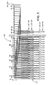
- FIG.2 schematically illustrates a delay line timing signal generator and first order voltage regulator circuit comprising one preferred embodiment of the invention.
- the delay line 5 preferably comprises series-connected CMOS inverters 10-60 not all of which are shown due to space limitations.
- the delay line 5 produces multiphasic timing signals. Representative of these signals are signals T1, T5, T8, T10, and T15, each having different phase, at the outputs of inverters 10, 14, 17, 19, and 24 respectively.
- Gates 61-102 inclusive and resistors 103-144 inclusive comprise a first order voltage regulator 6. Each gate 61-102 has a corresponding resistor 103-144 respectively connected between its output terminal and ground.
- the inputs of the gates 61-102 are preferably connected to the delay line 5 in such a way that they are distributed along its length and are activated sequentially.
- the inputs are also preferably connected to the delay line 5 in such a way that the input signals to each gate have the same relative delay between them so that all of the gates are activated and deactivated at the same supply or operating voltage level.
- one input of the AND gate 61 is connected to the input 3 of the delay line 5 at the input of the inverter 10.
- the other input of the AND gate 61 is connected to the output of the inverter 19.
- the inputs of the NOR gate 62 are connected to the out puts of the inverters 10 and 20 respectively.
- the inputs of the AND gate 63 are connected to the outputs of the inverters 11 and 21 respectively.
- the inputs of the NOR gate 64 are connected to the outputs of the inverters 12 and 22, and so on with the inputs of the last AND gate 101 being connected to the outputs of the inverters 49 and 59, and the inputs of the last NOR gate 102 being connected to the outputs of the inverters 50 and 60.
- gates connected to the outputs of odd stages of the delay line 5, i.e. gates 62, 64, 66, 68, and so on through gate 102 are NOR gates whereas gates connected to outputs of even stages of the delay line 5, i.e. gates 61, 63, 65, 67, and so on through gate 101 are AND gates.
- Typical operating parameters which will be assumed in the following description are as follows: a nominal pulse frequency of 100 kHz; and a nominal circuit operating voltage of 2.5 V.
- a typical propagation delay of a typical CMOS inverter is approximately 100 nS. Accordingly, given the nominal pulse frequency of 100 kHz, in order to ensure that only one pulse is propagating through the delay line 5 at any time, the delay line 5 must have at least 51 inverters as illustrated in the figures.
- the nominal duty cycle of each encoded digital pulse is determined by the relative delay time between input signals to each of the gates 61-102.
- a per gate propagation delay of approximately 100 nS and a ten (10) inverter delay between input signals as shown in FIG. 1 corresponds to a digital pulse having a nominal on-time of 1 ⁇ S.
- the input signal V IN is at or near its nominal level, i.e. the level at which the gates 61-102 are on the edge of being activated, increases in the on-time of the pulses reduces V REG while decreases have no effect.
- the input signal V IN exceeds its nominal value and is within the range requiring regulation, increases in the width of the pulses reduce V REG while decreases increase V REG , both approximately linearly.
- the number of gates of delay between input signals to the gates 61-102 should be correspondingly increased or decreased as appropri ate for optimum performance as described above.
- Another consideration in selecting the appropriate nominal duty cycle is that the duty cycle affects the energy per cycle delivered to the circuit. Also, a longer digital pulse on time results in more control and better control resolution over the operating voltage.
- the resistors 103-144 are selected based upon the particular application of the circuit embodying the invention. In order for the circuit to provide sufficient regulation of the operating voltage, the resistors should be selected so that when the gates 61-102 are activated, the circuit becomes the major current drawing portion of the passive circuitry with which it is associated. However, the delay line decode and voltage regulator circuit 6 obviously should not draw so much current that it lowers V IN to a level that renders the associated circuitry 4 inoperative. Within these parameters, the specific values of the resistors 103-144 are selected based on the input impedance of the associated circuitry, the number of resistors to be used, and the amount of loading required to achieve the desired regulation. For example, resistors having values ranging from 500-2000 ohms have been found suitable.
- each digital pulse transmitted by the logic control circuit 7 is input to the inverter 10 of the delay line 5.
- the pulse is inverted and delayed by each inverter as it propagates down the delay line 5.
- the output pulses of stages 10-51 are input to first terminals of corresponding gates 61-102 respectively. Even stages output positive pulses while odd stages output inverted pulses.
- the output pulses of stages 19-60 are input to second terminals of the gates 61-102 respectively.
- the logic high pulse input to the inverter 10 is also input to one terminal of the AND gate 61.
- the same uninverted signal delayed by ten inverters appears at the output of inverter 19 and is connected to the other input terminal of AND gate 61.
- inverter 10 is input to one terminal of NOR gate 62.
- inverted pulse delayed by ten inverters is output by inverter 20 to the other terminal of the NOR gate 62.
- inverter 20 is input to the inputs of the remaining gates 63-102.
- the operating voltage V REG increases and the propagation delay of the delay line inverters 10-60 decreases correspondingly.
- the propagation delay decreases until a point is reached at which the delayed pulses reach the second input terminals of the corresponding gates 61-102 before the undelayed pulses on the first input terminals have changed state. In other words, the pulses overlap at the inputs to the gates. When this occurs, the outputs of the gates 61-102 go high and current is drawn through the corresponding resistors 103-144 to ground, thus loading the power supply of the logic circuit 7.
- the voltage regulator circuit 6 draws most of the current supplied by the control logic circuit's power supply. In this way, the circuit embodying the invention inherently regulates and reduces the level of the operating voltage V REG .
- the regulator circuit 6 loads the power supply over an increasing percentage of each pulse.
- successive gates become activated simultaneously. Since the load resistances connected to the outputs of these gates are in parallel, the total resistance presented to the operating voltage is reduced and the voltage is loaded even further.
- the preferred embodiment thus provides progressive voltage regulation as a function of the level of the operating voltage.
- the pulse propagating through the delay line 5 may also be fed back from the output of an inverter, such as inverter 27 to the input 9 of the control logic circuit 7.
- the control logic circuit 7 can determine the value of the delay line delay by detecting the interval between output and input pulses on lines 8 and 9, respectively using a conventional edge-activated counter, for example. Since this interval is a function of the operating voltage V REG , the control logic circuit 7 can use the delay information to provide additional voltage regulation if needed or desired, for example, by varying the width of the encoded pulses or the amplitude of the transmitted signal or both.
- the signals on the first and second input terminals of all of the gates 61-102 have the same number of gates of delay between them, all of the gates 61-102 are activated at the same supply voltage level. However, since the inputs of the gates 61-102 are distributed along the length of the delay line 5, the gates are activated sequentially rather than simultaneously. As a result, the preferred circuit embodying the invention does not draw a large amount of current instantaneously when the gates 61-102 are activated but rather continuously loads the power supply. Such an arrangement is preferred to minimize the possibility of large, sudden rises or drops in the output of the power supply.
- FIG. 3 illustrates a delay line timing signal generator and second order voltage regulator circuit which comprises another preferred embodiment of the invention.
- the delay line 145 is comprised of series connected inverters 150-200 numbered consecutively from left to right in the figure.
- Representative timing signals T1, T5, T8, T10, and T15 are provided at the outputs of inverters 150, 154, 157, 159 and 164 respectively as in the delay line 5 of FIG. 1.
- the second order voltage regulator 146 includes a first level of gates 201-242 and associated load resistors 243-284 which are numbered consecutively from left to right in the figure. Due to space limitations, not all of the inverters, and first level gates and load resistors are illustrated.
- the gates 201-242, inverters 150-200, and load resistors 243-284 correspond identically to the gates 61-102, inverters 10-60, and load resistors 103-144 respectively of FIG. 1 and are interconnected in exactly the same manner as described above with respect to FIG. 1.
- the second order voltage regulator 146 includes a second level of gates 285-324 and corresponding load resistors 325-364, which are numbered consecutively from left to right in the figure. Not all of the second level gates and load resistors are illustrated due to space limitations.
- the resistors 325-364 are connected between the outputs of the gates 285-324 respectively and ground.
- the gates 285, 287, 289 and so on through 323 have inputs connected to outputs of even stages of the delay line 145 and are AND gates.
- the gates 286, 288 and so on through 324 have inputs connected to outputs of odd stages and are NOR gates.
- the input terminals of the gates 285-324 in the second level are connected to the inverters 150-200 so that there is a twelve-gate delay between the input signals.
- the input terminals of the first gate 285 are connected to the input of the inverter 150 and to the output of the inverter 161.
- the input terminals of the second gate 286 are connected to the outputs of the inverters 150 and 162.
- the inputs of the gate 287 are connected to the outputs of the inverters 151 and 163, and so on with the inputs of the last gate 324 being connected to the outputs of the inverters 188 and 200.
- the first level gates 201-242 are activated to load the power supply of the logic control circuit 7 at a first voltage level exceeding the nominal value of the operating voltage V REG as described above with respect to the circuit of FIG. 1.
- the second level gates 285-324 are activated at a second higher voltage level to provide additional, progressive loading of the power supply and further inhibit any increase in the operating voltage V REG .
- the voltage levels that trigger activation of the first and second level gates 201-242 and 285-324 respectively depend on the nominal operating voltage value selected, the propagation delay of the inverters, and the number of gates of delay selected between the gate input signals. The greater the selected delay, the greater the voltage level required for activation. In the embodiment of FIG.
- the second level gates 285-324 are progressively activated at an input voltage level only slightly greater than that required to activate the first level gates 201-242.
- FIG. 4 illustrates a delay line timing signal generator and third order voltage regulator circuit which comprises yet another preferred embodiment of the invention.
- the delay line 375 comprises series-connected inverters 400-450 which are numbered consecutively from left to right in the figure.
- Representative timing signals T1, T5, T8, T10, and T15 are provided at the outputs of inverters 400, 404, 407, 409, and 414.
- the third order voltage regulator 376 contains three levels of gates and associated load resistors, which are numbered consecutively in each level from left to right in the figure. Not all of the gates, resistors, and inverters are illustrated due to space limitations.
- the first level comprises gates 451-492 and associated load resistors 493-534 which are connected between the outputs of gates 451-492 respectively and ground.
- the second level comprises gates 535-574 and load resistors 575-614 which are connected between the outputs of the gates 535-574 respectively and ground.
- the third level comprises gates 620-657 and load resistors 658-695 which are connected between the outputs of the gates 620-657 respectively and ground.
- the first level gates 451-492 and load resistors 493-534 correspond identically to the first level gates 201-242 and load resistors 243-284 of the circuit of FIG. 3, and the first level gates 61-102 and load resistors 103-144 of the circuit of FIG. 1.
- the second level gates 535-574 and load resistors 575-614 correspond identically to the second level gates 285-324 and load resistors 325-364 of the circuit of FIG. 3.
- the first and second level gates 451-492 and 535-574 respectively and load resistors 493-534 and 575-614 respectively are interconnected with the delay line 375 in exactly the same manner as their counterpart devices described above with respect to FIGs. 1 and 3.
- the third level gates 620-657 are interconnected with the inverters 400-450 of the delay line 375 so that there is a fourteen-gate delay between the digital pulse signals at the first and second input terminals of each gate 620-657.
- the input terminals of the first gate 620 are connected to the input of the inverter 400 and to the output of the inverter 413.
- the input terminals of the second gate 621 are connected to the outputs of the inverters 400 and 414.
- the inputs of the third gate 622 are connected to the outputs of the inverters 401 and 415, and so on with the inputs of the last gate 576 being connected to the outputs of the inverters 436 and 450.
- the gates 620, 622, 624 and so on through gate 656 have inputs connected to outputs of even stages of the delay line 375 and are AND gates.
- the gates 621, 623 and so on through gate 657 have inputs connected to outputs of odd stages of the delay line 375 and are NOR gates.
- the first level gates 451-492 are activated to load the power supply at a first voltage level exceeding the nominal operating voltage value.
- the second level gates 535-574 are activated to further load the power supply at a second slightly greater voltage level. Because the delay between the input pulses to the third level gates 620-657 is two gates greater than the delay between the input pulses to the second level gates 535-574, the third level gates 620-657 are activated at a third voltage level which is slightly greater than the level necessary to activate the second level gates 535-574.
- the three level regulation provides even more progressive voltage regulation than the first and second level embodiments.
- the preferred second and third order regulator embodiments are made even more progressive by reducing the values of the load resistors in each level.
- the third level load resistors preferably have lower values than the second level load resistors which have lower values than the first level load resistors.
- the second and third level load resistors load the supply voltage more heavily than the first level load resistors. As a result, progressive regulation is obtained even if the second and third level gates are activated only very briefly.
- FIG. 5 A preferred variation on the basic form of the circuit embodying the invention is illustrated in FIG. 5.
- gates 752-793 and corresponding load resistors 793-834 both numbered consecutively from left to right in the figure, comprise a first order voltage regulator which is interconnected with the delay line 700 and which operates in the same manner described above with respect to FIG. 1.
- a number of the series-connected inverters making up the delay line 700 are replaced by NAND gates.
- inverters 50, 52, 54, 56, 58, and 60 are replaced with NAND gates 741, 743, 745, 747, 749, and 751 respectively.
- each NAND gate 741, 743, 745, 747, 749, and 751 is connected to the output of the preceding inverter 740, 742, 744, 746, 748, and 750 respectively.
- the other input of each NAND gate 741, 743, 745, 747, 749, and 751 is connected to the input 3 of the delay line 700.
- CMOS ring oscillator 900 comprised of multiple CMOS inverters will consume current in approximately a square law relation with variations in operating voltage, at least over the typical operating range of the CMOS devices. In other words, if the operating voltage doubles, the current consumed by the ring oscillator 900 approximately quadruples.
- a ring oscillator 900 having the same number of stages as any of the preferred circuits previously described, will not consume nearly as much current over its normal operating range as will the gates and load resistors of the previously described circuits. Accordingly, the ring oscillator embodiment may only be useful as a regulator in circuits rated for much lower current consumption. In larger circuits, for the ring oscillator to draw sufficient current to have a suitable regulation effect, it would have to have a much larger number of stages than the embodiments described above. Accordingly, the ring oscillator embodiment constitutes a less preferred alternative for such applications.
Landscapes
- Engineering & Computer Science (AREA)
- Physics & Mathematics (AREA)
- Electromagnetism (AREA)
- General Physics & Mathematics (AREA)
- Radar, Positioning & Navigation (AREA)
- Automation & Control Theory (AREA)
- Pulse Circuits (AREA)
- Electrophonic Musical Instruments (AREA)
- Control Of Eletrric Generators (AREA)
- Electrical Discharge Machining, Electrochemical Machining, And Combined Machining (AREA)
- Manipulation Of Pulses (AREA)
- Control Of Electrical Variables (AREA)
- Logic Circuits (AREA)
- Oscillators With Electromechanical Resonators (AREA)
Abstract
Description
- This invention relates generally to timing signal generator circuits and more specifically to such circuits in which the timing signals are also used to control the regulation of a supply voltage. The invention particularly relates to a circuit in which signals generated by a timing signal generator are used to automatically control the activation of loads which are used to regulate a supply voltage.
- Many digital logic circuits in use today require a source of multiphasic timing signals for their operation. It is known that ring oscillators and delay lines are inexpensive sources of such timing signals and accordingly these timing signal generators have found widespread use in both discrete and integrated logic circuits.
- It is also known that the propagation rate of such timing circuits, when constructed of CMOS devices such as CMOS inventers, varies predictably with variations in the supply voltage. Accordingly, it has been recognized that the interval between timing pulses or the frequency of such pulses provides an indication of the supply voltage level and can be used by conventional voltage regulators as a control parameter to regulate the supply voltage. See, for example, Hashimoto U.S. Patent No. 4,358,728.
- However, conventional voltage regulation circuitry adds expense and complexity to circuits. In addition, in the case of integrated circuits, it takes up precious substrate space that could otherwise be used to fabricate additional logic components.
- Moreover, many miniature passive circuits in use today derive operating power from power/timing signals transmitted by remotely located control circuits. Such circuits are often found, for example, in miniature transponder systems, implantable medical devices, and portable data retrieval applications. See U.S. Patent Nos. 3,859,624 to Kriofsky et al.; 4,408,608 to Daly et al.; 4,533,988 to Daly et al.; and 4,196,418 to Kip et al. Circuits of this type typically are designed to operate on low power and to take up minimum space. Accordingly, it is particularly desirable in these types of circuits to regulate the operating voltage derived from the power/timing signals without the requirement of additional voltage regulation circuitry.
- Accordingly, it is an object of the invention to provide a timing signal generator circuit that generates multiphasic timing signals while regulating the operating or supply voltage of the circuit.
- It is another object to provide such a circuit that regulates the operating voltage without the need for conventional voltage regulation circuitry, or that can also be utilized in conjunction with such circuitry to achieve additional voltage regulation.
- It is still another object to provide such a circuit that is simple but flexible in design, construction, and operation, and that can be conveniently and inexpensively fabricated in integrated circuit form.
- The foregoing objects and attendant advantages are achieved by providing a digital timing signal generator and voltage regulator circuit in which in broad form a timing signal generator generates timing signals having timing relationship related to the level of the operating voltage, and a regulator circuit connected to the timing signal generator responds to the timing relationship of the timing signals to load the operating voltage in order to regulate it.
- In one aspect, the timing generator propagates a signal at a rate related to the level of its supply voltage to generate at least one timing signal. When the timing relationship is less than a predetermined minimum value, gates are activated to selectively load the supply voltage in order to regulate it.
- In another aspect, a delay line propagates signals to generate at least one timing signal. A plurality of gates having inputs connected to selected stages of the delay line receive selected timing signals. When the signals overlap, the gates are activated and load means connected thereto load the supply voltage to regulate it.
- In still another aspect, a circuit continuously propagates a signal to generate at least one timing signal. The circuit is arranged and constructed to consume current in approximately a square relationship with increases in its supply voltage in order to regulate the voltage.
- The novel features that are believed to be characteristic of the invention are set forth in the appended claims. The invention itself will be best understood by reference to the following detailed description of several circuits which constitute preferred embodiments of the invention, in conjunction with the drawing, in which;
- FIG. 1 is a block diagram illustrating the preferred mode of using the delay line timing signal generator and voltage regulator circuit embodying the invention;
- FIG. 2 is a schematic diagram illustrating the details of a delay line timing signal generator and first order voltage regulator circuit comprising one preferred embodiment of the invention;
- FIG. 3 is a schematic diagram illustrating the details of a delay line timing signal generator and second order voltage regulator circuit comprising another preferred embodiment of the invention;
- FIG. 4 is a schematic diagram illustrating the details of a delay line timing signal generator and third order voltage regulator circuit comprising yet another preferred embodiment of the invention;
- FIG. 5 is a schematic diagram illustrating the details of a delay line timing signal generator and first order voltage regulator circuit according to the invention which has been modified to extinguish signals propagating in the "tail" of the delay line when a pulse is received at the "head" of the delay line, and
- FIG. 6 is a schematic diagram of a ring oscillator comprising an alternative embodiment of the invention.
- With reference to the drawing, FIG. 1 generally illustrates the preferred form of the invention which broadly comprises a timing signal generator such as a
delay line 5 and an associated delay line decode and voltage regulator 6 which receives and is reponsive to the generated timing signals. In the presently preferred form of the invention, thedelay line 5 and voltage regulator 6 are fabricated along with a signal detect and power circuit 2 and various logic circuits 4 in an integrated circuit chip (IC). The IC is suitably fabricated using conventional CMOS fabrication processes known to those skilled in the art. - In one preferred form, the IC receives its operating power from an external
control logic circuit 7 which is powered by its own power supply. In this form, thecontrol logic circuit 7 includes conventional circuitry for generating and transmitting a power/timing signal VIN, on an output 8. The power/timing signal VIN comprises a carrier signal modulated with digital pulses having predetermined nominal frequency, amplitude, and duty cycle. Such control logic circuitry is conventional and does not comprise part of the present invention. See, for example, the circuits described in the various United States Patents cited above. - The power/timing signal VIN is input to the IC on a
signal input terminal 8a. The output 8 of thecontrol logic circuit 7 and thesignal input terminal 8a of the IC are preferably isolated by inductive coupling, although capacitive, resistive, or optical coupling may also be employed. However, whatever coupling arrangement is used should preferably have a relatively high resistance component compared to the input resistance of the IC. Thus, in the case of inductive coupling, for example, a low efficiency coupling is preferred. - The
signal input 8a is connected to an input of the signal detect and power circuit 2. The signal detect and power circuit 2 detects the digital pulses on the modulated carrier and serially outputs corresponding digital pulses online 3. At the same time, it also derives from the modulated carrier a supply or operating voltage VREG which is conducted to the supply inputs of thedelay line 5, the voltage regulator 6, and the various logic circuits 4 on line 1. The signal detect and power circuit 2 is a conventional circuit and is familiar to those skilled in the art. One form of the circuit that is particularly preferred for use with the present invention is described and illustrated in the applicant's co-pending U.S. Application Serial No. 818,469 filed January 13, 1986. - The
delay line 5 receives the digital pulses online 3 and generates multiphasic timing signals therefrom. The timing signals are received and used by the various logic circuits 4 to carry out their respective logic functions. The timing signals are also received by the voltage regulator 6 which decodes them and, if necessary, loads the operating voltage VREG with a predetermined load in order to regulate and reduce it to a predetermined nominal value. The delay line may also output one of the digital timing signals on anoutput terminal 9a to an input 9 of thecontrol logic 7. Theoutput 9a and input 9 are preferably isolated as described above. Preferably, the digital timing signal onlines 9 and 9a can share the isolation means with the power/timing signal onlines 8 and 8a. Thecontrol logic 7 may determine the delay between output pulses on line 8 and timing pulses on the input 9 as an indication of the operating voltage VREG and use this data to provide additional regulation by altering the width of the encoded digital pulses or the amplitude of the power/timing signal VIN on output 8. Thecontrol logic 7 may also use the signals on line 9 to regulate the frequency of the encoded digital pulses on output 8. - FIG.2 schematically illustrates a delay line timing signal generator and first order voltage regulator circuit comprising one preferred embodiment of the invention. The
delay line 5 preferably comprises series-connected CMOS inverters 10-60 not all of which are shown due to space limitations. Thedelay line 5 produces multiphasic timing signals. Representative of these signals are signals T1, T5, T8, T10, and T15, each having different phase, at the outputs ofinverters - Gates 61-102 inclusive and resistors 103-144 inclusive comprise a first order voltage regulator 6. Each gate 61-102 has a corresponding resistor 103-144 respectively connected between its output terminal and ground. The inputs of the gates 61-102 are preferably connected to the
delay line 5 in such a way that they are distributed along its length and are activated sequentially. The inputs are also preferably connected to thedelay line 5 in such a way that the input signals to each gate have the same relative delay between them so that all of the gates are activated and deactivated at the same supply or operating voltage level. - Accordingly, one input of the AND
gate 61 is connected to theinput 3 of thedelay line 5 at the input of the inverter 10. The other input of the ANDgate 61 is connected to the output of theinverter 19. The inputs of the NORgate 62 are connected to the out puts of theinverters 10 and 20 respectively. The inputs of the ANDgate 63 are connected to the outputs of theinverters 11 and 21 respectively. The inputs of the NORgate 64 are connected to the outputs of theinverters 12 and 22, and so on with the inputs of the last ANDgate 101 being connected to the outputs of theinverters 49 and 59, and the inputs of the last NORgate 102 being connected to the outputs of theinverters - From the foregoing it is apparent that there is a relative delay of ten (10) inverters between the input signals to each gate. It is also apparent that the inputs of the gates 61-102 are distributed along the length of the
delay line 5 so that each input signal to each gate except gate 10 is delayed by one inverter with respect to the corresponding input signal to the preceding gate. In the presently preferred embodiment, gates connected to the outputs of odd stages of thedelay line 5, i.e.gates gate 102 are NOR gates whereas gates connected to outputs of even stages of thedelay line 5, i.e.gates gate 101 are AND gates. - It is preferable that only one digital pulse propagate through the
delay line 5 at any given time. On the other hand, it is also preferable that there be a minimum of delay between successive pulses propagating through thedelay line 5 so that the amount of time the operating voltage is unregulated is minimized. These operating characteristics are obtained by selecting adelay line 5 having an appropriate length, i.e. having an appropriate number of stages, based on the desired nominal operating voltage, the desired nominal frequency, and the per gate propagation delay of the particular devices selected for use, which as those skilled in the art are aware is readily available from the various manufacturer's data sheets. Typical operating parameters which will be assumed in the following description are as follows: a nominal pulse frequency of 100 kHz; and a nominal circuit operating voltage of 2.5 V. At the selected nominal operating voltage, a typical propagation delay of a typical CMOS inverter is approximately 100 nS. Accordingly, given the nominal pulse frequency of 100 kHz, in order to ensure that only one pulse is propagating through thedelay line 5 at any time, thedelay line 5 must have at least 51 inverters as illustrated in the figures. - The nominal duty cycle of each encoded digital pulse is determined by the relative delay time between input signals to each of the gates 61-102. Thus, with respect to the nominal values above, a per gate propagation delay of approximately 100 nS and a ten (10) inverter delay between input signals as shown in FIG. 1 corresponds to a digital pulse having a nominal on-time of 1µS. When the amplitude of the input signal VIN is below its nominal value, moderate changes in the width of the pulses have no effect on VREG. When the input signal VIN is at or near its nominal level, i.e. the level at which the gates 61-102 are on the edge of being activated, increases in the on-time of the pulses reduces VREG while decreases have no effect. When the input signal VIN exceeds its nominal value and is within the range requiring regulation, increases in the width of the pulses reduce VREG while decreases increase VREG, both approximately linearly.
- If it is desired to extend or shorten the nominal on-time of the pulses, the number of gates of delay between input signals to the gates 61-102 should be correspondingly increased or decreased as appropri ate for optimum performance as described above. Another consideration in selecting the appropriate nominal duty cycle is that the duty cycle affects the energy per cycle delivered to the circuit. Also, a longer digital pulse on time results in more control and better control resolution over the operating voltage.
- The resistors 103-144 are selected based upon the particular application of the circuit embodying the invention. In order for the circuit to provide sufficient regulation of the operating voltage, the resistors should be selected so that when the gates 61-102 are activated, the circuit becomes the major current drawing portion of the passive circuitry with which it is associated. However, the delay line decode and voltage regulator circuit 6 obviously should not draw so much current that it lowers VIN to a level that renders the associated circuitry 4 inoperative. Within these parameters, the specific values of the resistors 103-144 are selected based on the input impedance of the associated circuitry, the number of resistors to be used, and the amount of loading required to achieve the desired regulation. For example, resistors having values ranging from 500-2000 ohms have been found suitable.
- In operation, each digital pulse transmitted by the
logic control circuit 7 is input to the inverter 10 of thedelay line 5. The pulse is inverted and delayed by each inverter as it propagates down thedelay line 5. The output pulses of stages 10-51 are input to first terminals of corresponding gates 61-102 respectively. Even stages output positive pulses while odd stages output inverted pulses. The output pulses of stages 19-60 are input to second terminals of the gates 61-102 respectively. Accordingly, the logic high pulse input to the inverter 10 is also input to one terminal of the ANDgate 61. The same uninverted signal delayed by ten inverters appears at the output ofinverter 19 and is connected to the other input terminal of ANDgate 61. Likewise, the inverted pulse at the output of inverter 10 is input to one terminal of NORgate 62. The same inverted pulse delayed by ten inverters is output byinverter 20 to the other terminal of the NORgate 62. The same applies to the inputs of the remaining gates 63-102. - As long as the
control logic circuit 7 continues to transmit VIN with the encoded digital pulses at the nominal frequency and duty cycle, and with the appropriate amplitude to keep the operating voltage VREG of thedelay line 5 at the nominal value, there is no overlap between the delayed and undelayed pulses at the input terminals of the gates 61-102. In other words, with respect to the even stages, by the time the delayed logic high pulse reaches the second input terminal of the corresponding AND gate, the undelayed pulse on the first input terminal has changed state and the AND gate is not activated. The same result occurs with respect to the inverted pulses generated by the odd stages and the corresponding NOR gates. As a result, no current is drawn through the resistors 103-144 to ground. - As the amplitude of the power/timing signal VIN transmitted by the
control logic circuit 7 increases, the operating voltage VREG increases and the propagation delay of the delay line inverters 10-60 decreases correspondingly. As the operating voltage VREG increases, the propagation delay decreases until a point is reached at which the delayed pulses reach the second input terminals of the corresponding gates 61-102 before the undelayed pulses on the first input terminals have changed state. In other words, the pulses overlap at the inputs to the gates. When this occurs, the outputs of the gates 61-102 go high and current is drawn through the corresponding resistors 103-144 to ground, thus loading the power supply of thelogic circuit 7. Preferably, when the gates 61-102 are activated, the voltage regulator circuit 6 draws most of the current supplied by the control logic circuit's power supply. In this way, the circuit embodying the invention inherently regulates and reduces the level of the operating voltage VREG. - As the amplitude of the transmitted power/timing signal VIN continues to increase, the amount of overlap between the undelayed and delayed pulses increases correspondingly. As a result, the regulator circuit 6 loads the power supply over an increasing percentage of each pulse. In addition, as the delayed and undelayed input pulses increasingly overlap, successive gates become activated simultaneously. Since the load resistances connected to the outputs of these gates are in parallel, the total resistance presented to the operating voltage is reduced and the voltage is loaded even further. The preferred embodiment thus provides progressive voltage regulation as a function of the level of the operating voltage.
- When the amplitude of VIN stops increasing, the degree of overlap and the percentage of each pulse that is loaded also stops increasing. During this equilibrium condition, the voltage VREG will be slightly above its nominal value. As the amplitude of VIN decreases, the degree of overlap and the percentage of each pulse that is loaded decreases accordingly until at some point at or near the nominal value of VREG there is no longer any overlap between the undelayed and delayed pulses.
- As previously touched upon, the pulse propagating through the
delay line 5 may also be fed back from the output of an inverter, such asinverter 27 to the input 9 of thecontrol logic circuit 7. Thecontrol logic circuit 7 can determine the value of the delay line delay by detecting the interval between output and input pulses on lines 8 and 9, respectively using a conventional edge-activated counter, for example. Since this interval is a function of the operating voltage VREG, thecontrol logic circuit 7 can use the delay information to provide additional voltage regulation if needed or desired, for example, by varying the width of the encoded pulses or the amplitude of the transmitted signal or both. - Since the signals on the first and second input terminals of all of the gates 61-102 have the same number of gates of delay between them, all of the gates 61-102 are activated at the same supply voltage level. However, since the inputs of the gates 61-102 are distributed along the length of the
delay line 5, the gates are activated sequentially rather than simultaneously. As a result, the preferred circuit embodying the invention does not draw a large amount of current instantaneously when the gates 61-102 are activated but rather continuously loads the power supply. Such an arrangement is preferred to minimize the possibility of large, sudden rises or drops in the output of the power supply. - FIG. 3 illustrates a delay line timing signal generator and second order voltage regulator circuit which comprises another preferred embodiment of the invention. The
delay line 145 is comprised of series connected inverters 150-200 numbered consecutively from left to right in the figure. Representative timing signals T1, T5, T8, T10, and T15 are provided at the outputs ofinverters delay line 5 of FIG. 1. The secondorder voltage regulator 146 includes a first level of gates 201-242 and associated load resistors 243-284 which are numbered consecutively from left to right in the figure. Due to space limitations, not all of the inverters, and first level gates and load resistors are illustrated. The gates 201-242, inverters 150-200, and load resistors 243-284 correspond identically to the gates 61-102, inverters 10-60, and load resistors 103-144 respectively of FIG. 1 and are interconnected in exactly the same manner as described above with respect to FIG. 1. - In addition, the second
order voltage regulator 146 includes a second level of gates 285-324 and corresponding load resistors 325-364, which are numbered consecutively from left to right in the figure. Not all of the second level gates and load resistors are illustrated due to space limitations. The resistors 325-364 are connected between the outputs of the gates 285-324 respectively and ground. Similarly to the first order regulator of FIG. 2, the gates 285, 287, 289 and so on through 323 have inputs connected to outputs of even stages of thedelay line 145 and are AND gates. The gates 286, 288 and so on through 324 have inputs connected to outputs of odd stages and are NOR gates. - In contrast to the ten-gate delay between the input signals to each of the gates 201-242 in the first level, the input terminals of the gates 285-324 in the second level are connected to the inverters 150-200 so that there is a twelve-gate delay between the input signals. Thus, for example, the input terminals of the first gate 285 are connected to the input of the
inverter 150 and to the output of the inverter 161. The input terminals of the second gate 286 are connected to the outputs of theinverters 150 and 162. The inputs of the gate 287 are connected to the outputs of the inverters 151 and 163, and so on with the inputs of the last gate 324 being connected to the outputs of theinverters - In the circuit of FIG. 3, the first level gates 201-242 are activated to load the power supply of the
logic control circuit 7 at a first voltage level exceeding the nominal value of the operating voltage VREG as described above with respect to the circuit of FIG. 1. The second level gates 285-324 are activated at a second higher voltage level to provide additional, progressive loading of the power supply and further inhibit any increase in the operating voltage VREG. The voltage levels that trigger activation of the first and second level gates 201-242 and 285-324 respectively depend on the nominal operating voltage value selected, the propagation delay of the inverters, and the number of gates of delay selected between the gate input signals. The greater the selected delay, the greater the voltage level required for activation. In the embodiment of FIG. 3, for example, there is only a two-gate delay difference between the gate input signals at the first and second levels. Accordingly, the second level gates 285-324 are progressively activated at an input voltage level only slightly greater than that required to activate the first level gates 201-242. - FIG. 4 illustrates a delay line timing signal generator and third order voltage regulator circuit which comprises yet another preferred embodiment of the invention. The
delay line 375 comprises series-connected inverters 400-450 which are numbered consecutively from left to right in the figure. Representative timing signals T1, T5, T8, T10, and T15 are provided at the outputs ofinverters order voltage regulator 376 contains three levels of gates and associated load resistors, which are numbered consecutively in each level from left to right in the figure. Not all of the gates, resistors, and inverters are illustrated due to space limitations. - The first level comprises gates 451-492 and associated load resistors 493-534 which are connected between the outputs of gates 451-492 respectively and ground. The second level comprises gates 535-574 and load resistors 575-614 which are connected between the outputs of the gates 535-574 respectively and ground. The third level comprises gates 620-657 and load resistors 658-695 which are connected between the outputs of the gates 620-657 respectively and ground.
- The first level gates 451-492 and load resistors 493-534 correspond identically to the first level gates 201-242 and load resistors 243-284 of the circuit of FIG. 3, and the first level gates 61-102 and load resistors 103-144 of the circuit of FIG. 1. The second level gates 535-574 and load resistors 575-614 correspond identically to the second level gates 285-324 and load resistors 325-364 of the circuit of FIG. 3. The first and second level gates 451-492 and 535-574 respectively and load resistors 493-534 and 575-614 respectively are interconnected with the
delay line 375 in exactly the same manner as their counterpart devices described above with respect to FIGs. 1 and 3. - The third level gates 620-657 are interconnected with the inverters 400-450 of the
delay line 375 so that there is a fourteen-gate delay between the digital pulse signals at the first and second input terminals of each gate 620-657. Thus, for example, the input terminals of the first gate 620 are connected to the input of theinverter 400 and to the output of the inverter 413. The input terminals of the second gate 621 are connected to the outputs of theinverters inverters inverters delay line 375 and are AND gates. The gates 621, 623 and so on through gate 657 have inputs connected to outputs of odd stages of thedelay line 375 and are NOR gates. - In the circuit of FIG. 4, the first level gates 451-492 are activated to load the power supply at a first voltage level exceeding the nominal operating voltage value. The second level gates 535-574 are activated to further load the power supply at a second slightly greater voltage level. Because the delay between the input pulses to the third level gates 620-657 is two gates greater than the delay between the input pulses to the second level gates 535-574, the third level gates 620-657 are activated at a third voltage level which is slightly greater than the level necessary to activate the second level gates 535-574. Thus, the three level regulation provides even more progressive voltage regulation than the first and second level embodiments.
- The preferred second and third order regulator embodiments are made even more progressive by reducing the values of the load resistors in each level. Thus, the third level load resistors preferably have lower values than the second level load resistors which have lower values than the first level load resistors. With this arrangement, the second and third level load resistors load the supply voltage more heavily than the first level load resistors. As a result, progressive regulation is obtained even if the second and third level gates are activated only very briefly.
- A preferred variation on the basic form of the circuit embodying the invention is illustrated in FIG. 5. As shown, gates 752-793 and corresponding load resistors 793-834 both numbered consecutively from left to right in the figure, comprise a first order voltage regulator which is interconnected with the
delay line 700 and which operates in the same manner described above with respect to FIG. 1. However, in the preferred variation a number of the series-connected inverters making up thedelay line 700 are replaced by NAND gates. Specifically, referring to FIG. 1,inverters NAND gates delay line 700 are alternately NAND gates and inverters. One input of eachNAND gate inverter NAND gate input 3 of thedelay line 700. - In this embodiment, if a power pulse should be input to the head of the
delay line 700 before the preceding power pulse has completely propagated through the tail of thedelay line 700, the preceding power pulse will be extinguished by maintaining the NAND gate outputs low so that it cannot activate any of the last eleven gates 782-793. This modification compensates for variations in the frequency of the power pulses transmitted by thecontrol logic circuit 7 and allows the circuit embodying the invention to be used over a wider range of operating conditions. - Another variation of the invention is to util ize a CMOS ring oscillator as illustrated in FIG. 6 in place of the previously described timing signal generator and voltage regulator circuits described above. It has been found that a
ring oscillator 900 comprised of multiple CMOS inverters will consume current in approximately a square law relation with variations in operating voltage, at least over the typical operating range of the CMOS devices. In other words, if the operating voltage doubles, the current consumed by thering oscillator 900 approximately quadruples. - However, it is to be understood that a
ring oscillator 900 having the same number of stages as any of the preferred circuits previously described, will not consume nearly as much current over its normal operating range as will the gates and load resistors of the previously described circuits. Accordingly, the ring oscillator embodiment may only be useful as a regulator in circuits rated for much lower current consumption. In larger circuits, for the ring oscillator to draw sufficient current to have a suitable regulation effect, it would have to have a much larger number of stages than the embodiments described above. Accordingly, the ring oscillator embodiment constitutes a less preferred alternative for such applications. - What have been described are certain aspects of various digital timing signal generator and voltage regulator circuits which constitute presently preferred embodiments of the invention. It is understood that the foregoing description and accompanying illustration are merely exemplary and are in no way intended to limit the scope of the invention, which is defined by the appended claims. Various changes and modifications to the preferred embodiments will be apparent to those skilled in the art. Such changes and modifications may include but are not limited to changes in the length or number of stages of the delay lines, changes in the number and types of gates comprising the delay lines and voltage regulators, changes in the nominal values of various parameters and circuit elements, changes in the interconnections of the basic elements, and the like. Such changes and modifications can be made without departing from the spirit and scope of the invention. Accordingly, it is intended that all such changes and modifications and all other equivalents be covered by the appended claims.
Claims (19)
means for generating timing signals having a timing relationship related to the level of an operating voltage associated with said means for generating; and
means connected to said generating means and responsive to said timing relationship for loading said operating voltage to regulate it.
means for propagating a signal to generate timing signals, said means having a rate of propagation related to the level of said operating voltage.
gate means connected to said generating means for receiving said timing signals, said gate means being activated when the timing relationship between said signals is less than a predetermined minimum value; and
load means connected to said gate means for loading said operating voltage when said gate means are activated.
gate means connected to said means for propagating for receiving said timing signals and the same said timing signals offset by a timing interval determined by said propagation rate of said means for propagating;
said gate means being activated when the timing interval between said signals and said offset signals is less than a predetermined value; and
load means connected to said gate means for loading said operating voltage when said gate means are activated.
a delay line having a plurality of stages for generating timing signals with timing relationship related to the level of a supply voltage;
a plurality of gates having inputs connected to selected stages of said delay line for receiving selected timing signals, said gates being activated when said selected signals overlap; and
a corresponding plurality of load resistors connected to the outputs of said plurality of gates for loading said supply voltage when said gates are activated in order to regulate said supply voltage.
a delay line having a plurality of stages for receiving and propagating said encoded digital signals to generate timing signals for use by said circuit, said timing signals having timing relationship related to the level of said operating voltage;
a plurality of gates having inputs connected to selected stages of said delay line for receiving selected timing signals, said gates being activated when said selected timing signals overlap; and
a corresponding plurality of load means connected to the outputs of said gates for loading said power supply when said gates are activated in order to regulate said operating voltage.
means powered by an operating voltage for continuously propagating a signal to generate at least one timing signal, said means consuming increased current in response to increases in said operating voltage in order to regulate said operating voltage.
said ring oscillator having a plurality of CMOS gates for consuming current generated by said power supply in approximately a square relationship with increases in said operating voltage in order to regulate said operating voltage.
Priority Applications (1)
| Application Number | Priority Date | Filing Date | Title |
|---|---|---|---|
| AT87114416T ATE92203T1 (en) | 1986-10-23 | 1987-10-02 | DIGITAL PULSE SIGNAL GENERATOR AND VOLTAGE REGULATOR CIRCUIT. |
Applications Claiming Priority (2)
| Application Number | Priority Date | Filing Date | Title |
|---|---|---|---|
| US92238986A | 1986-10-23 | 1986-10-23 | |
| US922389 | 1986-10-23 |
Publications (3)
| Publication Number | Publication Date |
|---|---|
| EP0264691A2 true EP0264691A2 (en) | 1988-04-27 |
| EP0264691A3 EP0264691A3 (en) | 1989-05-24 |
| EP0264691B1 EP0264691B1 (en) | 1993-07-28 |
Family
ID=25446966
Family Applications (1)
| Application Number | Title | Priority Date | Filing Date |
|---|---|---|---|
| EP87114416A Expired - Lifetime EP0264691B1 (en) | 1986-10-23 | 1987-10-02 | Digital timing signal generator and voltage regulator circuit |
Country Status (7)
| Country | Link |
|---|---|
| EP (1) | EP0264691B1 (en) |
| JP (1) | JPS63121315A (en) |
| AT (1) | ATE92203T1 (en) |
| AU (1) | AU599711B2 (en) |
| CA (1) | CA1284826C (en) |
| DE (1) | DE3786741T2 (en) |
| ES (1) | ES2043628T3 (en) |
Cited By (2)
| Publication number | Priority date | Publication date | Assignee | Title |
|---|---|---|---|---|
| DE10024783A1 (en) * | 2000-05-19 | 2001-11-22 | Micronas Munich Gmbh | Digital clock generator outputs most significant data bit of fed back digital sum as clock signal and digital phase error derived from least significant bit and incremental value |
| US7271558B2 (en) | 2003-07-22 | 2007-09-18 | Siemens Aktiengesellschaft | Method for the generation of electrical pulses |
Families Citing this family (1)
| Publication number | Priority date | Publication date | Assignee | Title |
|---|---|---|---|---|
| US20220407506A1 (en) * | 2021-06-10 | 2022-12-22 | Microsoft Technology Licensing, Llc | Clock monitor |
Citations (4)
| Publication number | Priority date | Publication date | Assignee | Title |
|---|---|---|---|---|
| US3445752A (en) * | 1965-07-19 | 1969-05-20 | Patelhold Patentvertungs Und E | Direct current regulated power supply |
| EP0012839A1 (en) * | 1978-12-22 | 1980-07-09 | International Business Machines Corporation | Method and device for adjusting the different time delays of semiconductor chips by changing the working voltage |
| GB2050097A (en) * | 1979-04-10 | 1980-12-31 | Citizen Watch Co Ltd | Voltage control circuit |
| US4445083A (en) * | 1981-08-26 | 1984-04-24 | Honeywell Information Systems Inc. | Integrated circuit compensatory regulator apparatus |
-
1987
- 1987-10-02 AT AT87114416T patent/ATE92203T1/en not_active IP Right Cessation
- 1987-10-02 EP EP87114416A patent/EP0264691B1/en not_active Expired - Lifetime
- 1987-10-02 DE DE87114416T patent/DE3786741T2/en not_active Expired - Fee Related
- 1987-10-02 ES ES87114416T patent/ES2043628T3/en not_active Expired - Lifetime
- 1987-10-19 AU AU79887/87A patent/AU599711B2/en not_active Ceased
- 1987-10-21 CA CA000549888A patent/CA1284826C/en not_active Expired - Fee Related
- 1987-10-23 JP JP62269157A patent/JPS63121315A/en active Pending
Patent Citations (4)
| Publication number | Priority date | Publication date | Assignee | Title |
|---|---|---|---|---|
| US3445752A (en) * | 1965-07-19 | 1969-05-20 | Patelhold Patentvertungs Und E | Direct current regulated power supply |
| EP0012839A1 (en) * | 1978-12-22 | 1980-07-09 | International Business Machines Corporation | Method and device for adjusting the different time delays of semiconductor chips by changing the working voltage |
| GB2050097A (en) * | 1979-04-10 | 1980-12-31 | Citizen Watch Co Ltd | Voltage control circuit |
| US4445083A (en) * | 1981-08-26 | 1984-04-24 | Honeywell Information Systems Inc. | Integrated circuit compensatory regulator apparatus |
Cited By (4)
| Publication number | Priority date | Publication date | Assignee | Title |
|---|---|---|---|---|
| DE10024783A1 (en) * | 2000-05-19 | 2001-11-22 | Micronas Munich Gmbh | Digital clock generator outputs most significant data bit of fed back digital sum as clock signal and digital phase error derived from least significant bit and incremental value |
| DE10024783C2 (en) * | 2000-05-19 | 2002-05-08 | Micronas Munich Gmbh | Digital clock generator |
| US7339412B2 (en) | 2000-05-19 | 2008-03-04 | Micronas Gmbh | Digital clock generator |
| US7271558B2 (en) | 2003-07-22 | 2007-09-18 | Siemens Aktiengesellschaft | Method for the generation of electrical pulses |
Also Published As
| Publication number | Publication date |
|---|---|
| EP0264691B1 (en) | 1993-07-28 |
| AU7988787A (en) | 1988-04-28 |
| ATE92203T1 (en) | 1993-08-15 |
| DE3786741T2 (en) | 1993-11-11 |
| AU599711B2 (en) | 1990-07-26 |
| CA1284826C (en) | 1991-06-11 |
| EP0264691A3 (en) | 1989-05-24 |
| DE3786741D1 (en) | 1993-09-02 |
| JPS63121315A (en) | 1988-05-25 |
| ES2043628T3 (en) | 1994-01-01 |
Similar Documents
| Publication | Publication Date | Title |
|---|---|---|
| EP0737906B1 (en) | A power system and method of providing a supply voltage to a computer | |
| JP3547854B2 (en) | Buffer circuit with drive current adjustment function | |
| CN100511098C (en) | Adaptive voltage scaling clock generator for use in a large scale digital processing component and method of operating the same | |
| US5894423A (en) | Data processing system having an auto-ranging low voltage detection circuit | |
| US5719534A (en) | Semiconductor integrated circuit having low power consumption oscillator | |
| US7298200B2 (en) | Voltage generation circuits for supplying an internal voltage to an internal circuit and related methods | |
| US5227672A (en) | Digital clock selection and changeover apparatus | |
| US5077488A (en) | Digital timing signal generator and voltage regulation circuit | |
| JPH11127547A (en) | On/off controller for power unit | |
| US6014051A (en) | Current compensated clock for a microcircuit | |
| EP0264691A2 (en) | Digital timing signal generator and voltage regulator circuit | |
| US6847198B2 (en) | Frequency sensing voltage regulator | |
| US5754037A (en) | Digitally adaptive biasing regulator | |
| US4535305A (en) | Transmission gate relaxation oscillator having comparator | |
| EP1180689A2 (en) | Frequency determination circuit for a data processing unit | |
| KR100232783B1 (en) | Voltage-controlled apparatus for battery-powered electronic devices | |
| EP1483788B1 (en) | A dynamic voltage scaling scheme for an on-die voltage differentiator design | |
| US4916332A (en) | Timing and supply bias circuit using one capacitor | |
| US5391927A (en) | Apparatus for improving rise characteristics of direct current power supply | |
| EP3282583A1 (en) | Oscillator circuit | |
| CN113111030B (en) | System on chip and control method thereof | |
| US11223221B2 (en) | Power management | |
| JP3460802B2 (en) | Semiconductor device | |
| JP2003332891A (en) | Oscillator circuit, semi-conductor device including the same, semi-conductor storage device, and method for controlling the oscillator circuit | |
| EP1654629B1 (en) | Modifying clock signals output by an integrated circuit |
Legal Events
| Date | Code | Title | Description |
|---|---|---|---|
| PUAI | Public reference made under article 153(3) epc to a published international application that has entered the european phase |
Free format text: ORIGINAL CODE: 0009012 |
|
| AK | Designated contracting states |
Kind code of ref document: A2 Designated state(s): AT BE CH DE ES FR GB IT LI NL |
|
| PUAL | Search report despatched |
Free format text: ORIGINAL CODE: 0009013 |
|
| AK | Designated contracting states |
Kind code of ref document: A3 Designated state(s): AT BE CH DE ES FR GB IT LI NL |
|
| 17P | Request for examination filed |
Effective date: 19890722 |
|
| 17Q | First examination report despatched |
Effective date: 19910213 |
|
| GRAA | (expected) grant |
Free format text: ORIGINAL CODE: 0009210 |
|
| AK | Designated contracting states |
Kind code of ref document: B1 Designated state(s): AT BE CH DE ES FR GB IT LI NL |
|
| REF | Corresponds to: |
Ref document number: 92203 Country of ref document: AT Date of ref document: 19930815 Kind code of ref document: T |
|
| REF | Corresponds to: |
Ref document number: 3786741 Country of ref document: DE Date of ref document: 19930902 |
|
| PGFP | Annual fee paid to national office [announced via postgrant information from national office to epo] |
Ref country code: GB Payment date: 19930917 Year of fee payment: 7 Ref country code: AT Payment date: 19930917 Year of fee payment: 7 |
|
| ET | Fr: translation filed | ||
| ITF | It: translation for a ep patent filed | ||
| PGFP | Annual fee paid to national office [announced via postgrant information from national office to epo] |
Ref country code: BE Payment date: 19931012 Year of fee payment: 7 |
|
| PGFP | Annual fee paid to national office [announced via postgrant information from national office to epo] |
Ref country code: FR Payment date: 19931013 Year of fee payment: 7 |
|
| PGFP | Annual fee paid to national office [announced via postgrant information from national office to epo] |
Ref country code: ES Payment date: 19931014 Year of fee payment: 7 |
|
| PGFP | Annual fee paid to national office [announced via postgrant information from national office to epo] |
Ref country code: DE Payment date: 19931026 Year of fee payment: 7 |
|
| PGFP | Annual fee paid to national office [announced via postgrant information from national office to epo] |
Ref country code: NL Payment date: 19931031 Year of fee payment: 7 |
|
| REG | Reference to a national code |
Ref country code: ES Ref legal event code: FG2A Ref document number: 2043628 Country of ref document: ES Kind code of ref document: T3 |
|
| PGFP | Annual fee paid to national office [announced via postgrant information from national office to epo] |
Ref country code: CH Payment date: 19940104 Year of fee payment: 7 |
|
| PLBE | No opposition filed within time limit |
Free format text: ORIGINAL CODE: 0009261 |
|
| STAA | Information on the status of an ep patent application or granted ep patent |
Free format text: STATUS: NO OPPOSITION FILED WITHIN TIME LIMIT |
|
| 26N | No opposition filed | ||
| PG25 | Lapsed in a contracting state [announced via postgrant information from national office to epo] |
Ref country code: AT Effective date: 19941002 Ref country code: GB Effective date: 19941002 |
|
| PG25 | Lapsed in a contracting state [announced via postgrant information from national office to epo] |
Ref country code: ES Free format text: LAPSE BECAUSE OF THE APPLICANT RENOUNCES Effective date: 19941003 |
|
| PG25 | Lapsed in a contracting state [announced via postgrant information from national office to epo] |
Ref country code: CH Effective date: 19941031 Ref country code: BE Effective date: 19941031 Ref country code: LI Effective date: 19941031 |
|
| BERE | Be: lapsed |
Owner name: ABBOTT LABORATORIES Effective date: 19941031 |
|
| PG25 | Lapsed in a contracting state [announced via postgrant information from national office to epo] |
Ref country code: NL Effective date: 19950501 |
|
| GBPC | Gb: european patent ceased through non-payment of renewal fee |
Effective date: 19941002 |
|
| NLV4 | Nl: lapsed or anulled due to non-payment of the annual fee | ||
| PG25 | Lapsed in a contracting state [announced via postgrant information from national office to epo] |
Ref country code: FR Effective date: 19950630 |
|
| REG | Reference to a national code |
Ref country code: CH Ref legal event code: PL |
|
| PG25 | Lapsed in a contracting state [announced via postgrant information from national office to epo] |
Ref country code: DE Effective date: 19950701 |
|
| REG | Reference to a national code |
Ref country code: FR Ref legal event code: ST |
|
| REG | Reference to a national code |
Ref country code: ES Ref legal event code: FD2A Effective date: 20001102 |
|
| PG25 | Lapsed in a contracting state [announced via postgrant information from national office to epo] |
Ref country code: IT Free format text: LAPSE BECAUSE OF NON-PAYMENT OF DUE FEES Effective date: 20051002 |