EP0259035A2 - Lötverbindung zwischen einem elektrischen Bauelement und einem Substrat - Google Patents
Lötverbindung zwischen einem elektrischen Bauelement und einem Substrat Download PDFInfo
- Publication number
- EP0259035A2 EP0259035A2 EP87307154A EP87307154A EP0259035A2 EP 0259035 A2 EP0259035 A2 EP 0259035A2 EP 87307154 A EP87307154 A EP 87307154A EP 87307154 A EP87307154 A EP 87307154A EP 0259035 A2 EP0259035 A2 EP 0259035A2
- Authority
- EP
- European Patent Office
- Prior art keywords
- substrate
- layer
- grooves
- troughs
- lands
- Prior art date
- Legal status (The legal status is an assumption and is not a legal conclusion. Google has not performed a legal analysis and makes no representation as to the accuracy of the status listed.)
- Withdrawn
Links
Images

Classifications
-
- H—ELECTRICITY
- H01—ELECTRIC ELEMENTS
- H01L—SEMICONDUCTOR DEVICES NOT COVERED BY CLASS H10
- H01L24/00—Arrangements for connecting or disconnecting semiconductor or solid-state bodies; Methods or apparatus related thereto
- H01L24/80—Methods for connecting semiconductor or other solid state bodies using means for bonding being attached to, or being formed on, the surface to be connected
- H01L24/81—Methods for connecting semiconductor or other solid state bodies using means for bonding being attached to, or being formed on, the surface to be connected using a bump connector
-
- H—ELECTRICITY
- H01—ELECTRIC ELEMENTS
- H01L—SEMICONDUCTOR DEVICES NOT COVERED BY CLASS H10
- H01L24/00—Arrangements for connecting or disconnecting semiconductor or solid-state bodies; Methods or apparatus related thereto
- H01L24/01—Means for bonding being attached to, or being formed on, the surface to be connected, e.g. chip-to-package, die-attach, "first-level" interconnects; Manufacturing methods related thereto
- H01L24/26—Layer connectors, e.g. plate connectors, solder or adhesive layers; Manufacturing methods related thereto
- H01L24/31—Structure, shape, material or disposition of the layer connectors after the connecting process
-
- H—ELECTRICITY
- H01—ELECTRIC ELEMENTS
- H01L—SEMICONDUCTOR DEVICES NOT COVERED BY CLASS H10
- H01L24/00—Arrangements for connecting or disconnecting semiconductor or solid-state bodies; Methods or apparatus related thereto
- H01L24/80—Methods for connecting semiconductor or other solid state bodies using means for bonding being attached to, or being formed on, the surface to be connected
- H01L24/83—Methods for connecting semiconductor or other solid state bodies using means for bonding being attached to, or being formed on, the surface to be connected using a layer connector
-
- H—ELECTRICITY
- H05—ELECTRIC TECHNIQUES NOT OTHERWISE PROVIDED FOR
- H05K—PRINTED CIRCUITS; CASINGS OR CONSTRUCTIONAL DETAILS OF ELECTRIC APPARATUS; MANUFACTURE OF ASSEMBLAGES OF ELECTRICAL COMPONENTS
- H05K1/00—Printed circuits
- H05K1/02—Details
- H05K1/11—Printed elements for providing electric connections to or between printed circuits
- H05K1/111—Pads for surface mounting, e.g. lay-out
-
- H—ELECTRICITY
- H05—ELECTRIC TECHNIQUES NOT OTHERWISE PROVIDED FOR
- H05K—PRINTED CIRCUITS; CASINGS OR CONSTRUCTIONAL DETAILS OF ELECTRIC APPARATUS; MANUFACTURE OF ASSEMBLAGES OF ELECTRICAL COMPONENTS
- H05K3/00—Apparatus or processes for manufacturing printed circuits
- H05K3/30—Assembling printed circuits with electric components, e.g. with resistor
- H05K3/32—Assembling printed circuits with electric components, e.g. with resistor electrically connecting electric components or wires to printed circuits
- H05K3/34—Assembling printed circuits with electric components, e.g. with resistor electrically connecting electric components or wires to printed circuits by soldering
- H05K3/341—Surface mounted components
-
- H—ELECTRICITY
- H01—ELECTRIC ELEMENTS
- H01L—SEMICONDUCTOR DEVICES NOT COVERED BY CLASS H10
- H01L2223/00—Details relating to semiconductor or other solid state devices covered by the group H01L23/00
- H01L2223/544—Marks applied to semiconductor devices or parts
- H01L2223/5442—Marks applied to semiconductor devices or parts comprising non digital, non alphanumeric information, e.g. symbols
-
- H—ELECTRICITY
- H01—ELECTRIC ELEMENTS
- H01L—SEMICONDUCTOR DEVICES NOT COVERED BY CLASS H10
- H01L2223/00—Details relating to semiconductor or other solid state devices covered by the group H01L23/00
- H01L2223/544—Marks applied to semiconductor devices or parts
- H01L2223/54426—Marks applied to semiconductor devices or parts for alignment
-
- H—ELECTRICITY
- H01—ELECTRIC ELEMENTS
- H01L—SEMICONDUCTOR DEVICES NOT COVERED BY CLASS H10
- H01L2224/00—Indexing scheme for arrangements for connecting or disconnecting semiconductor or solid-state bodies and methods related thereto as covered by H01L24/00
- H01L2224/80—Methods for connecting semiconductor or other solid state bodies using means for bonding being attached to, or being formed on, the surface to be connected
- H01L2224/81—Methods for connecting semiconductor or other solid state bodies using means for bonding being attached to, or being formed on, the surface to be connected using a bump connector
- H01L2224/818—Bonding techniques
- H01L2224/81801—Soldering or alloying
-
- H—ELECTRICITY
- H01—ELECTRIC ELEMENTS
- H01L—SEMICONDUCTOR DEVICES NOT COVERED BY CLASS H10
- H01L2224/00—Indexing scheme for arrangements for connecting or disconnecting semiconductor or solid-state bodies and methods related thereto as covered by H01L24/00
- H01L2224/80—Methods for connecting semiconductor or other solid state bodies using means for bonding being attached to, or being formed on, the surface to be connected
- H01L2224/83—Methods for connecting semiconductor or other solid state bodies using means for bonding being attached to, or being formed on, the surface to be connected using a layer connector
- H01L2224/8312—Aligning
- H01L2224/83136—Aligning involving guiding structures, e.g. spacers or supporting members
-
- H—ELECTRICITY
- H01—ELECTRIC ELEMENTS
- H01L—SEMICONDUCTOR DEVICES NOT COVERED BY CLASS H10
- H01L2224/00—Indexing scheme for arrangements for connecting or disconnecting semiconductor or solid-state bodies and methods related thereto as covered by H01L24/00
- H01L2224/80—Methods for connecting semiconductor or other solid state bodies using means for bonding being attached to, or being formed on, the surface to be connected
- H01L2224/83—Methods for connecting semiconductor or other solid state bodies using means for bonding being attached to, or being formed on, the surface to be connected using a layer connector
- H01L2224/8319—Arrangement of the layer connectors prior to mounting
-
- H—ELECTRICITY
- H01—ELECTRIC ELEMENTS
- H01L—SEMICONDUCTOR DEVICES NOT COVERED BY CLASS H10
- H01L2224/00—Indexing scheme for arrangements for connecting or disconnecting semiconductor or solid-state bodies and methods related thereto as covered by H01L24/00
- H01L2224/80—Methods for connecting semiconductor or other solid state bodies using means for bonding being attached to, or being formed on, the surface to be connected
- H01L2224/83—Methods for connecting semiconductor or other solid state bodies using means for bonding being attached to, or being formed on, the surface to be connected using a layer connector
- H01L2224/838—Bonding techniques
- H01L2224/83801—Soldering or alloying
-
- H—ELECTRICITY
- H01—ELECTRIC ELEMENTS
- H01L—SEMICONDUCTOR DEVICES NOT COVERED BY CLASS H10
- H01L2224/00—Indexing scheme for arrangements for connecting or disconnecting semiconductor or solid-state bodies and methods related thereto as covered by H01L24/00
- H01L2224/80—Methods for connecting semiconductor or other solid state bodies using means for bonding being attached to, or being formed on, the surface to be connected
- H01L2224/83—Methods for connecting semiconductor or other solid state bodies using means for bonding being attached to, or being formed on, the surface to be connected using a layer connector
- H01L2224/838—Bonding techniques
- H01L2224/8385—Bonding techniques using a polymer adhesive, e.g. an adhesive based on silicone, epoxy, polyimide, polyester
-
- H—ELECTRICITY
- H01—ELECTRIC ELEMENTS
- H01L—SEMICONDUCTOR DEVICES NOT COVERED BY CLASS H10
- H01L2924/00—Indexing scheme for arrangements or methods for connecting or disconnecting semiconductor or solid-state bodies as covered by H01L24/00
- H01L2924/01—Chemical elements
- H01L2924/01006—Carbon [C]
-
- H—ELECTRICITY
- H01—ELECTRIC ELEMENTS
- H01L—SEMICONDUCTOR DEVICES NOT COVERED BY CLASS H10
- H01L2924/00—Indexing scheme for arrangements or methods for connecting or disconnecting semiconductor or solid-state bodies as covered by H01L24/00
- H01L2924/01—Chemical elements
- H01L2924/01013—Aluminum [Al]
-
- H—ELECTRICITY
- H01—ELECTRIC ELEMENTS
- H01L—SEMICONDUCTOR DEVICES NOT COVERED BY CLASS H10
- H01L2924/00—Indexing scheme for arrangements or methods for connecting or disconnecting semiconductor or solid-state bodies as covered by H01L24/00
- H01L2924/01—Chemical elements
- H01L2924/01015—Phosphorus [P]
-
- H—ELECTRICITY
- H01—ELECTRIC ELEMENTS
- H01L—SEMICONDUCTOR DEVICES NOT COVERED BY CLASS H10
- H01L2924/00—Indexing scheme for arrangements or methods for connecting or disconnecting semiconductor or solid-state bodies as covered by H01L24/00
- H01L2924/01—Chemical elements
- H01L2924/01029—Copper [Cu]
-
- H—ELECTRICITY
- H01—ELECTRIC ELEMENTS
- H01L—SEMICONDUCTOR DEVICES NOT COVERED BY CLASS H10
- H01L2924/00—Indexing scheme for arrangements or methods for connecting or disconnecting semiconductor or solid-state bodies as covered by H01L24/00
- H01L2924/01—Chemical elements
- H01L2924/01046—Palladium [Pd]
-
- H—ELECTRICITY
- H01—ELECTRIC ELEMENTS
- H01L—SEMICONDUCTOR DEVICES NOT COVERED BY CLASS H10
- H01L2924/00—Indexing scheme for arrangements or methods for connecting or disconnecting semiconductor or solid-state bodies as covered by H01L24/00
- H01L2924/01—Chemical elements
- H01L2924/01047—Silver [Ag]
-
- H—ELECTRICITY
- H01—ELECTRIC ELEMENTS
- H01L—SEMICONDUCTOR DEVICES NOT COVERED BY CLASS H10
- H01L2924/00—Indexing scheme for arrangements or methods for connecting or disconnecting semiconductor or solid-state bodies as covered by H01L24/00
- H01L2924/01—Chemical elements
- H01L2924/01078—Platinum [Pt]
-
- H—ELECTRICITY
- H01—ELECTRIC ELEMENTS
- H01L—SEMICONDUCTOR DEVICES NOT COVERED BY CLASS H10
- H01L2924/00—Indexing scheme for arrangements or methods for connecting or disconnecting semiconductor or solid-state bodies as covered by H01L24/00
- H01L2924/01—Chemical elements
- H01L2924/01079—Gold [Au]
-
- H—ELECTRICITY
- H01—ELECTRIC ELEMENTS
- H01L—SEMICONDUCTOR DEVICES NOT COVERED BY CLASS H10
- H01L2924/00—Indexing scheme for arrangements or methods for connecting or disconnecting semiconductor or solid-state bodies as covered by H01L24/00
- H01L2924/01—Chemical elements
- H01L2924/01082—Lead [Pb]
-
- H—ELECTRICITY
- H01—ELECTRIC ELEMENTS
- H01L—SEMICONDUCTOR DEVICES NOT COVERED BY CLASS H10
- H01L2924/00—Indexing scheme for arrangements or methods for connecting or disconnecting semiconductor or solid-state bodies as covered by H01L24/00
- H01L2924/013—Alloys
- H01L2924/014—Solder alloys
-
- H—ELECTRICITY
- H01—ELECTRIC ELEMENTS
- H01L—SEMICONDUCTOR DEVICES NOT COVERED BY CLASS H10
- H01L2924/00—Indexing scheme for arrangements or methods for connecting or disconnecting semiconductor or solid-state bodies as covered by H01L24/00
- H01L2924/06—Polymers
- H01L2924/078—Adhesive characteristics other than chemical
- H01L2924/07802—Adhesive characteristics other than chemical not being an ohmic electrical conductor
-
- H—ELECTRICITY
- H01—ELECTRIC ELEMENTS
- H01L—SEMICONDUCTOR DEVICES NOT COVERED BY CLASS H10
- H01L2924/00—Indexing scheme for arrangements or methods for connecting or disconnecting semiconductor or solid-state bodies as covered by H01L24/00
- H01L2924/10—Details of semiconductor or other solid state devices to be connected
- H01L2924/11—Device type
- H01L2924/13—Discrete devices, e.g. 3 terminal devices
- H01L2924/1304—Transistor
- H01L2924/1306—Field-effect transistor [FET]
- H01L2924/13091—Metal-Oxide-Semiconductor Field-Effect Transistor [MOSFET]
-
- H—ELECTRICITY
- H01—ELECTRIC ELEMENTS
- H01L—SEMICONDUCTOR DEVICES NOT COVERED BY CLASS H10
- H01L2924/00—Indexing scheme for arrangements or methods for connecting or disconnecting semiconductor or solid-state bodies as covered by H01L24/00
- H01L2924/15—Details of package parts other than the semiconductor or other solid state devices to be connected
- H01L2924/151—Die mounting substrate
- H01L2924/156—Material
- H01L2924/15786—Material with a principal constituent of the material being a non metallic, non metalloid inorganic material
- H01L2924/15787—Ceramics, e.g. crystalline carbides, nitrides or oxides
-
- H—ELECTRICITY
- H05—ELECTRIC TECHNIQUES NOT OTHERWISE PROVIDED FOR
- H05K—PRINTED CIRCUITS; CASINGS OR CONSTRUCTIONAL DETAILS OF ELECTRIC APPARATUS; MANUFACTURE OF ASSEMBLAGES OF ELECTRICAL COMPONENTS
- H05K1/00—Printed circuits
- H05K1/02—Details
- H05K1/09—Use of materials for the conductive, e.g. metallic pattern
- H05K1/092—Dispersed materials, e.g. conductive pastes or inks
-
- H—ELECTRICITY
- H05—ELECTRIC TECHNIQUES NOT OTHERWISE PROVIDED FOR
- H05K—PRINTED CIRCUITS; CASINGS OR CONSTRUCTIONAL DETAILS OF ELECTRIC APPARATUS; MANUFACTURE OF ASSEMBLAGES OF ELECTRICAL COMPONENTS
- H05K2201/00—Indexing scheme relating to printed circuits covered by H05K1/00
- H05K2201/03—Conductive materials
- H05K2201/0332—Structure of the conductor
- H05K2201/0335—Layered conductors or foils
- H05K2201/035—Paste overlayer, i.e. conductive paste or solder paste over conductive layer
-
- H—ELECTRICITY
- H05—ELECTRIC TECHNIQUES NOT OTHERWISE PROVIDED FOR
- H05K—PRINTED CIRCUITS; CASINGS OR CONSTRUCTIONAL DETAILS OF ELECTRIC APPARATUS; MANUFACTURE OF ASSEMBLAGES OF ELECTRICAL COMPONENTS
- H05K2201/00—Indexing scheme relating to printed circuits covered by H05K1/00
- H05K2201/03—Conductive materials
- H05K2201/0332—Structure of the conductor
- H05K2201/0364—Conductor shape
- H05K2201/0373—Conductors having a fine structure, e.g. providing a plurality of contact points with a structured tool
-
- H—ELECTRICITY
- H05—ELECTRIC TECHNIQUES NOT OTHERWISE PROVIDED FOR
- H05K—PRINTED CIRCUITS; CASINGS OR CONSTRUCTIONAL DETAILS OF ELECTRIC APPARATUS; MANUFACTURE OF ASSEMBLAGES OF ELECTRICAL COMPONENTS
- H05K2201/00—Indexing scheme relating to printed circuits covered by H05K1/00
- H05K2201/10—Details of components or other objects attached to or integrated in a printed circuit board
- H05K2201/10007—Types of components
- H05K2201/10166—Transistor
-
- H—ELECTRICITY
- H05—ELECTRIC TECHNIQUES NOT OTHERWISE PROVIDED FOR
- H05K—PRINTED CIRCUITS; CASINGS OR CONSTRUCTIONAL DETAILS OF ELECTRIC APPARATUS; MANUFACTURE OF ASSEMBLAGES OF ELECTRICAL COMPONENTS
- H05K2201/00—Indexing scheme relating to printed circuits covered by H05K1/00
- H05K2201/10—Details of components or other objects attached to or integrated in a printed circuit board
- H05K2201/10613—Details of electrical connections of non-printed components, e.g. special leads
- H05K2201/10954—Other details of electrical connections
- H05K2201/10969—Metallic case or integral heatsink of component electrically connected to a pad on PCB
-
- H—ELECTRICITY
- H05—ELECTRIC TECHNIQUES NOT OTHERWISE PROVIDED FOR
- H05K—PRINTED CIRCUITS; CASINGS OR CONSTRUCTIONAL DETAILS OF ELECTRIC APPARATUS; MANUFACTURE OF ASSEMBLAGES OF ELECTRICAL COMPONENTS
- H05K3/00—Apparatus or processes for manufacturing printed circuits
- H05K3/22—Secondary treatment of printed circuits
- H05K3/24—Reinforcing the conductive pattern
- H05K3/245—Reinforcing conductive patterns made by printing techniques or by other techniques for applying conductive pastes, inks or powders; Reinforcing other conductive patterns by such techniques
- H05K3/247—Finish coating of conductors by using conductive pastes, inks or powders
- H05K3/248—Finish coating of conductors by using conductive pastes, inks or powders fired compositions for inorganic substrates
-
- Y—GENERAL TAGGING OF NEW TECHNOLOGICAL DEVELOPMENTS; GENERAL TAGGING OF CROSS-SECTIONAL TECHNOLOGIES SPANNING OVER SEVERAL SECTIONS OF THE IPC; TECHNICAL SUBJECTS COVERED BY FORMER USPC CROSS-REFERENCE ART COLLECTIONS [XRACs] AND DIGESTS
- Y02—TECHNOLOGIES OR APPLICATIONS FOR MITIGATION OR ADAPTATION AGAINST CLIMATE CHANGE
- Y02P—CLIMATE CHANGE MITIGATION TECHNOLOGIES IN THE PRODUCTION OR PROCESSING OF GOODS
- Y02P70/00—Climate change mitigation technologies in the production process for final industrial or consumer products
- Y02P70/50—Manufacturing or production processes characterised by the final manufactured product
-
- Y—GENERAL TAGGING OF NEW TECHNOLOGICAL DEVELOPMENTS; GENERAL TAGGING OF CROSS-SECTIONAL TECHNOLOGIES SPANNING OVER SEVERAL SECTIONS OF THE IPC; TECHNICAL SUBJECTS COVERED BY FORMER USPC CROSS-REFERENCE ART COLLECTIONS [XRACs] AND DIGESTS
- Y10—TECHNICAL SUBJECTS COVERED BY FORMER USPC
- Y10T—TECHNICAL SUBJECTS COVERED BY FORMER US CLASSIFICATION
- Y10T29/00—Metal working
- Y10T29/49—Method of mechanical manufacture
- Y10T29/49002—Electrical device making
- Y10T29/49117—Conductor or circuit manufacturing
- Y10T29/49124—On flat or curved insulated base, e.g., printed circuit, etc.
- Y10T29/4913—Assembling to base an electrical component, e.g., capacitor, etc.
- Y10T29/49144—Assembling to base an electrical component, e.g., capacitor, etc. by metal fusion
Definitions
- This invention relates to solder joints, particularly a solder joint between a component which generates heat and a substrate on which it is to be soldered.
- solder preforms of specific compositions were used following assembly procedures in which only the die bonding temperature were varied.
- solder cream was employed in which solvent out-gassing during die attach produces excessive voiding unless special precautions are taken.
- TO-3 solder assembly involved die bonding in a belt furnace under hydrogen atmosphere with peak temperatures of 370 to 470°C.
- British Patent Specification 1440545 has already considered the problem in relation to bonding chips to metal surfaces and proposes forming a plurality of parallel grooves in the metal substrate using a grooving tool.
- Such a process is suitably for ductile materials but is not suitable for more brittle materials such as certain insulating substrates e.g. beryllia.
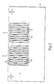
- a method of mounting an electrical component on to a discrete area of a substrate comprising providing said discrete area with a plurality of grooves and securing the component to said area, characterised in that said substrate (1) is insulating and in that said grooves are formerly providing a first conductive layer (2) on the substrate and providing a second conductive layer (3) over the first layer, the second layer forming an evenly distributed series of troughs (4A, 4B, 4C) and lands (3A, 3B, 3C).
- a substrate having for mounting a heat-generating device an area formed with grooves, characterised in that the substrate (1) is insulating and has been formed in a first thick film layer (2) and a second thick film layer (3) on top of the first, the second layer being in the form of an evenly distributed series of troughs (4A, 4B, 4C) and lands (3A, 3B, 3C).
- a ceramic substrate 1 of beryllia or alumina has provided thereon a thick film solder pad comprising a first layer 2 of conductive thick film material such as a material sold by DuPont under their reference number 9923.
- a second thick film layer 3 is provided in a pattern defining a series of ridges 3A, 3B, 3C, 3D etc, evenly spaced with grooves in between, 4A, 4B, 4C etc.
- This layer is made of the same material as the layer 2 and is positioned directly on top of the first layer.
- the ridges are typically 0.5mm wide and the grooves typically 0.15mm wide.
- any voids in the joint are channelled into the grooves which in this embodiment occupy less than 20% of the available surface area of the solder joint interface. This improved solder coverage gives better thermal dissipation and improved mechanical strength. It is to be noted that the invention is not limited to solder bonds but also covers bonds of similar construction made with materials other than those traditionally associated with the thick film circuit technology and solder.
- the materials used for the first and second layers are either copper, palladium, gold, silver, platinum gold, or palladium silver, in any combination.
- the depth of the grooves is typically 0.03mm.
- the groove spacing could be as small as 0.05mm and the percentage of grooves to ridges could be as low as 10%. It is thought unlikely that the percentage of grooves to ridges could exceed 30% and still achieve an acceptable bond.
- Fig. 2 there is shown a circuit layout for a pair of solder pads each similar to the one described in Fig. 1 and wherein here the ceramic substrate 10 has two solder pads 11 and 12 comprising a series of ribs such as 13 made as described with reference to Fig. 1 and insulated from a surrounding conductive area 14 to which connection can be made to the semiconductor devices soldered to the ribs 13 and grooves 13A.
- a typical semiconductor device which would be soldered on to the rib structure would be an MOS power transistor.
Landscapes
- Engineering & Computer Science (AREA)
- Microelectronics & Electronic Packaging (AREA)
- Computer Hardware Design (AREA)
- Power Engineering (AREA)
- Manufacturing & Machinery (AREA)
- Die Bonding (AREA)
- Electric Connection Of Electric Components To Printed Circuits (AREA)
Applications Claiming Priority (2)
| Application Number | Priority Date | Filing Date | Title |
|---|---|---|---|
| GB08620793A GB2194477A (en) | 1986-08-28 | 1986-08-28 | Solder joint |
| GB8620793 | 1986-08-28 |
Publications (2)
| Publication Number | Publication Date |
|---|---|
| EP0259035A2 true EP0259035A2 (de) | 1988-03-09 |
| EP0259035A3 EP0259035A3 (de) | 1989-01-25 |
Family
ID=10603315
Family Applications (1)
| Application Number | Title | Priority Date | Filing Date |
|---|---|---|---|
| EP87307154A Withdrawn EP0259035A3 (de) | 1986-08-28 | 1987-08-13 | Lötverbindung zwischen einem elektrischen Bauelement und einem Substrat |
Country Status (4)
| Country | Link |
|---|---|
| US (1) | US4793543A (de) |
| EP (1) | EP0259035A3 (de) |
| CA (1) | CA1261975A (de) |
| GB (1) | GB2194477A (de) |
Cited By (2)
| Publication number | Priority date | Publication date | Assignee | Title |
|---|---|---|---|---|
| EP0337540B1 (de) * | 1988-04-08 | 1994-10-12 | Koninklijke Philips Electronics N.V. | Gefüge aus einem Träger und einem Halbleiterkörper und Verfahren zum Herstellen desselben |
| CN104332448A (zh) * | 2013-03-05 | 2015-02-04 | 弗莱克斯电子有限责任公司 | 溢出通路 |
Families Citing this family (15)
| Publication number | Priority date | Publication date | Assignee | Title |
|---|---|---|---|---|
| US4851301A (en) * | 1988-02-12 | 1989-07-25 | Motorola, Inc. | Solder bonding with improved peel strength |
| AT394331B (de) * | 1990-09-21 | 1992-03-10 | Plansee Metallwerk | Verfahren zur herstellung hochfester loetverbindungen |
| US5369880A (en) * | 1993-05-06 | 1994-12-06 | Motorola, Inc. | Method for forming solder deposit on a substrate |
| US5488013A (en) * | 1993-12-20 | 1996-01-30 | International Business Machines Corporation | Method of forming transverse diffusion barrier interconnect structure |
| US5906310A (en) * | 1994-11-10 | 1999-05-25 | Vlt Corporation | Packaging electrical circuits |
| JP2732823B2 (ja) * | 1995-02-02 | 1998-03-30 | ヴィエルティー コーポレーション | はんだ付け方法 |
| US6090643A (en) | 1998-08-17 | 2000-07-18 | Teccor Electronics, L.P. | Semiconductor chip-substrate attachment structure |
| US6316737B1 (en) | 1999-09-09 | 2001-11-13 | Vlt Corporation | Making a connection between a component and a circuit board |
| DE10010979A1 (de) * | 2000-03-07 | 2001-09-13 | Bosch Gmbh Robert | Elektrische Schaltung und Substrat hierzu |
| US6985341B2 (en) | 2001-04-24 | 2006-01-10 | Vlt, Inc. | Components having actively controlled circuit elements |
| US7443229B1 (en) | 2001-04-24 | 2008-10-28 | Picor Corporation | Active filtering |
| EP1284590A1 (de) * | 2001-08-14 | 2003-02-19 | Swissvoice AG | Vorrichtungen zur Kontaktierung von Anschlussleitungen mittels eines eleastischen, geschichteten Verbindungselementes |
| WO2008132559A1 (en) * | 2007-04-27 | 2008-11-06 | Freescale Semiconductor, Inc. | Semiconductor wafer processing |
| US8466548B2 (en) * | 2011-05-31 | 2013-06-18 | Infineon Technologies Ag | Semiconductor device including excess solder |
| JP6072667B2 (ja) * | 2013-11-12 | 2017-02-01 | 三菱電機株式会社 | 半導体モジュールとその製造方法 |
Family Cites Families (8)
| Publication number | Priority date | Publication date | Assignee | Title |
|---|---|---|---|---|
| US3860949A (en) * | 1973-09-12 | 1975-01-14 | Rca Corp | Semiconductor mounting devices made by soldering flat surfaces to each other |
| SU538834A1 (ru) * | 1974-08-27 | 1976-12-15 | Предприятие П/Я Х-5885 | Способ пайки разнородных материалов |
| US3934336A (en) * | 1975-01-13 | 1976-01-27 | Burroughs Corporation | Electronic package assembly with capillary bridging connection |
| US4413766A (en) * | 1981-04-03 | 1983-11-08 | General Electric Company | Method of forming a conductor pattern including fine conductor runs on a ceramic substrate |
| US4409278A (en) * | 1981-04-16 | 1983-10-11 | General Electric Company | Blister-free direct bonding of metals to ceramics and metals |
| JPS59150453A (ja) * | 1982-12-23 | 1984-08-28 | Toshiba Corp | 半導体モジユ−ル用基板の製造方法 |
| SU1215908A1 (ru) * | 1984-07-13 | 1986-03-07 | Новосибирский электротехнический институт | Способ пайки деталей из разнородных материалов |
| DE3442537A1 (de) * | 1984-11-22 | 1986-05-22 | BBC Aktiengesellschaft Brown, Boveri & Cie., Baden, Aargau | Verfahren zum blasenfreien verbinden eines grossflaechigen halbleiter-bauelements mit einem als substrat dienenden bauteil mittels loeten |
-
1986
- 1986-08-28 GB GB08620793A patent/GB2194477A/en not_active Withdrawn
-
1987
- 1987-08-13 EP EP87307154A patent/EP0259035A3/de not_active Withdrawn
- 1987-08-26 CA CA000545373A patent/CA1261975A/en not_active Expired
- 1987-08-28 US US07/091,054 patent/US4793543A/en not_active Expired - Fee Related
Cited By (3)
| Publication number | Priority date | Publication date | Assignee | Title |
|---|---|---|---|---|
| EP0337540B1 (de) * | 1988-04-08 | 1994-10-12 | Koninklijke Philips Electronics N.V. | Gefüge aus einem Träger und einem Halbleiterkörper und Verfahren zum Herstellen desselben |
| CN104332448A (zh) * | 2013-03-05 | 2015-02-04 | 弗莱克斯电子有限责任公司 | 溢出通路 |
| CN104332448B (zh) * | 2013-03-05 | 2018-12-04 | 弗莱克斯电子有限责任公司 | 溢出通路 |
Also Published As
| Publication number | Publication date |
|---|---|
| EP0259035A3 (de) | 1989-01-25 |
| GB2194477A (en) | 1988-03-09 |
| US4793543A (en) | 1988-12-27 |
| CA1261975A (en) | 1989-09-26 |
| GB8620793D0 (en) | 1986-10-08 |
Similar Documents
| Publication | Publication Date | Title |
|---|---|---|
| US4793543A (en) | Solder joint | |
| EP1416533B1 (de) | Leistungshalbleiter und Aluminium-direktgebondetes Substrat dafür | |
| US5650662A (en) | Direct bonded heat spreader | |
| US4556899A (en) | Insulated type semiconductor devices | |
| US5465898A (en) | Process for producing a metal-ceramic substrate | |
| JP3333409B2 (ja) | 半導体モジュール | |
| JPH07202063A (ja) | セラミックス回路基板 | |
| US3675089A (en) | Heat dispenser from a semiconductor wafer by a multiplicity of unaligned minuscule heat conductive raised dots | |
| KR970024069A (ko) | 반도체장치 및 그 제조방법(semiconductor device and method of manufacturing semiconductor device) | |
| EP0935286A4 (de) | Kupfer-schaltungsverbindungssubstrat und seine herstellung | |
| US6115255A (en) | Hybrid high-power integrated circuit | |
| US7193318B2 (en) | Multiple power density chip structure | |
| JPH05259328A (ja) | 半導体モジュール | |
| EP0812015A1 (de) | Kühlkörper für integrierte Schaltungen | |
| JP2002299495A (ja) | 半導体回路基板 | |
| JP2005011922A (ja) | ヒートシンクを備えた両面銅貼り基板、およびこれを用いた半導体装置 | |
| US6483706B2 (en) | Heat dissipation for electronic components | |
| US5866951A (en) | Hybrid circuit with an electrically conductive adhesive | |
| US6529379B1 (en) | Article exhibiting enhanced adhesion between a dielectric substrate and heat spreader and method | |
| JP3139523B2 (ja) | 放熱フィン | |
| US6175148B1 (en) | Electrical connection for a power semiconductor component | |
| JP3588315B2 (ja) | 半導体素子モジュール | |
| WO2020201005A1 (en) | Semiconductor module and method for manufacturing it | |
| JP2521624Y2 (ja) | 半導体装置 | |
| JP2001135753A (ja) | 半導体モジュール用基板及びその製造方法 |
Legal Events
| Date | Code | Title | Description |
|---|---|---|---|
| PUAI | Public reference made under article 153(3) epc to a published international application that has entered the european phase |
Free format text: ORIGINAL CODE: 0009012 |
|
| AK | Designated contracting states |
Kind code of ref document: A2 Designated state(s): BE DE FR IT NL SE |
|
| PUAL | Search report despatched |
Free format text: ORIGINAL CODE: 0009013 |
|
| AK | Designated contracting states |
Kind code of ref document: A3 Designated state(s): BE DE FR IT NL SE |
|
| 17P | Request for examination filed |
Effective date: 19890208 |
|
| STAA | Information on the status of an ep patent application or granted ep patent |
Free format text: STATUS: THE APPLICATION IS DEEMED TO BE WITHDRAWN |
|
| 18D | Application deemed to be withdrawn |
Effective date: 19910301 |
|
| RIN1 | Information on inventor provided before grant (corrected) |
Inventor name: JONES, ALAN ROBERT Inventor name: GAINEY, TREVOR CLIFFORD Inventor name: HALL, IAN |