EP0258975A2 - Taktbussystem für eine integrierte Schaltung - Google Patents
Taktbussystem für eine integrierte Schaltung Download PDFInfo
- Publication number
- EP0258975A2 EP0258975A2 EP87305816A EP87305816A EP0258975A2 EP 0258975 A2 EP0258975 A2 EP 0258975A2 EP 87305816 A EP87305816 A EP 87305816A EP 87305816 A EP87305816 A EP 87305816A EP 0258975 A2 EP0258975 A2 EP 0258975A2
- Authority
- EP
- European Patent Office
- Prior art keywords
- clock
- conductor
- clock bus
- distribution leg
- delay
- Prior art date
- Legal status (The legal status is an assumption and is not a legal conclusion. Google has not performed a legal analysis and makes no representation as to the accuracy of the status listed.)
- Withdrawn
Links
Images
Classifications
-
- G—PHYSICS
- G06—COMPUTING OR CALCULATING; COUNTING
- G06F—ELECTRIC DIGITAL DATA PROCESSING
- G06F1/00—Details not covered by groups G06F3/00 - G06F13/00 and G06F21/00
- G06F1/04—Generating or distributing clock signals or signals derived directly therefrom
- G06F1/10—Distribution of clock signals, e.g. skew
-
- G—PHYSICS
- G06—COMPUTING OR CALCULATING; COUNTING
- G06F—ELECTRIC DIGITAL DATA PROCESSING
- G06F1/00—Details not covered by groups G06F3/00 - G06F13/00 and G06F21/00
- G06F1/04—Generating or distributing clock signals or signals derived directly therefrom
Definitions
- the present invention is a clock bus system for use on very large-scale integrated (VLSI) circuits.
- VLSI very large-scale integrated
- Modern digital computers are formed by hundreds of thousands and even millions of logic elements.
- these logic elements are fabricated on very large-scale integrated (VLSI) circuit chips known as gate arrays.
- VLSI very large-scale integrated
- the gate arrays themselves are organized onto a plurality of major function circuit boards which are dedicated to the performance of specific tasks.
- a supercomputer for example, can include a central processing unit (CPU), memory interface, and input/output (I/O) major function circuit boards. Each of these circuit boards will typically be formed by hundreds of gate arrays.
- the computer includes a central clock distribution system for providing a clock signal in the form of a synchronized train of clock pulses to all gate arrays.
- a clock system of this type is disclosed in an application entitled “Electronic Clock Tuning System", Serial No. 06/8l4,654, filed December 30, l985, and assigned to the same assignee as the present invention.
- each gate array distributes the clock signal to each individual circuit element. For the very same reasons that each gate array must receive synchronized clock signals from the central clock distribution system, it is imperative that each circuit element on the gate array receive a synchronized train of clock pulses from the clock bus system.
- Frequency of the clock pulse train is limited by the uncertainty, or maximum skew, introduced between clock pulse trains supplied to various circuit elements on the gate array. Simply put, computer performance can be greatly increased by reducing skews introduced by the clock bus system.
- the clock signal is branched out to all circuit elements on the gate array through a tree-type network formed by a plurality of buffers.
- the network is made large enough to provide a clock signal to each circuit element which requires it.
- Still another prior art clock bus structure includes a clock bus which circumscribes all circuit elements on the gate array. Although this clock bus structure permits shorter interconnections between the clock bus and individual circuit elements, delays are introduced by the clock bus itself.
- the present invention is a clock bus system for distributing a train of clock pulses to a plurality of circuit elements.
- a train of clock pulses is received by input means.
- Clock bus means for propagating the train of clock pulses substantially circumscribe the circuit elements.
- Each circuit element is coupled to the clock bus means.
- a plurality of distribution leg means are coupled to the input means by conductors, and provide the train of clock pulses to the clock bus means at spaced-apart locations.
- the clock bus system is fabricated on an integrated circuit.
- Each distribution leg means also includes a clock bus driver.
- the conductors which couple the distribution leg means to the input means delay the clock pulse train by conductor delay periods, and at least some of the conductor delay periods differ.
- At least some of the distribution leg means include delay means for delaying the clock pulse trains by predetermined time periods. The predetermined time periods of the delay means of each distribution leg correspond to a difference between a greatest conductor delay period, and the conductor delay period of the particular distribution leg means.
- the clock bus system is well suited for fabrication on very large-scale integrated circuits used as components of supercomputers. Since the clock bus circumscribes all circuit elements, it can be coupled to the circuit elements by conductors of relatively uniform length, thereby reducing clock bus-to-circuit element skews. The clock bus is also driven at several spaced-apart locations by synchronized clock pulse trains. Skews introduced by the clock bus itself are therefore reduced increasing overall computer performance.
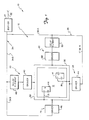
- Figure l is a block diagram representation of the clock bus system of the present invention.
- FIG. l An integrated circuit l0 which includes clock bus system l2 of the present invention is illustrated generally in Figure l.
- a plurality of circuit elements l4 flip-flops are shown for purposes of example) are fabricated on a main body portion l8 of integrated circuit l0 in accordance with any known circuit technology.
- clock bus system l2 is fabricated on a 20K CMOS gate array.
- Clock bus system l2 includes buffer l9, a plurality of distribution legs 20, 22, 24, and 26, and clock bus 30.
- Clock bus system l0 provides synchronized system clock signals in the form of trains of clock pulses to circuit elements l4.
- Clock bus 30 is a conductor such as metal foil which substantially surrounds, or circumscribes, all circuit elements l4 which require a system clock signal.
- clock bus 30 is rectangular in shape, closed, and completely circumscribes body portion l8 of integrated circuit l0.
- Clock bus 30 has an extended length, and is typically positioned near the periphery of integrated circuit l0.
- Clock bus 30 need only provide a convenient point of interconnection to circuit elements from several sides of body portion l8.
- circuit elements l4 on integrated circuit l0 which require a system clock signal have their clock terminal (indicated by a sideways "v" on the flip-flops) coupled to receive the system clock signal from clock bus 30 by conductors 3l. Since clock bus 30 circumscribes circuit elements l4, they are all physically located near at least one side of clock bus 30. Short conductors 3l of relatively uniform length can therefore be used to interconnect circuit elements l4 to clock bus 30. Skews introduced by conductors 3l are thereby kept to a minimum.
- a train of clock pulses provided by a central clock distribution system such as that described in an application entitled "Electronic Clock Tuning System", Serial No. 06/8l4,654, which is assigned to the same assignee as the present invention, is coupled to integrated circuit l0 through input terminal 32 and applied to buffer l9.
- Buffer l9 isolates other elements of clock bus system l2 from the central clock distribution system.
- Distribution legs 20, 22, 24, and 26 are coupled to receive the clock pulse train from buffer l9, and supply the clock pulse train to clock bus 30 at several spaced-apart locations.
- the clock pulse train is coupled to distribution legs 20 and 26 by conductor 34, with conductor section 34A interconnecting buffer l9 and distribution leg 20, and conductor section 34B coupling conductor section 34A to distribution leg 26.
- conductor 36 has a first section 36A which couples buffer l9 to distribution leg 22, and a second section 36B which interconnects conductor section 36A to distribution leg 24.
- distribution legs 20, 22, 24, and 26 each supply the clock pulse train to points on clock bus 30 which are equidistant from one another, and spaced ninety degrees apart.
- Distribution legs 20, 22, 24 and 26 preferably include drivers 40, 42, 44, and 46, respectively.
- Drivers 40-46 are common circuit elements which convert the electrical characteristics of the clock pulse train received from buffer l9 to those required to drive all circuit elements l4 on integrated circuit l0.
- drivers 40-46 are programmable devices, the load drive capability of which can be adjusted depending upon whether clock bus 30 is heavily or lightly loaded by circuit elements l4.
- distribution legs 20, 22, 24, and 26 and buffer l9 differs since some of these distribution legs are located on integrated circuit l0 at points more distant from buffer l9 than others.
- Clock pulses which are provided to distribution leg 26, for example must be propagated through conductor sections 34A and 34B, while the clock pulses provided to distribution leg 20 are propagated only through conductor section 34A.
- the clock pulse trains supplied to clock bus 30 through distribution legs 24 and 26 would be skewed with respect to those provided by distribution legs 20 and 22.
- at least some of distribution legs 20, 22, 24 and 26 of clock bus system l2 include delay elements to insure minimum skew between the clock pulse trains provided by these distribution legs to clock bus 30.
- conductor sections 34A and 36A are fabricated in such a manner that they have nearly identical lengths.
- the clock pulse trains provided to by distribution legs 20 and 22 will therefore both be delayed by the same amount of time, and be synchronized with respect to each other.
- Conductor sections 34B and 36B are also nearly identical in length.
- the clock pulse trains provided to distribution legs 24 and 26 will also be synchronized with respect to each other, although these clock pulse trains will be skewed with respect to those provided to distribution legs 20 and 22 due to the additional propagation delay of conductor sections 34B and 36B.
- distribution legs 20 and 22 include delay elements 48 and 50, respectively.
- Delay elements 48 and 50 delay the clock pulse trains provided to clock bus 30 by distribution legs 20 and 22, respectively, by a delay period equal to the propagation delay, or conductor delay period, of conductor sections 34B and 36B.
- Delay elements 48 and 50 therefore delay the clock pulse trains provided to distribution legs 20 and 22, respectively, by time periods corresponding to a difference between the delay imposed by the longest conductor (both sections A and B of conductors 34 and 36) and the delay imposed by conductor sections 34A and 36B which couple distribution legs 20 and 22, respectively, to buffer l9.
- delay elements 48 and 50 are comprised of resistors which together with the input capacitance of drivers 40 and 42, respectively, function as RC networks and delay the clock pulse trains by the desired period.
- the clock pulse trains provided to clock bus 30 by distribution legs 20-26 will therefore all be synchronized with respect to each other.
- delay elements 48 and 50 both delay the clock pulse train received thereby by approximately 300 picoseconds to compensate for the propagation delay of conductor sections 34B and 36B, respectively.
- Skews between clock pulse trains provided to clock bus 30 by distribution legs 20-26 can be kept to within 200 picoseconds.
- Skews between clock bus 30 and circuit elements l4 caused by conductors 3l can be kept to within 200-300 picoseconds.
- skews between the clock pulse trains provided to circuit elements l4 can be reduced to 400-500 picoseconds using clock bus system l2. This is an improvement of 600-l200 picoseconds over that of prior art techniques implemented on an integrated circuit with a similar clock frequency. This improvement amounts to approximately 5%-l0% of the system clock period.
Landscapes
- Engineering & Computer Science (AREA)
- Theoretical Computer Science (AREA)
- Physics & Mathematics (AREA)
- General Engineering & Computer Science (AREA)
- General Physics & Mathematics (AREA)
- Semiconductor Integrated Circuits (AREA)
- Design And Manufacture Of Integrated Circuits (AREA)
- Information Transfer Systems (AREA)
- Manipulation Of Pulses (AREA)
Applications Claiming Priority (2)
| Application Number | Priority Date | Filing Date | Title |
|---|---|---|---|
| US883829 | 1986-07-09 | ||
| US06/883,829 US4769558A (en) | 1986-07-09 | 1986-07-09 | Integrated circuit clock bus layout delay system |
Publications (2)
| Publication Number | Publication Date |
|---|---|
| EP0258975A2 true EP0258975A2 (de) | 1988-03-09 |
| EP0258975A3 EP0258975A3 (de) | 1989-07-12 |
Family
ID=25383413
Family Applications (1)
| Application Number | Title | Priority Date | Filing Date |
|---|---|---|---|
| EP87305816A Withdrawn EP0258975A3 (de) | 1986-07-09 | 1987-07-01 | Taktbussystem für eine integrierte Schaltung |
Country Status (5)
| Country | Link |
|---|---|
| US (1) | US4769558A (de) |
| EP (1) | EP0258975A3 (de) |
| JP (1) | JPS6341918A (de) |
| AU (1) | AU589789B2 (de) |
| CA (1) | CA1271988A (de) |
Cited By (3)
| Publication number | Priority date | Publication date | Assignee | Title |
|---|---|---|---|---|
| EP0355769A3 (en) * | 1988-08-19 | 1990-06-06 | Kabushiki Kaisha Toshiba | Clock supply circuit clock supply circuit |
| EP0451079A3 (en) * | 1990-03-30 | 1992-03-25 | International Business Machines Corporation | Reducing clock skew in large-scale integrated circuits |
| EP1383025A3 (de) * | 2002-06-12 | 2004-11-10 | Nec Corporation | Integrierte Schaltunganordnung mit reduzierter Taktverschiebung |
Families Citing this family (16)
| Publication number | Priority date | Publication date | Assignee | Title |
|---|---|---|---|---|
| US5291043A (en) * | 1990-02-07 | 1994-03-01 | Mitsubishi Denki Kabushiki Kaisha | Semiconductor integrated circuit device having gate array |
| JP2507677B2 (ja) * | 1990-06-28 | 1996-06-12 | 富士通株式会社 | 分散型デ―タ処理装置 |
| JP3026387B2 (ja) * | 1991-08-23 | 2000-03-27 | 沖電気工業株式会社 | 半導体集積回路 |
| JP3048471B2 (ja) * | 1992-09-08 | 2000-06-05 | 沖電気工業株式会社 | クロック供給回路及びクロックスキュー調整方法 |
| US5467033A (en) * | 1993-07-02 | 1995-11-14 | Tandem Computers Incorporated | Chip clock skew control method and apparatus |
| US5448208A (en) * | 1993-07-15 | 1995-09-05 | Nec Corporation | Semiconductor integrated circuit having an equal propagation delay |
| JPH0737990A (ja) * | 1993-07-16 | 1995-02-07 | Nec Corp | クロック分配方式 |
| US5481209A (en) * | 1993-09-20 | 1996-01-02 | Lsi Logic Corporation | Clock distribution and control in an integrated circuit |
| JP3112784B2 (ja) * | 1993-09-24 | 2000-11-27 | 日本電気株式会社 | クロック信号分配回路 |
| US5652529A (en) * | 1995-06-02 | 1997-07-29 | International Business Machines Corporation | Programmable array clock/reset resource |
| US5570045A (en) * | 1995-06-07 | 1996-10-29 | Lsi Logic Corporation | Hierarchical clock distribution system and method |
| US5717229A (en) * | 1996-03-26 | 1998-02-10 | Intel Corporation | Method and apparatus for routing a clock tree in an integrated circuit package |
| US6305001B1 (en) * | 1998-06-18 | 2001-10-16 | Lsi Logic Corporation | Clock distribution network planning and method therefor |
| US6513149B1 (en) | 2000-03-31 | 2003-01-28 | International Business Machines Corporation | Routing balanced clock signals |
| KR100338779B1 (ko) | 2000-08-28 | 2002-05-31 | 윤종용 | 버스라인들 간의 스큐를 방지하기 위한 메모리 모듈 |
| US7622965B2 (en) * | 2006-01-31 | 2009-11-24 | International Business Machines Corporation | Dual-edge shaping latch/synchronizer for re-aligning edges |
Family Cites Families (21)
| Publication number | Priority date | Publication date | Assignee | Title |
|---|---|---|---|---|
| US3171981A (en) * | 1962-07-02 | 1965-03-02 | Ibm | Clock pulse generation and distribution circuit |
| US3418498A (en) * | 1965-10-29 | 1968-12-24 | Westinghouse Electric Corp | Delay line timing circuit for use with computer or other timed operation devices |
| US3633113A (en) * | 1969-12-22 | 1972-01-04 | Ibm | Timed pulse train generating system |
| US3725793A (en) * | 1971-12-15 | 1973-04-03 | Bell Telephone Labor Inc | Clock synchronization arrangement employing delay devices |
| US3753012A (en) * | 1972-02-17 | 1973-08-14 | Motorola Inc | Circuit for providing precise time delay |
| US4208724A (en) * | 1977-10-17 | 1980-06-17 | Sperry Corporation | System and method for clocking data between a remote unit and a local unit |
| US4241418A (en) * | 1977-11-23 | 1980-12-23 | Honeywell Information Systems Inc. | Clock system having a dynamically selectable clock period |
| DE2853523C2 (de) * | 1978-12-12 | 1981-10-01 | Ibm Deutschland Gmbh, 7000 Stuttgart | Dezentrale Erzeugung von Taktsteuersignalen |
| US4321687A (en) * | 1979-10-01 | 1982-03-23 | International Business Machines Corporation | Timing pulse generation |
| US4414637A (en) * | 1981-01-13 | 1983-11-08 | Honeywell Information Systems Inc. | Adjustable clock system having a dynamically selectable clock period |
| US4447876A (en) * | 1981-07-30 | 1984-05-08 | Tektronix, Inc. | Emulator control sequencer |
| JPS5835963A (ja) * | 1981-08-28 | 1983-03-02 | Fujitsu Ltd | 集積回路装置 |
| JPS58101525A (ja) * | 1981-12-14 | 1983-06-16 | Fujitsu Ltd | 論理回路 |
| US4412342A (en) * | 1981-12-18 | 1983-10-25 | Gte Automatic Electric Labs Inc. | Clock synchronization system |
| US4482826A (en) * | 1982-02-16 | 1984-11-13 | Lecroy Research Systems Corporation | Programmable delay device |
| DE3211595A1 (de) * | 1982-03-30 | 1983-10-06 | Gewerk Eisenhuette Westfalia | Bruch- und versatzabschirmung eines lemniskatenschildes |
| US4479216A (en) * | 1982-12-22 | 1984-10-23 | At&T Bell Laboratories | Skew-free clock circuit for integrated circuit chip |
| JPS59190022A (ja) * | 1983-04-11 | 1984-10-27 | Mitsui Mining & Smelting Co Ltd | 自動車における換気窓用覆蓋のロツク装置 |
| US4639615A (en) * | 1983-12-28 | 1987-01-27 | At&T Bell Laboratories | Trimmable loading elements to control clock skew |
| EP0173521A3 (de) * | 1984-08-29 | 1988-05-11 | Unisys Corporation | Gerät zur automatischen Angleichung von Signalverzögerungen |
| JPS6182525A (ja) * | 1984-09-29 | 1986-04-26 | Toshiba Corp | 半導体集積回路装置 |
-
1986
- 1986-07-09 US US06/883,829 patent/US4769558A/en not_active Expired - Lifetime
-
1987
- 1987-06-24 CA CA000541046A patent/CA1271988A/en not_active Expired - Fee Related
- 1987-07-01 EP EP87305816A patent/EP0258975A3/de not_active Withdrawn
- 1987-07-07 AU AU75290/87A patent/AU589789B2/en not_active Ceased
- 1987-07-09 JP JP62172036A patent/JPS6341918A/ja active Pending
Cited By (5)
| Publication number | Priority date | Publication date | Assignee | Title |
|---|---|---|---|---|
| EP0355769A3 (en) * | 1988-08-19 | 1990-06-06 | Kabushiki Kaisha Toshiba | Clock supply circuit clock supply circuit |
| US5013942A (en) * | 1988-08-19 | 1991-05-07 | Kabushiki Kaisha Toshiba | Clock supply circuit having adjustment capacitance |
| EP0451079A3 (en) * | 1990-03-30 | 1992-03-25 | International Business Machines Corporation | Reducing clock skew in large-scale integrated circuits |
| EP1383025A3 (de) * | 2002-06-12 | 2004-11-10 | Nec Corporation | Integrierte Schaltunganordnung mit reduzierter Taktverschiebung |
| US7005907B2 (en) | 2002-06-12 | 2006-02-28 | Nec Corporation | Integrated circuit device with clock skew reduced |
Also Published As
| Publication number | Publication date |
|---|---|
| EP0258975A3 (de) | 1989-07-12 |
| US4769558A (en) | 1988-09-06 |
| AU589789B2 (en) | 1989-10-19 |
| JPS6341918A (ja) | 1988-02-23 |
| CA1271988A (en) | 1990-07-24 |
| AU7529087A (en) | 1988-01-14 |
Similar Documents
| Publication | Publication Date | Title |
|---|---|---|
| US4769558A (en) | Integrated circuit clock bus layout delay system | |
| US5696949A (en) | System for PCI slots expansion using asynchronous PCI-to-PCI bridge with clock generator for providing clock signal to the expansion mother board and expansion side of bridge | |
| US5546023A (en) | Daisy chained clock distribution scheme | |
| US5461332A (en) | Multiple frequency output clock generator system | |
| US5712883A (en) | Clock signal distribution system | |
| US5296748A (en) | Clock distribution system | |
| US5086427A (en) | Clocked logic circuitry preventing double driving on shared data bus | |
| EP0362691A3 (de) | Verteilungseinrichtung für phasenverschiebungsfreie Taktsignale | |
| US3745472A (en) | Synchronous digital system having a clock distribution system | |
| US4839604A (en) | Integrated circuit with clock distribution means for supplying clock signals | |
| US6255878B1 (en) | Dual path asynchronous delay circuit | |
| US5767718A (en) | High speed conditional synchronous one shot circuit | |
| EP0632358B1 (de) | Verfahren und Vorrichtung zur Steuerung der Auf-dem-Chip-Taktverschiebung | |
| US5994924A (en) | Clock distribution network with dual wire routing | |
| US6005428A (en) | System and method for multiple chip self-aligning clock distribution | |
| US6587907B1 (en) | System and method for generating a clock delay within an interconnect cable assembly | |
| US6172528B1 (en) | Charge sharing circuit for fanout buffer | |
| US5771372A (en) | Apparatus for delaying the output of data onto a system bus | |
| US20060031697A1 (en) | Method and system for reducing the effects of simultaneously switching outputs | |
| US4918331A (en) | Logic circuits with data resynchronization | |
| US6144224A (en) | Clock distribution network with dual wire routing | |
| US5303365A (en) | Clock generation in a multi-chip computer system | |
| US6590795B2 (en) | High speed data capture circuit for a digital device | |
| US7328361B2 (en) | Digital bus synchronizer for generating read reset signal | |
| US3084286A (en) | Binary counter |
Legal Events
| Date | Code | Title | Description |
|---|---|---|---|
| PUAI | Public reference made under article 153(3) epc to a published international application that has entered the european phase |
Free format text: ORIGINAL CODE: 0009012 |
|
| AK | Designated contracting states |
Kind code of ref document: A2 Designated state(s): AT BE CH DE ES FR GB GR IT LI LU NL SE |
|
| PUAL | Search report despatched |
Free format text: ORIGINAL CODE: 0009013 |
|
| AK | Designated contracting states |
Kind code of ref document: A3 Designated state(s): AT BE CH DE ES FR GB GR IT LI LU NL SE |
|
| STAA | Information on the status of an ep patent application or granted ep patent |
Free format text: STATUS: THE APPLICATION IS DEEMED TO BE WITHDRAWN |
|
| 18D | Application deemed to be withdrawn |
Effective date: 19900113 |
|
| RIN1 | Information on inventor provided before grant (corrected) |
Inventor name: BACH, RANDALL E. |