EP0257971A2 - Tampon à hystérésis compensé en température - Google Patents
Tampon à hystérésis compensé en température Download PDFInfo
- Publication number
- EP0257971A2 EP0257971A2 EP87307320A EP87307320A EP0257971A2 EP 0257971 A2 EP0257971 A2 EP 0257971A2 EP 87307320 A EP87307320 A EP 87307320A EP 87307320 A EP87307320 A EP 87307320A EP 0257971 A2 EP0257971 A2 EP 0257971A2
- Authority
- EP
- European Patent Office
- Prior art keywords
- hysteresis
- set forth
- input signal
- buffer
- circuit
- Prior art date
- Legal status (The legal status is an assumption and is not a legal conclusion. Google has not performed a legal analysis and makes no representation as to the accuracy of the status listed.)
- Granted
Links
- 239000000872 buffer Substances 0.000 title claims description 35
- 238000000034 method Methods 0.000 claims description 19
- 230000001902 propagating effect Effects 0.000 claims 3
- 239000004065 semiconductor Substances 0.000 claims 2
- 230000008878 coupling Effects 0.000 claims 1
- 238000010168 coupling process Methods 0.000 claims 1
- 238000005859 coupling reaction Methods 0.000 claims 1
- 230000000644 propagated effect Effects 0.000 abstract description 6
- 238000004519 manufacturing process Methods 0.000 abstract description 4
- 230000001419 dependent effect Effects 0.000 description 4
- 238000010586 diagram Methods 0.000 description 3
- 238000012986 modification Methods 0.000 description 2
- 230000004048 modification Effects 0.000 description 2
- 238000004458 analytical method Methods 0.000 description 1
- 230000003466 anti-cipated effect Effects 0.000 description 1
- 238000004364 calculation method Methods 0.000 description 1
- 230000000694 effects Effects 0.000 description 1
- 238000010348 incorporation Methods 0.000 description 1
- 230000000630 rising effect Effects 0.000 description 1
- 230000001960 triggered effect Effects 0.000 description 1
Images
Classifications
-
- H—ELECTRICITY
- H03—ELECTRONIC CIRCUITRY
- H03K—PULSE TECHNIQUE
- H03K3/00—Circuits for generating electric pulses; Monostable, bistable or multistable circuits
- H03K3/02—Generators characterised by the type of circuit or by the means used for producing pulses
- H03K3/027—Generators characterised by the type of circuit or by the means used for producing pulses by the use of logic circuits, with internal or external positive feedback
- H03K3/037—Bistable circuits
- H03K3/0377—Bistables with hysteresis, e.g. Schmitt trigger
-
- H—ELECTRICITY
- H03—ELECTRONIC CIRCUITRY
- H03K—PULSE TECHNIQUE
- H03K3/00—Circuits for generating electric pulses; Monostable, bistable or multistable circuits
- H03K3/01—Details
- H03K3/011—Modifications of generator to compensate for variations in physical values, e.g. voltage, temperature
Definitions
- the invention generally relates to hysteresis circuits we will describe to high-speed temperature compensated hysteresis circuits which guarantee a predetermined minimum hysteresis window over a wide temperature range so that the circuits are suitable for use in military applications and hostile environments.
- Hysteresis circuits are well known devices for accurately detecting a change in the value of an input signal voltage. These circuits operate by varying threshold voltage values so that when the input signal value is "low", a high threshold, V IH , is set and when the input signal is "high” a low threshold value V IL is set.
- V IH a high threshold
- V IL a low threshold value
- hysteresis circuits are not output independent.
- signals output by a hysteresis circuit are also fed back to the circuit itself to set up the hysteresis reference levels (the threshold voltages V IL and V IH ).
- the hysteresis reference levels may be affected by variables in the output stage, for example, output current. It would therefore be desirable to have a hysteresis circuit which operates in parallel with data being propagated to the output stage, independent of the output itself, to eliminate such variables.
- hysteresis circuits having all the features set forth herein strictlybefore assure a minimum preselected hysteresis window over wide temperature ranges.
- this feature is desirable over the 200°C operating range between -55°C and 155°C typically required for military applications. This assurance that a minimum preselected hysteresis window can be guaranteed over a wide temperature range would allow for the incorporation of these circuits in hostile environments generally. Known hysteresis circuits simply do not have this capability.
- a hysteresis circuit in which a first signal path, including a hysteresis feedback loop, is separate from a second signal path that is used to carry data.
- the signal input to the hysteresis circuit also referred to hereinafter as the "input signal” crosses a first preselected hysteresis reference (or “threshold”) level
- the hysteresis feedback loop which includes threshold adjustments means, will cause a change in the threshold from the first preselected level to a second preselected level. This adjustment of threshold level will take place in parallel with the data being propagated to the output over said separate second signal path.
- a subsequent crossing of the second preselected threshold level by said input signal will cause the first threshold level to be reset and so on.
- the threshold adjustment means included in said first signal path further includes a temperature compensation string, current switching means and means which act as an anti-hysteresis killer to speed up the operation of the hysteresis circuit.
- This novel combination is operative to assure a preselected minimum hysteresis window over the 200°C temperature range between -55°C and 155°C, and renders the hysteresis circuit suitable for use in both military applications and other hostile environments.
- the hysteresis circuit has a PNP input stage to reduce I IL and accordingly improve the input characteristics of the circuit, particularly fan-in.
- the circuit also features a low I CC and is designed to be self-compensating with respect to manufacturing disparities inherent in components used to fabricate the circuit itself.
- hysteresis circuit which is capable of adjusting its hysteresis reference level in parallel with data being propagated to the output of the circuit.
- hysteresis circuit that guarantees a minimum preselected hysteresis window over a wide temperature range.
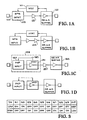
- FIG. 1a a typical prior art hysteresis buffer, 101, is shown in combination with a 48 milliamp output buffer, 102, NPN input stage 103 and buffer 125.
- This circuit arrangement is operative to invert the signal input on line 120.
- An analagous circuit arrangement that does not invert the input is depicted in FIG. 1b.
- the only difference between the circuit depicted in FIG. 1a and FIG. 1b is the inclusion of inverter 104 in the FIG. 1b circuit.
- the hysteresis feedback loop is not separate from the data path.
- the threshold values, V IL and V IH may be affected by variables in the output stage such as output current.
- the hysteresis window defined herein as the difference between V IL and V IH over the operating temperature range of the hysteresis circuit, is dependent on current delivered to the load via output buffer 102.
- the hysteresis window is inherently a function of temperature.
- the hysteresis window of the known circuit arrangements varies considerably with temperature. This is because temperature sensitive components, such as Schotky diodes, are typically used to fabricate the circuits. As a result, not only the load, but swings in temperature as well, will have a significant impact on the degree to which the hysteresis window of known circuits will vary. In short, the known circuits are unreliable at best, if not altogether useless, in situations where widely varying loads and temperatures are present.
- FIGS. 1a and 1b suffer a time delay before a threshold level can be changed. This is because the hysteresis feedback loop is output dependent. Any required switching follows the output serially.
- FIGS. 1c and 1d are presented, in block diagram form, to depict hysteresis buffer circuits arranged according to the preferred embodiment of the invention.
- a PNP input stage, 180 replaces the NPN input stage of the prior art circuit. This will reduce I IL and improve the circuits input characteristics.
- FIG. 1c also depicts hysteresis buffer circuitry 181 with a first signal path, 185, being fedback to the PNP input stage 180 and a second separate signal path, path 186, being used to couple data (via inverter 187) to output buffer 188.
- FIG. 1d is the same as FIG. 1c, except that a noninverter circuit arrangement is shown.
- the separate feedback and data paths shown in FIGS. 1c and 1d speed up switching the threshold levels in the novel circuits. Less time delay is suffered in switching hysteresis reference levels since the switching takes place in parallel with data being propagated to the output stage.
- the separate paths for data and for signals to control the hysteresis reference levels climinates the problem of having the threshold levels being affected by variables in the output stage. It will be demonstrated, with reference to FIG. 2, that a minimum predetermined hysteresis window is guaranteed over wide termperature ranges using the temperature compensation and current switching techniques taught hereinafter.
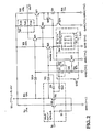
- FIG. 2 depicts the circuit details of a hysteresis buffer that functions as an inverter.
- the circuitry depicted in FIG. 2 corresponds to the functional block 199 shown in dashed lines in FIG. 1c.
- the example set forth hereinafter, for constructing the FIG. 1c inverter circuit in accordance with the teachings of the invention, may easily be modified by one skilled in the art to realize the noninverter buffer shown in FIG. 1d.
- the head of the feedback/threshold level adjustment path is PNP transistor Q1.
- the head of the signal path carrying data is PNP transistor Q2.
- These paths are hereinafter defined as the first signal path and second signal path respectively.
- the PNP input stage is clearly shown in FIG. 2 comprised of Q1 and Q2.
- the first signal path including the loop which carries feedback to the PNP input stage, includes all the components shown in FIG. 2., except those components in the separate second signal path as it is hereinafter defined.
- the first signal path components taken together operate as the threshold adjustment means of the preferred embodiment.
- the threshold adjustment means of the preferred embodiment of the invention is more particularly defined to include temperature compensation string 201; anti-hysteresis killer means 202; and self-compensating resistors R4 and R7 comprised of multiple resistors each having the same resistance value; all depicted in FIG. 2.
- the second signal path is comprised of PNP transistor Q2, Schotky diode D2A, and transistor Q4.
- This signal path couples the input, labled "in", to the circuit's output labeled "out".
- the input signal is propagated along the second signal path to the output stage (not shown in FIG. 2) which is coupled to "out".
- the inversion of the input signal may, for example, be performed by an inverter (like inverter 187 shown in FIG. 1c) being inserted between the hysteresis buffer and the output buffer.
- FIGS. 2 and 3 To appreciate the operation of the first signal path, reference should be made to FIGS. 2 and 3 together. This will enable one to see in tabular form (from FIG. 3) the state of the various circuit components depicted in FIG. 2 as a function of the input as being "low” or “high” as these terms are hereinafter defined.
- the circuit depicted in FIG. 2 operates with V CC defined as +5.OV; with an input signal of greater then +2.OV defined as “high”; with an input signal of less then +0.8V defined as “low”; with the Schotky diodes defined as "on” at +0.5V; and with V BE at +0.8V and V CE at +0.3V when the transistors shown in FIG. 2 are characterized as "on” in the table depicted in FIG. 3.
- V IH cannot be greater than +2.0V
- V IL cannot be less then +0.8V
- V IH and V IL vary, their difference (i.e., the window between V IH minimum and V IL maximum) must always be greater then 200 millivolts over the temperature range of -55°C to 155°C.
- the aforesaid temperature compensation string 201 is comprised of Schotky diode D6 and resistor R7.
- the purpose of temperature compensation string 201 is to keep the voltage drop relatively constant between node "X" (shown in FIG. 2) and ground over the anticipated operating temperature range of the circuit.
- the range is 200°C.
- the temperature coefficients of Schotky diode D6 and of resistor R7 are opposite and therefore achieve the purpose of the string.
- the circuit depicted in FIG. 2 has the higher threshold, V IH , set when the input signal is low; i.e., V IH is set when transistor Q9 is off and current goes to ground via the temperature compensation string D6 and R7.
- the lower threshold, V IL is set when Q9 is on and current goes to ground via Q9. This occurs when the input signal is high.
- the hysteresis window is set up by switching current between D6 and Q9. This hysteresis window is guaranteed to be at least 200 millivolts over the circuits operating range because of the temperature compensation string/current switching means (Q9) combination.
- the voltage drop across R7, D6 and Q9 is approximately one Schotky drop.
- the Q9 drop is approximately one Schotky drop since the V CE of Q9 is clamped by Q8 and D7 to be equal to the drop of D7; the D6 drop is one Schotky drop; and the voltage drop across R7 is also approximately one Schotky drop as will become obvious with reference to formula (2) set forth hereinafter where V R7 is calculated.
- V R7 is calculated.
- FIG. 2 also depicts the threshold adjustment means as being further comprised of anit-hysteresis killer means 202.
- Means 202 is shown comprised, of transistor Q5, resistor R6 and Schotky diodes D4, D4A and D5. This string serves to sink current if the signal at the base of transistor Q3 exceeds two Schotky drops plus V BE .
- the anti-hysteresis string's purpose is to prevent node X from continuing to rise when switching from the V IH to V IL threshold, i.e., the circuit serves to stem the rising voltage at node X as the input voltage swings from low to high.
- Means 202 has the overall net effect of speeding up the hysteresis buffer, facilitating quick switching of threshold levels.
- V R7 is independent of both the process variation used to fabricate the resistors shown in FIG. 2 and is independent of the temperature coefficients of these resistors.
- R7 is comprised of four 3.2K ohm resistors in parallel while R4 is comprised of three 3.2 ohm resistors in series.
- the algebraic calculation of V R7 will show the temperature coefficients and process variables associated with the resistors used to fabricate R4 and R7, cancelling out, therefore achieving the aforesaid self-compensating feature.
- the resistance values used herein are for the sake of illustration only. By way of further example, if it is desirable to widen the hysteresis window, this can be accomplished by choosing a greater value for R7 then the value used in the example of the preferred embodiment. The only condition is that the resistors have the same dimension.
- V IL is determined by Q3 turning on, Q6 turning off, Q7 turning on and Q8 and Q9 turning on.
- Q6 is left on, everything else (except Q1 and Q2) are turned off, and current is forced through D6 and R7 to ground to set V IH .
- V IH will vary with temperature over the 200°C range between -55°C and 155°C, it will not exceed +2.0V. That V IL does not fall below +0.8V will be demonstrated hereinafter.
- V IH were allowed to exceed +2.0V or if V IL were allowed to be less than +0.8V, the unacceptable prospect that the input signal could change states without crossing a threshold level would exist. Accordingly, these performance requirements are incorporated in the preferred embodiment of the invention.
- the hysteresis window will always excee 200 millivolts as was demonstrated hereinbefore with reference to the voltage drops across the temperature compensation string/current switching means combination.
- V IHMAX 2V SCH + V R7 (1)
- V SCH at -55°C is approximately +0.7 volts.
- V SCH at 155°C is approximately +0.4 volts.
- V IH the maximum value for V IH is less the +2.V over the 200°C operating temperature range of the hysteresis circuit used in the preferred embodiment of the invention.
- V IL always exceeds +0.8V
- V CE V CE of Q9 plus V BE of Q3 plus V SCH of D2 less V BE of Q1. Therefore, V IL is approximately 2 V SCH , which is always greater then +0.8V over the aforesaid temperature range.
- the hysteresis circuit disclosed is output independent, meets the aforementioned minimum hysteresis requirements over temperature ranges suitable for military applications, operates with a relatively low I CC and I IL and is self-compensating.
Landscapes
- Logic Circuits (AREA)
- Manipulation Of Pulses (AREA)
- Oscillators With Electromechanical Resonators (AREA)
- Magnetically Actuated Valves (AREA)
- Non-Reversible Transmitting Devices (AREA)
Priority Applications (1)
| Application Number | Priority Date | Filing Date | Title |
|---|---|---|---|
| AT87307320T ATE95353T1 (de) | 1986-08-27 | 1987-08-19 | Temperaturkompensierter hysterese-puffer. |
Applications Claiming Priority (2)
| Application Number | Priority Date | Filing Date | Title |
|---|---|---|---|
| US06/900,965 US4730126A (en) | 1986-08-27 | 1986-08-27 | Temperature compensated high performance hysteresis buffer |
| US900965 | 1992-06-18 |
Publications (3)
| Publication Number | Publication Date |
|---|---|
| EP0257971A2 true EP0257971A2 (fr) | 1988-03-02 |
| EP0257971A3 EP0257971A3 (en) | 1989-06-07 |
| EP0257971B1 EP0257971B1 (fr) | 1993-09-29 |
Family
ID=25413375
Family Applications (1)
| Application Number | Title | Priority Date | Filing Date |
|---|---|---|---|
| EP87307320A Expired - Lifetime EP0257971B1 (fr) | 1986-08-27 | 1987-08-19 | Tampon à hystérésis compensé en température |
Country Status (5)
| Country | Link |
|---|---|
| US (1) | US4730126A (fr) |
| EP (1) | EP0257971B1 (fr) |
| JP (1) | JPS6359018A (fr) |
| AT (1) | ATE95353T1 (fr) |
| DE (1) | DE3787603T2 (fr) |
Cited By (2)
| Publication number | Priority date | Publication date | Assignee | Title |
|---|---|---|---|---|
| EP0527513A3 (en) * | 1991-08-09 | 1993-05-19 | Delco Electronics Corporation | Input buffer circuit |
| EP0351719B1 (fr) * | 1988-07-19 | 1994-12-28 | National Semiconductor Corporation | Circuits bipolaires compensés en température |
Families Citing this family (5)
| Publication number | Priority date | Publication date | Assignee | Title |
|---|---|---|---|---|
| JPS62130553A (ja) * | 1985-12-02 | 1987-06-12 | Mitsubishi Electric Corp | 半導体集積回路装置 |
| US4906866A (en) * | 1987-12-22 | 1990-03-06 | Motorola, Inc. | Output buffer for improving di/dt |
| US4973863A (en) * | 1989-12-28 | 1990-11-27 | Eastman Kodak Company | TTL-ECL interface circuit |
| US5369319A (en) * | 1992-12-21 | 1994-11-29 | Delco Electronics Corporation | Comparator having temperature and process compensated hysteresis characteristic |
| CN100581057C (zh) * | 2005-06-13 | 2010-01-13 | 群联电子股份有限公司 | 调整器 |
Family Cites Families (10)
| Publication number | Priority date | Publication date | Assignee | Title |
|---|---|---|---|---|
| JPS5814775B2 (ja) * | 1975-09-19 | 1983-03-22 | ソニー株式会社 | トリガカイロ |
| US4234806A (en) * | 1978-07-05 | 1980-11-18 | Raytheon Company | Monostable multivibrator employing nonsaturating switching transistor |
| JPS5847093B2 (ja) * | 1980-05-29 | 1983-10-20 | 富士通株式会社 | シュミットトリガ回路 |
| US4384219A (en) * | 1980-12-29 | 1983-05-17 | Motorola, Inc. | Voltage comparator hysteresis control circuit |
| US4406955A (en) * | 1981-06-01 | 1983-09-27 | Motorola, Inc. | Comparator circuit having hysteresis |
| JPS592423A (ja) * | 1982-06-29 | 1984-01-09 | Fujitsu Ltd | シユミツトトリガ回路 |
| US4501976A (en) * | 1982-09-07 | 1985-02-26 | Signetics Corporation | Transistor-transistor logic circuit with hysteresis |
| US4562362A (en) * | 1982-10-18 | 1985-12-31 | Tektronix, Inc. | Automatic trigger sensitivity adjustment circuit |
| US4581545A (en) * | 1983-10-04 | 1986-04-08 | At&T Technologies | Schmitt trigger circuit |
| US4620115A (en) * | 1984-09-07 | 1986-10-28 | Advanced Micro Devices, Inc. | Voltage-temperature compensated threshold for hysteresis line receiver at TTL supply voltage |
-
1986
- 1986-08-27 US US06/900,965 patent/US4730126A/en not_active Expired - Lifetime
-
1987
- 1987-08-19 JP JP62206212A patent/JPS6359018A/ja active Pending
- 1987-08-19 DE DE87307320T patent/DE3787603T2/de not_active Expired - Fee Related
- 1987-08-19 AT AT87307320T patent/ATE95353T1/de not_active IP Right Cessation
- 1987-08-19 EP EP87307320A patent/EP0257971B1/fr not_active Expired - Lifetime
Cited By (2)
| Publication number | Priority date | Publication date | Assignee | Title |
|---|---|---|---|---|
| EP0351719B1 (fr) * | 1988-07-19 | 1994-12-28 | National Semiconductor Corporation | Circuits bipolaires compensés en température |
| EP0527513A3 (en) * | 1991-08-09 | 1993-05-19 | Delco Electronics Corporation | Input buffer circuit |
Also Published As
| Publication number | Publication date |
|---|---|
| ATE95353T1 (de) | 1993-10-15 |
| EP0257971A3 (en) | 1989-06-07 |
| EP0257971B1 (fr) | 1993-09-29 |
| DE3787603D1 (de) | 1993-11-04 |
| DE3787603T2 (de) | 1994-04-07 |
| JPS6359018A (ja) | 1988-03-14 |
| US4730126A (en) | 1988-03-08 |
Similar Documents
| Publication | Publication Date | Title |
|---|---|---|
| US4477737A (en) | Voltage generator circuit having compensation for process and temperature variation | |
| EP1318601B1 (fr) | Circuit d'attaque différentiel en mode de tension et méthode | |
| EP0305098B1 (fr) | Tampon de sortie pour la conversion de signaux CMOS en signaux ECL | |
| US5684415A (en) | 5 volt driver in a 3 volt CMOS process | |
| EP0372956B1 (fr) | Circuit de source de courant constante | |
| US5459412A (en) | BiCMOS circuit for translation of ECL logic levels to MOS logic levels | |
| US20070018694A1 (en) | High-speed cml circuit design | |
| US4873458A (en) | Voltage level detecting circuit having a level converter | |
| US20070018684A1 (en) | Temperature-compensated output buffer | |
| Schumacher et al. | CMOS subnanosecond true-ECL output buffer | |
| US5212458A (en) | Current mirror compensation circuit | |
| JPH10270992A (ja) | 定電流駆動回路 | |
| EP0453185A2 (fr) | Circuit tampon de sortie ECL | |
| JPS6096021A (ja) | トリガ回路 | |
| US4782252A (en) | Output current control circuit for reducing ground bounce noise | |
| US5896044A (en) | Universal logic level shifting circuit and method | |
| JPH06303126A (ja) | インターフェース回路 | |
| US4063119A (en) | Schmitt trigger circuit | |
| US5089723A (en) | CMOS-based pseudo ECL output buffer | |
| US4808944A (en) | High accuracy differential output stage | |
| US5214317A (en) | CMOS to ECL translator with incorporated latch | |
| EP0257971A2 (fr) | Tampon à hystérésis compensé en température | |
| US5043605A (en) | CMOS to ECL output buffer | |
| US5329192A (en) | High speed CMOS current switching circuit | |
| US6489836B2 (en) | Level-shifting reference voltage source circuits and methods |
Legal Events
| Date | Code | Title | Description |
|---|---|---|---|
| PUAI | Public reference made under article 153(3) epc to a published international application that has entered the european phase |
Free format text: ORIGINAL CODE: 0009012 |
|
| AK | Designated contracting states |
Kind code of ref document: A2 Designated state(s): AT BE CH DE ES FR GB GR IT LI LU NL SE |
|
| PUAL | Search report despatched |
Free format text: ORIGINAL CODE: 0009013 |
|
| AK | Designated contracting states |
Kind code of ref document: A3 Designated state(s): AT BE CH DE ES FR GB GR IT LI LU NL SE |
|
| 17P | Request for examination filed |
Effective date: 19890907 |
|
| 17Q | First examination report despatched |
Effective date: 19900809 |
|
| GRAA | (expected) grant |
Free format text: ORIGINAL CODE: 0009210 |
|
| AK | Designated contracting states |
Kind code of ref document: B1 Designated state(s): AT BE CH DE ES FR GB GR IT LI LU NL SE |
|
| PG25 | Lapsed in a contracting state [announced via postgrant information from national office to epo] |
Ref country code: IT Free format text: LAPSE BECAUSE OF FAILURE TO SUBMIT A TRANSLATION OF THE DESCRIPTION OR TO PAY THE FEE WITHIN THE PRE;WARNING: LAPSES OF ITALIAN PATENTS WITH EFFECTIVE DATE BEFORE 2007 MAY HAVE OCCURRED AT ANY TIME BEFORE 2007. THE CORRECT EFFECTIVE DATE MAY BE DIFFERENT FROM THE ONE RECORDED.SCRIBED TIME-LIMIT Effective date: 19930929 Ref country code: AT Effective date: 19930929 Ref country code: LI Effective date: 19930929 Ref country code: BE Effective date: 19930929 Ref country code: CH Effective date: 19930929 Ref country code: NL Effective date: 19930929 Ref country code: GR Free format text: LAPSE BECAUSE OF FAILURE TO SUBMIT A TRANSLATION OF THE DESCRIPTION OR TO PAY THE FEE WITHIN THE PRESCRIBED TIME-LIMIT Effective date: 19930929 Ref country code: SE Effective date: 19930929 |
|
| REF | Corresponds to: |
Ref document number: 95353 Country of ref document: AT Date of ref document: 19931015 Kind code of ref document: T |
|
| REF | Corresponds to: |
Ref document number: 3787603 Country of ref document: DE Date of ref document: 19931104 |
|
| ET | Fr: translation filed | ||
| PG25 | Lapsed in a contracting state [announced via postgrant information from national office to epo] |
Ref country code: ES Free format text: LAPSE BECAUSE OF FAILURE TO SUBMIT A TRANSLATION OF THE DESCRIPTION OR TO PAY THE FEE WITHIN THE PRESCRIBED TIME-LIMIT Effective date: 19940109 |
|
| REG | Reference to a national code |
Ref country code: CH Ref legal event code: PL |
|
| NLV1 | Nl: lapsed or annulled due to failure to fulfill the requirements of art. 29p and 29m of the patents act | ||
| PLBE | No opposition filed within time limit |
Free format text: ORIGINAL CODE: 0009261 |
|
| STAA | Information on the status of an ep patent application or granted ep patent |
Free format text: STATUS: NO OPPOSITION FILED WITHIN TIME LIMIT |
|
| PG25 | Lapsed in a contracting state [announced via postgrant information from national office to epo] |
Ref country code: LU Free format text: LAPSE BECAUSE OF NON-PAYMENT OF DUE FEES Effective date: 19940831 |
|
| 26N | No opposition filed | ||
| REG | Reference to a national code |
Ref country code: GB Ref legal event code: IF02 |
|
| PGFP | Annual fee paid to national office [announced via postgrant information from national office to epo] |
Ref country code: GB Payment date: 20020626 Year of fee payment: 16 |
|
| PGFP | Annual fee paid to national office [announced via postgrant information from national office to epo] |
Ref country code: FR Payment date: 20020805 Year of fee payment: 16 |
|
| PGFP | Annual fee paid to national office [announced via postgrant information from national office to epo] |
Ref country code: DE Payment date: 20020830 Year of fee payment: 16 |
|
| PG25 | Lapsed in a contracting state [announced via postgrant information from national office to epo] |
Ref country code: GB Free format text: LAPSE BECAUSE OF NON-PAYMENT OF DUE FEES Effective date: 20030819 |
|
| PG25 | Lapsed in a contracting state [announced via postgrant information from national office to epo] |
Ref country code: DE Free format text: LAPSE BECAUSE OF NON-PAYMENT OF DUE FEES Effective date: 20040302 |
|
| GBPC | Gb: european patent ceased through non-payment of renewal fee |
Effective date: 20030819 |
|
| PG25 | Lapsed in a contracting state [announced via postgrant information from national office to epo] |
Ref country code: FR Free format text: LAPSE BECAUSE OF NON-PAYMENT OF DUE FEES Effective date: 20040430 |
|
| REG | Reference to a national code |
Ref country code: FR Ref legal event code: ST |