EP0255589A2 - Verdrahtbare Schaltungszelle für eine VLSI-Schaltung - Google Patents
Verdrahtbare Schaltungszelle für eine VLSI-Schaltung Download PDFInfo
- Publication number
- EP0255589A2 EP0255589A2 EP87108641A EP87108641A EP0255589A2 EP 0255589 A2 EP0255589 A2 EP 0255589A2 EP 87108641 A EP87108641 A EP 87108641A EP 87108641 A EP87108641 A EP 87108641A EP 0255589 A2 EP0255589 A2 EP 0255589A2
- Authority
- EP
- European Patent Office
- Prior art keywords
- circuit
- ohm
- cell
- logic
- devices
- Prior art date
- Legal status (The legal status is an assumption and is not a legal conclusion. Google has not performed a legal analysis and makes no representation as to the accuracy of the status listed.)
- Ceased
Links
Images


Classifications
-
- H10W20/43—
-
- H—ELECTRICITY
- H03—ELECTRONIC CIRCUITRY
- H03K—PULSE TECHNIQUE
- H03K17/00—Electronic switching or gating, i.e. not by contact-making and –breaking
- H03K17/51—Electronic switching or gating, i.e. not by contact-making and –breaking characterised by the components used
- H03K17/56—Electronic switching or gating, i.e. not by contact-making and –breaking characterised by the components used by the use, as active elements, of semiconductor devices
- H03K17/60—Electronic switching or gating, i.e. not by contact-making and –breaking characterised by the components used by the use, as active elements, of semiconductor devices the devices being bipolar transistors
- H03K17/603—Electronic switching or gating, i.e. not by contact-making and –breaking characterised by the components used by the use, as active elements, of semiconductor devices the devices being bipolar transistors with coupled emitters
-
- H—ELECTRICITY
- H03—ELECTRONIC CIRCUITRY
- H03K—PULSE TECHNIQUE
- H03K17/00—Electronic switching or gating, i.e. not by contact-making and –breaking
- H03K17/51—Electronic switching or gating, i.e. not by contact-making and –breaking characterised by the components used
- H03K17/56—Electronic switching or gating, i.e. not by contact-making and –breaking characterised by the components used by the use, as active elements, of semiconductor devices
- H03K17/60—Electronic switching or gating, i.e. not by contact-making and –breaking characterised by the components used by the use, as active elements, of semiconductor devices the devices being bipolar transistors
- H03K17/62—Switching arrangements with several input- output-terminals, e.g. multiplexers, distributors
- H03K17/6257—Switching arrangements with several input- output-terminals, e.g. multiplexers, distributors with several inputs only combined with selecting means
- H03K17/6264—Switching arrangements with several input- output-terminals, e.g. multiplexers, distributors with several inputs only combined with selecting means using current steering means
-
- H—ELECTRICITY
- H03—ELECTRONIC CIRCUITRY
- H03K—PULSE TECHNIQUE
- H03K19/00—Logic circuits, i.e. having at least two inputs acting on one output; Inverting circuits
- H03K19/02—Logic circuits, i.e. having at least two inputs acting on one output; Inverting circuits using specified components
- H03K19/173—Logic circuits, i.e. having at least two inputs acting on one output; Inverting circuits using specified components using elementary logic circuits as components
- H03K19/1733—Controllable logic circuits
- H03K19/1735—Controllable logic circuits by wiring, e.g. uncommitted logic arrays
-
- H—ELECTRICITY
- H03—ELECTRONIC CIRCUITRY
- H03K—PULSE TECHNIQUE
- H03K19/00—Logic circuits, i.e. having at least two inputs acting on one output; Inverting circuits
- H03K19/02—Logic circuits, i.e. having at least two inputs acting on one output; Inverting circuits using specified components
- H03K19/173—Logic circuits, i.e. having at least two inputs acting on one output; Inverting circuits using specified components using elementary logic circuits as components
- H03K19/1733—Controllable logic circuits
- H03K19/1738—Controllable logic circuits using cascode switch logic [CSL] or cascode emitter coupled logic [CECL]
-
- H—ELECTRICITY
- H03—ELECTRONIC CIRCUITRY
- H03K—PULSE TECHNIQUE
- H03K19/00—Logic circuits, i.e. having at least two inputs acting on one output; Inverting circuits
- H03K19/20—Logic circuits, i.e. having at least two inputs acting on one output; Inverting circuits characterised by logic function, e.g. AND, OR, NOR, NOT circuits
- H03K19/21—EXCLUSIVE-OR circuits, i.e. giving output if input signal exists at only one input; COINCIDENCE circuits, i.e. giving output only if all input signals are identical
- H03K19/212—EXCLUSIVE-OR circuits, i.e. giving output if input signal exists at only one input; COINCIDENCE circuits, i.e. giving output only if all input signals are identical using bipolar transistors
-
- H—ELECTRICITY
- H10—SEMICONDUCTOR DEVICES; ELECTRIC SOLID-STATE DEVICES NOT OTHERWISE PROVIDED FOR
- H10D—INORGANIC ELECTRIC SEMICONDUCTOR DEVICES
- H10D84/00—Integrated devices formed in or on semiconductor substrates that comprise only semiconducting layers, e.g. on Si wafers or on GaAs-on-Si wafers
- H10D84/90—Masterslice integrated circuits
- H10D84/901—Masterslice integrated circuits comprising bipolar technology
Definitions
- the present invention relates to a wireable circuit cell for a VLSI circuit.
- the cell contains a pattern of devices that may be wired in any of several different ways to provide one of a set of "books” of basic logic functions, i.e., using the "masterslice” design approach.
- the masterslice design approach a great number of unit cells containing various circuit elements are formed and arranged on a substrate so as to be able to obtain a number of different LSI circuits making different interconnection metallization patterns.
- the masterslice design approach is useful in that the same diffusion mask, or masks, can be used to produce many different VLSI circuits merely by designing appropriate masks for the metallization of each LSI circuit.
- Providing interconnection metallization is the final fabrication step or steps in the process of producing LSI semiconductor devices.
- the masterslice design approach provides many advantages to automated design, especially in the computer industry. However, further improvement in VLSI chip design is desired. Two important problems in VLSI chip design are (1) global electrical design (power distribution, noise and signal IR drop), and (2) large circuit delays due to the high capacitance of internal nets. Emitter coupled Logic (ECL) circuits have been designed that reduce these problems. However, it is desired to obtain even greater performance (faster speed) and higher logic density in chips made according to the masterslice design approach.
- Emitter coupled Logic Emitter coupled Logic
- DCS circuits are differential, that is, instead of a single line transporting a signal across a chip, two lines are required. This impacts density adversely.
- DCCS differential cascode current switch
- the present invention seeks to overcome these problems.
- Application of the invention provides high switching speed (twenty or more percent greater than the speed of ECL circuits at the same power), and because of the logic power of the circuitry only about half the number of gates is needed to provide the same logic function as compared with ECL circuits.
- the speed-power product is approximately two to three times better than that of ECL.
- the invention may be applied to a set of fundamental circuits, or book set, comparable in size to that of a conventional ECL masterslice, which provides a sufficient selection for most computer circuit design applications.
- the present invention provides a wireable cell for VLSI circuit, the cell comprising a plurality of devices arranged so as to permit interconnection by wiring to form any one of a set of basic logic circuits for interconnection with similar cells on the same chip to form a larger circuit and characterised by the basic logic circuits being of the two level differential cascode current switch type, by the devices being arranged so as to permit at least one pair of them to be wired to form an input translator circuit, and by the devices having such characteristics as to provide a signal swing having a magnitude of approximately 200 millivolts (mv) or less.
- mv millivolts
- three levels of wiring metal are used in the masterslice and a set of circuits can be defined that effectively implements all typical data flow logic functions using conventional masterslice techniques.
- Such a circuit family will have substantially better performance than conventional alternatives, and will be extremely insensitive to noise, signal line IR drop and power distribution variation.
- the DCCS logic is implemented in a book set of nine logic primitives:
- All of these logic primitives are two level cascode DCCS circuits. All global chip signals are DCCS at the higher voltage level, with the exception of clock signals and gate signals which are one-out-of-N differential signal swings at a lower voltage level. Where the primitive DCCS circuits require lower level DCCS signals, a translation is provided on the input of the primitive. Off chip drivers have DCCS inputs, and off chip receivers have DCCS outputs. In fact, the driver is the same as used in ECL current switch, except that the input is DCCS. Otherwise, the embodiment described herein utilises conventional masterslice design system features, for example, design system and software, and the processes for converting the masterslice design system data to actual VLSI chips. All circuits can operate on a single power supply.
- V CC is 1.4 volts
- V EE is -2.2 volts
- V T is -0.7 volts.
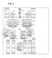
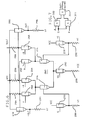
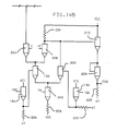
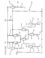
- Fig. 1 depicts a basic unwired cell 10, having eleven transistors T1 - T11, and nine resistors R1 - R9 arranged to permit metallization wiring connections to form one of the aforementioned logic primitives.
- the collectors, emitters and bases of the transistors are identified by the letters C, E, and B, respectively. Formation of these resistive and transistor elements on a masterslice substrate is according to conventional and well known masterslice integrated circuit techniques. For example, the techniques described in U.S. -A- 4,249,193, may be employed to form these devices in the pattern shown.
- Resistor values are as follows: R1 and R2 Top: 552 ohm Bottom: 277 ohm R3, R4, R5 and R6 Top: 1421 ohm Bottom: 2840 ohm R7 Top: 954 ohm Bottom: 1908 ohm RT Top: 5520 ohm Bottom: 2770 ohm
- a significant portion 12 of cell 10 contains no devices. This portion 12 is reserved for first level metallization global wiring. It is desirable to reserve such portion of a cell embodying the present invention for first level metallization global wiring because DCCS uses differential signal lines -- doubling the number of signal lines as compared with ECL current switch masterslice. The amount of additional space in a cell reserved for first level metallization global wiring is a function of the total number of cells in the chip. As the number of cells increases, so does the amount of global wiring per cell.
- resistors have an intermediate tap point which permits selection among three different resistor values, depending upon whether the wiring connections are to the bottom two, top two or bottom and top tap points. This allows the designer to select a low, medium or high power circuit, depending upon the selected resistor values, with corresponding low, medium or high performance, respectively.
- the multi-function primitive logic block 20 is shown in Fig. 2. Both inputs and the output are DCCS signals and are of the same levels.
- the current, I O of the current source comprising transistor 38 and resistor 54
- the current, I O of the current source flows through transistors 22 and 26 and resistor 44, causing -OUT to be at an up level and +OUT to be at a down level.
- the voltage difference between +OUT and -OUT equals I0R, where I0 equals the current flowing through current source transistor 38 and R equals the value of resistor 44 or resistor 46, which are substantially identical.
- Transistors 30 and 32 are emitter followers used to shift the DCCS input signals to the lower level of the cascode circuit.
- the DCCS two-way exclusive OR circuit is shown in Fig. 4.
- Fig. 4 When +A is positive and +B is negative or when +A is negative and +B is positive, the current flows through R88 and +OUT is positive.
- the +B, -B input signals are translated to the lower DCCS level by the emitter follower transistors 74 and 76.
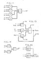
- Fig. 5 shows the logic function for the two-way exclusive OR circuit of Fig. 4.
- the inverse of the exclusive OR function can easily be obtained by swapping the signal pairs of either of the two input variables or by swapping the output signal pairs.
- Multi-way selectors can be implemented using a DCCS circuit similar to the multi-port latch circuit.
- a two-way selector is shown in Fig. 6, with its logic function in Fig. 7.
- the circuit of Fig. 6 is identical to the exclusive OR circuit 60 shown in Fig. 4, except that input variables A and B are different, whereas they are the same in Fig. 4.
- transistors 262, 264, 266, 268, 270, 272, 274, 276, 278, 280, and 282, and resistors 284, 286, 288, 290, 292, 294, 296, and 298, correspond to transistors 66, 68, 70, 72, 74, 76, 62, 64, 78, 80, and 82, and resistors 88, 90, 92, 84, 86, 94, 96, and 98, respectively.
- the two-way selector is possibly the most powerful DCCS circuit since it performs a two level logic function with a single stage DCCS logic circuit, and has no restrictions in its inputs. In digital processor applications this circuit is used extensively, along with the multi-function circuit (discussed below) and the exclusive OR circuit 60 (Fig. 4) in implementing random logic functions.
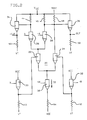
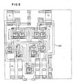
- Fig. 8 is a diagram showing the first level metallization 500 applied to the cell 10 of Fig. 1 required to form the two-way selector depicted in Fig. 6. Note that a single second level wire 50, is required to complete the circuit.
- Fig. 9 shows additional second level metallization 510 required for power connection. It will be understood that additional metallization is required for interconnection of the cell shown in Fig. 9 with other cells on a chip.
- FIG. 10 An example of a four-way selector is shown in Fig. 10. Additional transistor triads 312, 314, 316, and 318, 320, 322, which provide the additional inputs over the two way selector circuit 260 of Fig. 10 can be seen.
- the current from a single current source transistor 324) is steered through one of four transistors (transistors 328, 330, 316, 322) depending on which of their gates is positive (one and only one gate signal must be positive).
- the output is then determined by the data input corresponding to the positive gate signal.
- This circuit has many applications in the data flow areas and requires only one current source. The number of inputs is only limited by leakage and delay effects and can be quite large.
- FIG. 11 A logic model for the four way select circuit 310 of Fig. 10 is shown in Fig. 11.
- the OUT signal equals A(SA) + B(SB) + C(SC) + D(SD).
- a DCCS L1 latch is shown in Fig. 12.
- clock line Cg1 When clock line Cg1 is "on" (positive) the current, I0, flows through transistor 102 and then through transistor 110 or 112 depending on whether +D is positive or negative.
- the value of the data inputs (+D, -D) determine the value of the data outputs (+L1, -L1).
- clock Cg1 turns “off” (-) and HOLD turns “on” the current begins to flow through transistor 104 and through either transistor 114 or 116 depending on whether +L is positive or negative.
- the state of the outputs data (+L, -L) remains unchanged and the input data is stored in the latch.
- the clock "off” the data input (+D, -D) cannot change the state of the latch.
- the clock input to the latch is always a lower level DCCS signal, so an input emitter follower is not required to shift the level of the DCCS signal.
- the latch contains fewer components than a conventional ECL latch, requires only one current source, and has only one stage of delay.
- a transistor pair 108, 122, 124 is included to provide a latch scan function useful in chip testing.
- Fig. 13 illustrates the logic function of the latch of Fig. 12.
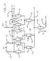
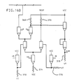
- Fig. 14 is a schematic diagram of an L1 clock driver, for example for the 2-port L1 latch of Fig. 12.
- the L1 clock driver outputs will be orthogonal which is required for the L1 latch.
- Fig. 15 is a logic diagram for the circuit of Fig. 14. As shown by the diagram of Fig. 15, the L1 clock driver provides a CA, or HOLD, signal, a buffered A output, A0, a Cg1 and a Cg2 signal. Signals Cg1 and Cg2 are clock signals having the leading and trailing edges shaped by clock C, and having a level controlled by input signals g1 and g2.
- Fig. 15 The logic elements depicted in Fig. 15 can be related to the circuit elements depicted in Fig. 14.
- AND gate 246 (Fig. 15) is implemented by way of transistors 194, 196, 198, 200, 202, 204, and 206 (Fig. 14).
- Transistor 208 is a voltage translator to the lower level voltage for output signals Cg2.
- AND gate 244 (Fig. 15) is implemented by way of transistors 176, 178, 180, 182, 184, 186, 188, 190 and 192 (Fig. 14).
- AND gate 240 (Fig. 15) is implemented by way of transistors 162, 164 and 166 (Fig. 14). Another voltage translator is provided by way of transistor 174.
- Input voltage translators are provided by way of transistors 176, 188, 194 and 196.
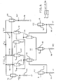
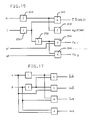
- a gate driver for a four way selector gate driver is shown in Fig. 16. Its structure and operation is similar to the clock driver 160 (Fig. 14), except that all four combinations of the input signals A and B are allowed.
- an N-way gate driver requires N-1 internal current sources plus N emitter followers.
- N-port gate drivers where N is greater than 4, multi-level logic decode is required.
- a logic model for driver 350 is shown in Fig. 17.
- a two-input gated Buss driver is shown. Each driver has a single current source 402, 404 and 406, 408, and can be dotted to an internal DCS buss with load resistors 410 and 412.
- the DCS buss can, of course, drive other DCS circuits.
- exactly one of the n gates must by "on” (plus g1 positive and -g1 negative).
- the circuit designer must be sure that the logic generating these n gates be so designed that for all possible input combinations, one and only one gate is "on”. It is recommended that this be accomplished by designing either logic or physical macros using standard DCS logic circuits.
- the data input signals are standard high-level DCS signals, while the gate inputs are low-level DCS signals and can also be obtained from a high level signal by the emitter followers.
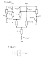
- An Off Chip Receiver Circuit shown in Fig. 20, converts ECL logic level signals to DCCS level signals. In addition, it can be used to perform an OR function between an external, ECL signal and an internal, DCCS signal. Its logic diagram is shown in Fig. 21. The external input signal is B, while the internal input signal is A.
- Fig. 22 is a circuit diagram and Fig. 23 is a logic diagram for that circuit, of one such composite circuit. It illustrates the AND dotting of two of the multi-function two-input circuits shown in Fig. 2.
- the two circuits 520, 522 are AND dotted at their plus outputs, and OR dotted at their negative outputs, as shown.
- Other dot combinations may be made according to well-known techniques.
- a test port is shown.
- This port provides a means for applying a bias to a selected one of the output signal lines. This permits the bias voltage to one side of the output circuit to be varied slightly about a nominal value, to expose marginally valid outputs caused by defective components. During normal operation, this port is simply tied to V CC . This is a highly cost effective test implementation, requiring only one additional resistor. It also has a minimal impact on performance. Other test schemes may be employed, for example to maximise the reliability of the test.
Landscapes
- Physics & Mathematics (AREA)
- Engineering & Computer Science (AREA)
- Computer Hardware Design (AREA)
- Computing Systems (AREA)
- General Engineering & Computer Science (AREA)
- Mathematical Physics (AREA)
- Logic Circuits (AREA)
- Internal Circuitry In Semiconductor Integrated Circuit Devices (AREA)
- Design And Manufacture Of Integrated Circuits (AREA)
Applications Claiming Priority (2)
| Application Number | Priority Date | Filing Date | Title |
|---|---|---|---|
| US06/893,061 US4760289A (en) | 1986-08-04 | 1986-08-04 | Two-level differential cascode current switch masterslice |
| US893061 | 1986-08-04 |
Publications (2)
| Publication Number | Publication Date |
|---|---|
| EP0255589A2 true EP0255589A2 (de) | 1988-02-10 |
| EP0255589A3 EP0255589A3 (de) | 1990-08-29 |
Family
ID=25400971
Family Applications (1)
| Application Number | Title | Priority Date | Filing Date |
|---|---|---|---|
| EP87108641A Ceased EP0255589A3 (de) | 1986-08-04 | 1987-06-16 | Verdrahtbare Schaltungszelle für eine VLSI-Schaltung |
Country Status (3)
| Country | Link |
|---|---|
| US (1) | US4760289A (de) |
| EP (1) | EP0255589A3 (de) |
| JP (1) | JPS6338242A (de) |
Cited By (1)
| Publication number | Priority date | Publication date | Assignee | Title |
|---|---|---|---|---|
| EP0590811A1 (de) * | 1992-10-02 | 1994-04-06 | International Business Machines Corporation | Emitterfolger-Ausgangsstufe mit kapazitiver Kreuzkopplung für Differential-Stromschalterlogik |
Families Citing this family (17)
| Publication number | Priority date | Publication date | Assignee | Title |
|---|---|---|---|---|
| JPH079978B2 (ja) * | 1987-02-24 | 1995-02-01 | 富士通株式会社 | マスタスライス型半導体集積回路 |
| JPS6424443A (en) * | 1987-07-21 | 1989-01-26 | Nec Corp | Gate array |
| JPS6467940A (en) * | 1987-09-08 | 1989-03-14 | Mitsubishi Electric Corp | Semiconductor integrated circuit |
| US4933576A (en) * | 1988-05-13 | 1990-06-12 | Fujitsu Limited | Gate array device having macro cells for forming master and slave cells of master-slave flip-flop circuit |
| US4980579A (en) * | 1988-08-29 | 1990-12-25 | Motorola, Inc. | ECL gate having dummy load for substantially reducing skew |
| EP0410063B1 (de) * | 1989-07-26 | 1996-03-20 | International Business Machines Corporation | Familie logischer Schaltkreise, bestehend aus einem kaskodierten Differentialstromschalter mit Eingangsdioden |
| JPH03109767A (ja) * | 1989-09-25 | 1991-05-09 | Nec Corp | 半導体集積回路装置 |
| US5124591A (en) * | 1990-09-04 | 1992-06-23 | International Business Machines Corporation | Low power push pull driver |
| EP0493989A1 (de) * | 1990-12-31 | 1992-07-08 | International Business Machines Corporation | Masterslice-Chip-Zelle ausgestattet mit einer Vielzahl von Typen logischer Elemente |
| US5166547A (en) * | 1991-06-05 | 1992-11-24 | International Business Machines Corporation | Programmable DCVS logic circuits |
| US5272397A (en) * | 1992-03-27 | 1993-12-21 | International Business Machines Corp. | Basic DCVS circuits with dual function load circuits |
| US5250860A (en) * | 1992-06-25 | 1993-10-05 | International Business Machines Corporation | Three-level cascode differential current switch |
| US5293083A (en) * | 1992-06-30 | 1994-03-08 | International Business Machines Corporation | Fast limited swing push-pull driver |
| US5852367A (en) * | 1992-09-01 | 1998-12-22 | International Business Machines Corporation | Speed enhanced level shifting circuit utilizing diode capacitance |
| US5396182A (en) * | 1992-10-02 | 1995-03-07 | International Business Machines Corporation | Low signal margin detect circuit |
| US6215330B1 (en) | 1999-06-11 | 2001-04-10 | Trw Inc. | Differential diode transistor logic (DDTL) circuit enhancements |
| US6294940B1 (en) | 2000-06-21 | 2001-09-25 | Infineon Technologies North America Corp. | Symmetric clock receiver for differential input signals |
Family Cites Families (11)
| Publication number | Priority date | Publication date | Assignee | Title |
|---|---|---|---|---|
| US3999214A (en) * | 1974-06-26 | 1976-12-21 | Ibm Corporation | Wireable planar integrated circuit chip structure |
| US4249193A (en) * | 1978-05-25 | 1981-02-03 | International Business Machines Corporation | LSI Semiconductor device and fabrication thereof |
| JPS55163859A (en) * | 1979-06-07 | 1980-12-20 | Fujitsu Ltd | Manufacture of semiconductor device |
| US4354266A (en) * | 1979-10-31 | 1982-10-12 | Gte Laboratories Incorporated | Multiplexor with decoding |
| US4408134A (en) * | 1981-01-19 | 1983-10-04 | Advanced Micro Devices, Inc. | Unitary exclusive or-and logic circuit |
| US4513283A (en) * | 1982-11-30 | 1985-04-23 | International Business Machines Corporation | Latch circuits with differential cascode current switch logic |
| US4585957A (en) * | 1983-04-25 | 1986-04-29 | Motorola Inc. | Diode load emitter coupled logic circuits |
| US4615010A (en) * | 1983-06-27 | 1986-09-30 | International Business Machines Corporation | Field effect transistor (FET) cascode current switch (FCCS) |
| GB8324710D0 (en) * | 1983-09-15 | 1983-10-19 | Ferranti Plc | Bipolar transistor logic circuits |
| US4670673A (en) * | 1985-02-19 | 1987-06-02 | Advanced Micro Devices, Inc. | Multilevel differential ECL/CML gate circuit |
| US4686392A (en) * | 1985-10-30 | 1987-08-11 | International Business Machines Corporation | Multi-functional differential cascode voltage switch logic |
-
1986
- 1986-08-04 US US06/893,061 patent/US4760289A/en not_active Expired - Lifetime
-
1987
- 1987-06-16 EP EP87108641A patent/EP0255589A3/de not_active Ceased
- 1987-06-29 JP JP62159943A patent/JPS6338242A/ja active Pending
Cited By (2)
| Publication number | Priority date | Publication date | Assignee | Title |
|---|---|---|---|---|
| EP0590811A1 (de) * | 1992-10-02 | 1994-04-06 | International Business Machines Corporation | Emitterfolger-Ausgangsstufe mit kapazitiver Kreuzkopplung für Differential-Stromschalterlogik |
| US5389832A (en) * | 1992-10-02 | 1995-02-14 | International Business Machines Corporation | Capacitively cross-coupled DCS emitter-follower output stage |
Also Published As
| Publication number | Publication date |
|---|---|
| US4760289A (en) | 1988-07-26 |
| JPS6338242A (ja) | 1988-02-18 |
| EP0255589A3 (de) | 1990-08-29 |
Similar Documents
| Publication | Publication Date | Title |
|---|---|---|
| US4760289A (en) | Two-level differential cascode current switch masterslice | |
| US4527079A (en) | Integrated circuit device accepting inputs and providing outputs at the levels of different logic families | |
| US4918440A (en) | Programmable logic cell and array | |
| US6351152B1 (en) | Look-up table using multi-level decode | |
| US6195788B1 (en) | Mapping heterogeneous logic elements in a programmable logic device | |
| US5038192A (en) | Gate array cell having FETs of different and optimized sizes | |
| US5089973A (en) | Programmable logic cell and array | |
| CA1271234A (en) | Field-programmable logic device with programmable foldback to control number of logic levels | |
| EP0180776B1 (de) | "Chip-on-chip" Halbleitergerät | |
| US5952846A (en) | Method for reducing switching noise in a programmable logic device | |
| EP0068374A2 (de) | Programmierbare logische Anordnung | |
| KR100334001B1 (ko) | 반도체 집적회로의 설계방법 및 자동설계장치 | |
| US4378595A (en) | Synchronous multivalued latch | |
| US6294925B1 (en) | Programmable logic device | |
| US4593205A (en) | Macrocell array having an on-chip clock generator | |
| EP0216756B1 (de) | Integrierte schaltungsvorrichtung, die eingangssignale annimmt und ausgangssignale erzeugt auf den höhen verschiedener logischer scharen | |
| KR100304844B1 (ko) | 반도체집적회로장치 | |
| US5491431A (en) | Logic module core cell for gate arrays | |
| US4441168A (en) | Storage logic/array (SLA) circuit | |
| JP2607538B2 (ja) | 加算回路 | |
| JP3198999B2 (ja) | スキャンパス回路のクロックツリー形成方法 | |
| US4866303A (en) | ECL gate array with collector resistance compensation for distance from power supply pad | |
| US4631425A (en) | Logic gate circuit having P- and N- channel transistors coupled in parallel | |
| US6208166B1 (en) | Circuit and method for implementing combinatorial logic functions | |
| US6646465B2 (en) | Programmable logic device including bi-directional shift register |
Legal Events
| Date | Code | Title | Description |
|---|---|---|---|
| PUAI | Public reference made under article 153(3) epc to a published international application that has entered the european phase |
Free format text: ORIGINAL CODE: 0009012 |
|
| AK | Designated contracting states |
Kind code of ref document: A2 Designated state(s): DE FR GB |
|
| 17P | Request for examination filed |
Effective date: 19880616 |
|
| PUAL | Search report despatched |
Free format text: ORIGINAL CODE: 0009013 |
|
| RHK1 | Main classification (correction) |
Ipc: H03K 19/173 |
|
| AK | Designated contracting states |
Kind code of ref document: A3 Designated state(s): DE FR GB |
|
| 17Q | First examination report despatched |
Effective date: 19920120 |
|
| STAA | Information on the status of an ep patent application or granted ep patent |
Free format text: STATUS: THE APPLICATION HAS BEEN REFUSED |
|
| 18R | Application refused |
Effective date: 19921231 |
|
| RIN1 | Information on inventor provided before grant (corrected) |
Inventor name: RIZZOLO, RICHARD FRANK Inventor name: BELLO, STEPHEN EDWARD Inventor name: EICHELBERGER, EDWARD B. Inventor name: BERGENN, ROLF O. Inventor name: LUDWIG, JOHN ALAN Inventor name: CHU, WILLIAM MAN-SIEW |