EP0248722A2 - Carte à circuit intégré et son connecteur - Google Patents
Carte à circuit intégré et son connecteur Download PDFInfo
- Publication number
- EP0248722A2 EP0248722A2 EP87401223A EP87401223A EP0248722A2 EP 0248722 A2 EP0248722 A2 EP 0248722A2 EP 87401223 A EP87401223 A EP 87401223A EP 87401223 A EP87401223 A EP 87401223A EP 0248722 A2 EP0248722 A2 EP 0248722A2
- Authority
- EP
- European Patent Office
- Prior art keywords
- card
- shutter
- base
- guide
- springs
- Prior art date
- Legal status (The legal status is an assumption and is not a legal conclusion. Google has not performed a legal analysis and makes no representation as to the accuracy of the status listed.)
- Ceased
Links
- 239000004020 conductor Substances 0.000 claims description 3
- 229910000831 Steel Inorganic materials 0.000 claims 1
- 239000010959 steel Substances 0.000 claims 1
- 239000000463 material Substances 0.000 description 8
- 238000003780 insertion Methods 0.000 description 6
- 230000037431 insertion Effects 0.000 description 6
- 239000011248 coating agent Substances 0.000 description 5
- 238000000576 coating method Methods 0.000 description 5
- -1 polyethylene Polymers 0.000 description 5
- 238000003466 welding Methods 0.000 description 4
- 239000004952 Polyamide Substances 0.000 description 3
- 230000006870 function Effects 0.000 description 3
- 239000002184 metal Substances 0.000 description 3
- 229910052751 metal Inorganic materials 0.000 description 3
- 230000004048 modification Effects 0.000 description 3
- 238000012986 modification Methods 0.000 description 3
- 229920002647 polyamide Polymers 0.000 description 3
- 229920000728 polyester Polymers 0.000 description 3
- 239000004698 Polyethylene Substances 0.000 description 2
- 239000004721 Polyphenylene oxide Substances 0.000 description 2
- 239000004734 Polyphenylene sulfide Substances 0.000 description 2
- 239000004743 Polypropylene Substances 0.000 description 2
- 229910000639 Spring steel Inorganic materials 0.000 description 2
- 230000009471 action Effects 0.000 description 2
- 230000006835 compression Effects 0.000 description 2
- 238000007906 compression Methods 0.000 description 2
- 229920001577 copolymer Polymers 0.000 description 2
- 239000000428 dust Substances 0.000 description 2
- 230000000694 effects Effects 0.000 description 2
- 238000000034 method Methods 0.000 description 2
- 239000004033 plastic Substances 0.000 description 2
- 229920003023 plastic Polymers 0.000 description 2
- 229920000573 polyethylene Polymers 0.000 description 2
- 229920006380 polyphenylene oxide Polymers 0.000 description 2
- 229920000069 polyphenylene sulfide Polymers 0.000 description 2
- 229920001155 polypropylene Polymers 0.000 description 2
- 239000004800 polyvinyl chloride Substances 0.000 description 2
- 229920000915 polyvinyl chloride Polymers 0.000 description 2
- 229920005989 resin Polymers 0.000 description 2
- 239000011347 resin Substances 0.000 description 2
- 239000010935 stainless steel Substances 0.000 description 2
- 229910001220 stainless steel Inorganic materials 0.000 description 2
- 229920003002 synthetic resin Polymers 0.000 description 2
- 239000000057 synthetic resin Substances 0.000 description 2
- RYGMFSIKBFXOCR-UHFFFAOYSA-N Copper Chemical compound [Cu] RYGMFSIKBFXOCR-UHFFFAOYSA-N 0.000 description 1
- 229910000881 Cu alloy Inorganic materials 0.000 description 1
- YCKRFDGAMUMZLT-UHFFFAOYSA-N Fluorine atom Chemical compound [F] YCKRFDGAMUMZLT-UHFFFAOYSA-N 0.000 description 1
- 239000004793 Polystyrene Substances 0.000 description 1
- 238000005452 bending Methods 0.000 description 1
- 238000011109 contamination Methods 0.000 description 1
- 229910052802 copper Inorganic materials 0.000 description 1
- 239000010949 copper Substances 0.000 description 1
- 229920003020 cross-linked polyethylene Polymers 0.000 description 1
- 239000004703 cross-linked polyethylene Substances 0.000 description 1
- 230000005611 electricity Effects 0.000 description 1
- 239000011737 fluorine Substances 0.000 description 1
- 229910052731 fluorine Inorganic materials 0.000 description 1
- 230000006872 improvement Effects 0.000 description 1
- 230000009191 jumping Effects 0.000 description 1
- 230000001050 lubricating effect Effects 0.000 description 1
- 229920002492 poly(sulfone) Polymers 0.000 description 1
- 229920000515 polycarbonate Polymers 0.000 description 1
- 239000004417 polycarbonate Substances 0.000 description 1
- 229920002223 polystyrene Polymers 0.000 description 1
- 229920001343 polytetrafluoroethylene Polymers 0.000 description 1
- 229940058401 polytetrafluoroethylene Drugs 0.000 description 1
- 239000004810 polytetrafluoroethylene Substances 0.000 description 1
- 238000003825 pressing Methods 0.000 description 1
- 230000002265 prevention Effects 0.000 description 1
- 238000004080 punching Methods 0.000 description 1
- 230000004044 response Effects 0.000 description 1
- 230000003068 static effect Effects 0.000 description 1
- 238000004804 winding Methods 0.000 description 1
Images


Classifications
-
- H—ELECTRICITY
- H05—ELECTRIC TECHNIQUES NOT OTHERWISE PROVIDED FOR
- H05K—PRINTED CIRCUITS; CASINGS OR CONSTRUCTIONAL DETAILS OF ELECTRIC APPARATUS; MANUFACTURE OF ASSEMBLAGES OF ELECTRICAL COMPONENTS
- H05K5/00—Casings, cabinets or drawers for electric apparatus
- H05K5/02—Details
- H05K5/0256—Details of interchangeable modules or receptacles therefor, e.g. cartridge mechanisms
- H05K5/026—Details of interchangeable modules or receptacles therefor, e.g. cartridge mechanisms having standardized interfaces
-
- H—ELECTRICITY
- H01—ELECTRIC ELEMENTS
- H01R—ELECTRICALLY-CONDUCTIVE CONNECTIONS; STRUCTURAL ASSOCIATIONS OF A PLURALITY OF MUTUALLY-INSULATED ELECTRICAL CONNECTING ELEMENTS; COUPLING DEVICES; CURRENT COLLECTORS
- H01R13/00—Details of coupling devices of the kinds covered by groups H01R12/70 or H01R24/00 - H01R33/00
- H01R13/44—Means for preventing access to live contacts
- H01R13/447—Shutter or cover plate
- H01R13/453—Shutter or cover plate opened by engagement of counterpart
- H01R13/4534—Laterally sliding shutter
Definitions
- This invention relates to an IC card for use in electronic computers and other devices of this kind, particularly a shuttered card-edge type IC card and a connector for connecting the card.
- An IC card has been used for supplying informations to be inputted into or writing informations to be outputted from electronic computers, particularly console units thereof or small electronic computers into which the IC card is inserted.
- electronic computers particularly console units thereof or small electronic computers into which the IC card is inserted.
- memorized informations being broken down if a user's hand touches a connecting terminal portion of the card.
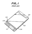
- an IC card as shown in Fig. 1 has been widely used.
- This IC card has a memory portion coated with a coating 112 of a synthetic resin or the like except a connecting terminal portion 111.
- the IC card is provided with a movable shutter 113 between the connecting terminal portion 111 and the coating 112 for covering the terminal portion 111.
- IC card shown in Fig. 1 is a typical one of this kind, which has generally 80-90 mm length, 50-60 mm width and 1.5-2.5 mm thickness.
- the shuttered IC card of the prior art as above described is superior in prevention of dust because of the shutter covering the terminal portion except when being used. Moreover, the shutter somewhat serves as an electrostatic shield. However, such a shuttered IC card encountered the following problems to be solved.
- a shuttered card-edge type IC card including a base having springs therein and a circuit board, a shutter and a cover provided in succession on at least one surface of the base
- the base is formed with guide grooves and guide and spring receiving grooves and the springs for closing the shutter are located in the guide and spring receiving grooves
- the shutter is provided with pawls to be fitted in the guide grooves, respectively, for guiding the pawls in the guide grooves
- the shutter is further provided with spring bias plates to be fitted in the guide and spring receiving grooves, respectively, for guiding the spring bias plates in the guide and spring receiving grooves and biasing the spring bias plates by the springs located therein.
- the shutter is closed by compressive reaction force of the springs received in the base of the card, and opened by ridges provided in a connector into which the card is inserted.
- the guide grooves for guiding the pawls for opening the shutter is provided on the opposite side of terminals with respect to the base so that a surface on the side of the terminals is used only for providing terminals.
- the terminals and shutters are provided on both surfaces of the base and the two shutters are connected so as to be operated simultaneously.
- the shutter and the ground of the internal circuit are electrically conductive through the springs for closing the shutter.
- the connector according to the invention comprises an insulating block provided therein with ridges made of a conductive material corresponding in position and dimension to I-shaped grooves formed in the base of the IC card, and the ridges and the ground of an electronic equipment on a side of the connector are electrically connected.
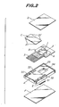
- the IC card according to the invention comprises in outline a base A having springs E provided therein, and a circuit board B, a shutter C and a cover D arranged in succession on at least one surface of the base A .
- Fig. 2 illustrates one embodiment of the IC card according to the invention showing principal parts constituting the card and the relations therebetween.
- the IC card comprises a base, a circuit board provided thereon with for example an integrated circuit, and a shutter C covering a terminal portion 3 of the circuit board B and provided between the circuit board and an upper surface cover D.
- the upper surface cover D covers the circuit board B except its terminal portion 3 and the shutter plate C.
- the IC card further comprises springs E located in spring receiving grooves 33 formed in a bottom surface of the base A and a bottom cover F for the base A .
- the base A is formed in its upper surface with shutter guide grooves 31 (referred to hereinafter “I-shaped grooves”) for guiding pawls 21 of the shutter C and with guide grooves 32 (referred to hereinafter “T-shaped grooves”) for guiding pawls 22 having spring bias plates 23 of the shutter C.
- the T-shaped grooves 32 communicate with the spring receiving grooves 33 formed in the bottom surface of the base A as later explained referring to Figs. 4-7.
- the I-shaped grooves 31, extend halfway in their depth directions over a thickness of the base A without extending through the base A . Although there is no limited condition for the I-shaped grooves 31 other then their depth, they are so designed as to be able to guide the pawls 21 in response to a movement of the shutter C. In general, a depth of 0.5 mm of the grooves suffices to ensure their performance. By determining the depth of the I-shaped grooves in this manner, it is possible to distinguish one surface of the card from the other surface clearly to prevent an erroneous insertion of the card into the connector.
- the base A of the IC card according to the invention is usually provided a frame 35 for settling the circuit board B or the like thereon as shown in Fig. 2.
- the circuit board B to be arranged on the base A often includes an IC chip 1, a battery (not shown), switches (not shown) and others having thicknesses.
- the base A is formed with a recess 34 corresponding to these parts for receiving them.
- Fig. 4 is a perspective view illustrating the base A turned upside down. As shown in Fig. 4, the base A is formed in its bottom surface with the spring receiving grooves 33 capable of receiving the springs E having their free lengths.
- Fig. 5 is a bottom plan view of the base A and Figs. 6a, 6b and 6c are sectional view taken along lines VIa-VIa, VIb-VIb and VIc-VIc in Fig. 5.
- the T-shaped grooves 32 on the upper surface of the base A are shorter than the spring receiving grooves 33 provided in the bottom surface of the base A.
- Fig. 7 illustrates the spring E received in the spring receiving groove 33.
- the bottom cover F is not necessarily a cover covering all over the bottom surface of the base A so long as the cover F is capable of preventing the springs E from jumping out of the spring receiving grooves 33.
- a material, a thickness and the like of the bottom cover F are preferably selected in the same manner as in the shutter C without particular requirements.
- the bottom cover F is preferably made of a stainless steel plate.
- the base A is preferably or the like without any limitation.
- materials for the base A are resins and as polyethylene, polypropylene, polyvinyl chloride, polystyrene, polyamide, polycarbonate, polyester, polyphenylene oxide, polyphenylene sulfide, fluorine plastic material and the like or copolymers of these plastic materials, mixed resins and the like.
- polyethylene, polypropylene, polyvinyl chloride, polyamide, polyester and the like and copolymers thereof are widely used for the base A .
- circuit board B for the IC card according to the invention.
- the circuit board B has been shown in Fig. 2 devoid of the portion corresponding to the I-shaped grooves 31 and T-shaped grooves 32, any configuration of the circuit board B other than that shown may be employed so long as it does not interfere with the movement of the pawls 21 and 22 of the shutter C. This is only a problem in designing the circuit board.
- Fig. 2 exemplarily illustrates the IC provided on the circuit board B, terminals 2 of the IC, terminals 3 of the circuit board B, and a wiring 4 of the circuit.
- a circuit of an IC card may be formed directly on the base A . In this case, the independent circuit board can be dispensed with.
- Fig. 3 is a perspective view illustrating the shutter C shown in Fig. 2 turned upside down.
- the shutter C is provided with pawls 21 and 22 for guiding the movement of the shutter C.
- the pawls 21 and 22 arranged one on forward and rearward sides suffice to perform their functions. If more smooth movement of the shutter is required, two or more pawls 21 and 22 are preferably provided one on the forward and rearward sides.
- the shutter C is moved only when these pawls are subjected to substantially uniform forces but not moved upon being subjected to unequal forces. This effect is preferable in inserting the card into a connector.
- the pawls 22 on the front side in an opening direction of the shutter are provided at their ends with the spring bias plates 23.
- the spring bias plate 23 compress the spring E when the shutter is opened, and is subjected to a compressive reaction force of the spring when the shutter is closed. This compressive reaction force serves to close the shutter.
- the shutter moves on the circuit board B.
- the shutter may be provided on a side of the circuit board with a coating film.
- a material for the coating film is used such as polytetrafluoroethylene, polyamide, polyester, crosslinked polyethylene, polyphenylene oxide, polysulfone, polyphenylene sulfide, and the like.
- a material of the shutter C is not particularly limited. In consideration of thinness, robustness, durability and the like required as a shutter, a metal, particularly a stainless steel is preferable.
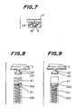
- Figs. 8 and 9 are drawings for explaining how to mount the shutter C after the circuit board B has been provided on the base A.
- Fig. 8 particularly shows the spring E with its free length received in the spring receiving groove 33 formed in the bottom surface of the base A as viewed from the T-shaped groove 32 in the upper surface of the base A.
- a jig 81 in the form of a bar is inserted through the T-shaped groove into the spring E.
- the jig 81 is moved as shown in Fig. 9, so that the spring E is compressed until an end 61 of the spring E arrives at a narrow portion 32b of the groove 32 after it has passed a wide portion 32a of the groove 32.
- the pawls 22 having spring bias plates 23 and the pawls 21 of the shutter C are into the wide portion 32a of the T-shaped grooves 32 and the I-shaped grooves 31, respectively to secure the shutter on the base A.
- the upper cover D is secured to the shutter C.
- a material of the upper cover D is selected in the same manner in the shutter C and the bottom cover F.
- the springs E for closing the shutter C of the IC card according to the invention may be any elongated compression springs.
- coil springs formed by winding spring steel wires about axes and leaf springs formed by zigzag bending band-like spring steel. From the view-points of durability, facility in handling, cost and the like, the coil springs are more preferable.
- Figs. 10a and 10b are drawings for explaining the relation between compressive deformations and functions of the spring E used in the invention.
- the free length is a length of the spring not subjected to any compressive force
- I indicates a pre-compressive deformation which the spring exhibits when the shutter is completely closed
- II indicates a deformation of the spring between the completely closed position and the fully opened position of the shutter.
- Fig. 10b illustrates a relation between the compressive reaction force and the deformation of the spring shown in Fig. 10a.
- the pre-compressive force in the spring at the pre-compressive deformation corresponds to a force acting upon the completely closed shutter. It is understood that the shutter would not open unless any more force effectively acts upon the shutter.
- the grooves 31 for guiding the jaws of the shutter C are provided in the same surface as that on which the terminals are arranged, so that the area in which the terminals are arranged becomes narrower by the area occupied by the grooves 31.
- the memory capacity of the IC card increases to provide for the requirement to have terminals as many as possible.
- FIG. 11a perspectively illustrates another IC card according to the invention.
- Fig. 11b is an exploded perspective view of the IC card shown in Fig. 11a.
- the base A is formed in a bottom surface with the grooves 31 for guiding the pawls 21 of the shutter C.
- the shutter C is provided with the pawls 21 corresponding to the pawls 21 of the base A .
- Fig. 12a illustrates how to secure the shutter C to the board B and base A.
- Fig. 12b shows a configuration of the shutter secured to the board B and base A.
- pawls 21, connecting portions 24 and spring bias plates 23 are formed in L-shaped members. These L-shaped members are passed through the spring receiving grooves 32 from upper surface to bottom surface of the base A so that the shutter C is arranged on the circuit board B provided on the base A .
- the connecting portions 24 and the pawls 21 are bent toward the shutter C into the form of a hair pin shown in two-dot-and-dash lines in Fig. 12a.
- the shutter C is formed into the shape shown in Fig. 2b and the pawls 21 and the connecting portions are received in the grooves 31 in the bottom surface of the base A .
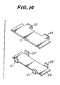
- the shutter C of the IC card according to the invention is only required to have the configuration as shown in Fig. 12b. It may be made by any method other than that above described. For example, it may be that shown in Figs. 13a and 13b. As shown in Fig. 13a, a shutter C provided with spring bias plates 23 is jointed by welding to separately made members consisting of pawls 21, connecting portions 24 and jointing portions 23 ⁇ . In this case, the spring bias plates 23 and the jointing portions 23 ⁇ are connected by welding.
- Fig. 14 illustrates another modification of the shutter C, wherein a shutter C provided with spring bias plates 23 is connected by welding to a separately made member consisting of a connecting portion 24 provided with pawls 21 and jointing portions 23 ⁇ .
- the spring bias plates 23 and the jointing portions 23' are connected by welding.
- the IC cards according to the invention shown in Fig. 2 and Figs. 11a and 11b are provided with the terminals only on one surfaces of the cards, so that they do not sufficiently provide for the requirement to increase the terminals as many as possible. In order to fulfil such a requirement, terminals are provided on both surfaces of the card.
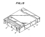
- Fig. 15 is a perspective view illustrating an IC card having terminals on both the surfaces of the card.
- the IC card comprises on a bottom side a circuit board B ⁇ , a shutter C ⁇ (not shown) and a cover D ⁇ successively provided corresponding to those on an upper side.
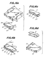
- Figs. 16a-16d illustrate various modifications of the shutter used in the IC card according to the invention. For the reason that the shutters C and C ⁇ provided on the upper and lower surfaces of the base A are simultaneously closed and opened, and for the other reasons, these shutters C and C ⁇ are connected with each other. Any connecting methods may be employed for this purpose, which are shown in Figs. 16a-16d.
- Fig. 16a two shutters C and C ⁇ are connected to form a rectangular cylinder having pawls 21 and 21 ⁇ integrally connected.
- the base A is provided on both sides with grooves 36 for enabling the connecting portions 24 of the shutters C and C ⁇ to move therealong.
- Fig. 16b illustrates two shutters C and C ⁇ connected into a U-shaped member to overlap pawls 21 of the respective shutters C and C ⁇ .
- one edge of the base A is cut off to form grooves 36 for permitting connecting portion 24 of the shutters C and C ⁇ to move therealong.
- Covers D and D' covering the outermost surfaces of the IC card are connected into an integral U-shaped cover.
- Fig. 16c illustrates two separately made upper and lower shutters C and C ⁇ connected by pawls 21 and 21 ⁇ to form a unitary body.
- Fig. 16d shows two shutters C and C ⁇ connected into a U-shaped member. However, either of the overlapped pawls 21 of the shutters C and C ⁇ is dispensed with. In this case, grooves 31 may be provided one in each surface of the base A.
- the guide grooves 31 provided in the base A for the shutters C and C ⁇ are more than two, and shapes and sectional shapes of the guide grooves 31 are made different from each other or they are provided in asymmetry, thereby enabling both surfaces of the IC card to be distinguishable.
- electrostatic trouble can be prevented by electrically connecting the ground of the circuit board B and the shutter C in the card.
- a spring E to be located in a T-shaped groove 32 has one end abutting against a spring bias pawl 23 of a shutter C and the other end 11 which is substantially straight extended and formed with a curved portion.
- the curved portion of the end 11 of the spring is inserted between the base A and the circuit board B so as to be connected with the ground of the circuit board B.
- a contact member 12 having one end abutting against one end of the spring E and the other end 13 adapted to be connected to a ground of the circuit board B.
- FIG. 17b-2 One example of the contact member 12 being secured to the base A is shown in Fig. 17b-2, wherein the contact member is pivotally connected to the base A with the aid of projections integrally formed in the contact member 12 to obtain a stable connection.
- a contact 14 connected to the ground of the circuit board B is planted in the circuit board B and interposed between the T-shaped groove 32 of the base A and the spring E. In this manner, the shutter C and the ground of the circuit board B become conductive through the spring E.
- the circuit board B is provided in the proximity of the T-shaped groove 32 with a suitably sized ground terminal contact 15 which is bent into the T-shaped groove 32 so as to bring the contact 15 into contact with the spring E to obtain an electrical connection between the shutter C and the ground of the circuit board B.
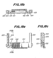
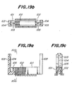
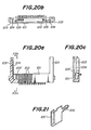
- Figs. 18a-20c Most preferable connectors for the IC cards according to the invention are shown in Figs. 18a-20c. Particularly, the connector shown in Figs. 18a-18c is used for the IC card shown in Fig. 2, the connector shown in Figs. 19a-19c for the IC card having the terminals on both the surfaces shown in Fig. 15 and the connector shown in Figs. 20a-20c for the IC card shown in Figs. 17a-17d providing for the electrostatic trouble.
- each an insulating block 101 has contacts 102 planted therein and is formed with guide legs 103 formed with guide grooves 104.
- the guide legs 103 are not essential for constituting the invention but serve to bring about more effective results.
- the insulating block 101 is formed inside with ridges 105 having positions and dimensions capable of fitting in the I-shaped grooves 31 provided in the base A of the IC card according to the invention to be inserted into the insulating block 101 with the aid of the guidance of the guide legs 103.
- the ridges 105 ⁇ provided in the insulating block 101 shown in Figs. 20a-20c are made of a conductive material. Its one example is shown in Fig. 21.
- the ridge 105 ⁇ shown in Fig. 21 is obtained by stamping or punching a metal plate of copper, copper alloy or the like as used for contacts of connectors into a predetermined shape and further applying to the punched metal plate a suitable working such as pressing.
- the conductive ridges 105 ⁇ may be formed from a conductive synthetic resin.
- Reference numeral 106 denotes a terminal to be connected to a ground of an electronic equipment on the side of the connector.
- the pawls 21 of the shutter C of the IC card are raised by the ridges 105 provided in the insulating block 101 of the connector so as to expose the terminals 3 of the circuit board B of the IC card, thereby bringing the terminals 3 into contact with the contacts 102 of the insulating block 101 of the connector.
- the shutter C of the IC card covers the terminals of the IC card in its completely closed position with the aid of the compressive reaction force of the springs arranged in the base A of the IC card.
- the ridges 105 formed in the insulating block 101 and the I-shaped grooves 31 provided in the base A of the IC card are in a relation as if the ridges 105 and the I-shaped grooves were a "key” and a "lock", so that a wrong insertion of the IC card turned upside down is prevented even in a dark location.
- the pawls 21 of the shutter C of the IC card are raised by the conductive ridges 105 ⁇ to expose the terminals 3 of the circuit board B of the IC card so as to bring the terminals 3 into contact with the contacts 102 planted in the insulating block 101 of the connector. Furthermore, when the IC card is drawn out of the insulating block 101 of the connector, the shutter C of the IC card covers in its fully opened condition the exposed portion of the IC card with the aid of the compressive reaction force of the springs located in the base A of the IC card.
- the IC card and the connector therefor constructed as above described have the following various significant effects which are brought about only by the invention.
Landscapes
- Engineering & Computer Science (AREA)
- Microelectronics & Electronic Packaging (AREA)
- Credit Cards Or The Like (AREA)
- Coupling Device And Connection With Printed Circuit (AREA)
Applications Claiming Priority (10)
| Application Number | Priority Date | Filing Date | Title |
|---|---|---|---|
| JP61128693A JPS62284799A (ja) | 1986-06-03 | 1986-06-03 | Icカ−ド及びそのカ−ドの接続用コネクタ |
| JP128693/86 | 1986-06-03 | ||
| JP61253276A JPS63107596A (ja) | 1986-10-24 | 1986-10-24 | Icカ−ド及びそのicカ−ドの接続用コネクタ |
| JP253276/86 | 1986-10-24 | ||
| JP312422/86 | 1986-12-27 | ||
| JP61315159A JPH0665094B2 (ja) | 1986-12-27 | 1986-12-27 | シヤツタ付icカ−ド用コネクタ |
| JP61312422A JPS63166595A (ja) | 1986-12-27 | 1986-12-27 | シヤツタ−付icカ−ド |
| JP315159/86 | 1986-12-27 | ||
| JP86190/87 | 1987-04-08 | ||
| JP62086190A JPH0780380B2 (ja) | 1987-04-08 | 1987-04-08 | シヤツタ付カ−ドエツジ形icカ−ド |
Publications (2)
| Publication Number | Publication Date |
|---|---|
| EP0248722A2 true EP0248722A2 (fr) | 1987-12-09 |
| EP0248722A3 EP0248722A3 (fr) | 1989-07-12 |
Family
ID=27525212
Family Applications (1)
| Application Number | Title | Priority Date | Filing Date |
|---|---|---|---|
| EP87401223A Ceased EP0248722A3 (fr) | 1986-06-03 | 1987-06-02 | Carte à circuit intégré et son connecteur |
Country Status (3)
| Country | Link |
|---|---|
| US (1) | US4780793A (fr) |
| EP (1) | EP0248722A3 (fr) |
| CA (1) | CA1282155C (fr) |
Cited By (4)
| Publication number | Priority date | Publication date | Assignee | Title |
|---|---|---|---|---|
| EP0328077A3 (en) * | 1988-02-12 | 1990-07-04 | Seiko Epson Corporation | Arrangement for protecting electronic devices against static electricity |
| EP0302530A3 (en) * | 1987-08-07 | 1990-12-19 | Oki Electric Industry Company, Limited | Ic card connecting mechanism |
| EP0453672A1 (fr) * | 1990-04-26 | 1991-10-30 | Mitsubishi Denki Kabushiki Kaisha | Carte à circuits intégrés |
| DE102009028050A1 (de) * | 2009-07-28 | 2011-02-03 | Knorr-Bremse Systeme für Nutzfahrzeuge GmbH | Steckverbindung einer mechatronischen Baugruppe eines Kraftfahrzeuges |
Families Citing this family (38)
| Publication number | Priority date | Publication date | Assignee | Title |
|---|---|---|---|---|
| JP2763290B2 (ja) * | 1987-02-04 | 1998-06-11 | キヤノン株式会社 | 定着ローラ及び定着装置 |
| JPH0164864U (fr) * | 1987-10-21 | 1989-04-26 | ||
| DE3736258A1 (de) * | 1987-10-27 | 1989-05-11 | Mannesmann Kienzle Gmbh | Datenkartenanordnung |
| JPH01134366U (fr) * | 1988-03-07 | 1989-09-13 | ||
| USD322604S (en) | 1988-10-04 | 1991-12-24 | Hosiden Electronics Co., Ltd. | Memory card connector |
| US5289339A (en) * | 1989-06-28 | 1994-02-22 | Kabushiki Kaisha Toshiba | Portable electronic device with memory card unit having symmetrical terminals |
| US5086336A (en) * | 1990-04-27 | 1992-02-04 | Mitsubishi Denki Kabushiki Kaisha | Semiconductor device card |
| DE4028966A1 (de) * | 1990-09-12 | 1992-03-19 | Rudolf Dr Goedecke | Anschluesse an ic - speicherkarten und steckmodule, ueber die analoge oder digitale signale in ein datenverarbeitungsgeraet ein- und ausgegeben werden koennen |
| US5367571A (en) * | 1992-12-02 | 1994-11-22 | Scientific-Atlanta, Inc. | Subscriber terminal with plug in expansion card |
| US5526235A (en) * | 1994-06-23 | 1996-06-11 | Garmin Communication And Navigation | Electronic storage device and receptacle |
| FR2721731B1 (fr) * | 1994-06-24 | 1996-08-09 | Schlumberger Ind Sa | Carte à mémoire. |
| USD364398S (en) | 1994-08-19 | 1995-11-21 | Apple Computer, Inc. | Adapter sleeve for a PCMCIA device |
| US5600539A (en) * | 1994-10-11 | 1997-02-04 | At&T Global Information Solutions Company | Secure interface card extractor/ejector mechanism |
| US5627729A (en) * | 1995-04-03 | 1997-05-06 | Methode Electronics, Inc. | One-piece memory card |
| JP3019280U (ja) * | 1995-05-18 | 1995-12-12 | モレックス インコーポレーテッド | Icカード用ホルダ |
| JPH08337083A (ja) * | 1995-06-13 | 1996-12-24 | Mitsubishi Electric Corp | Icカード |
| JP3173438B2 (ja) * | 1997-06-04 | 2001-06-04 | ソニー株式会社 | メモリカード及び装着装置 |
| JPH11144450A (ja) * | 1997-11-10 | 1999-05-28 | Fujitsu Takamisawa Component Ltd | メモリカード |
| US6704204B1 (en) * | 1998-06-23 | 2004-03-09 | Intel Corporation | IC package with edge connect contacts |
| US6250934B1 (en) | 1998-06-23 | 2001-06-26 | Intel Corporation | IC package with quick connect feature |
| US6282097B1 (en) | 1998-10-28 | 2001-08-28 | Garmin Corporation | Data card having a retractable handle |
| US6215671B1 (en) | 1998-12-10 | 2001-04-10 | Garmin Corporation | Method and apparatus for connecting circuit boards |
| US6250553B1 (en) | 1998-12-30 | 2001-06-26 | Garmin Corporation | Data card having a retractable handle |
| JP3065310B1 (ja) * | 1999-03-19 | 2000-07-17 | 山一電機株式会社 | Icカ―ドの接続機構におけるロックアンドロック解除機構 |
| US6213403B1 (en) | 1999-09-10 | 2001-04-10 | Itt Manufacturing Enterprises, Inc. | IC card with fingerprint sensor |
| US6186809B1 (en) * | 1999-12-09 | 2001-02-13 | Compal Electronics, Inc. | Electronic device with a floating electrical connector unit |
| US7300292B2 (en) * | 2001-07-13 | 2007-11-27 | Hosiden Corporation | Jack type connector with a shutter, and plug type connector |
| US6908342B2 (en) * | 2001-10-02 | 2005-06-21 | Canon Kabushiki Kaisha | Connector, electronic equipment using the connector and information processing unit |
| JP2003110259A (ja) * | 2001-10-02 | 2003-04-11 | Canon Inc | コネクタ、電子機器及び情報処理装置 |
| DE10208168C1 (de) * | 2002-02-26 | 2003-08-14 | Infineon Technologies Ag | Datenträgerkarte |
| DE10216198C1 (de) * | 2002-04-12 | 2003-10-02 | Abb Patent Gmbh | Steckdosensockel mit darin integrierter Berührungsschutzvorrichtung |
| US6848921B2 (en) * | 2003-05-28 | 2005-02-01 | Fci Americas Technology, Inc. | Electrical connector with module ejection system |
| US7908080B2 (en) | 2004-12-31 | 2011-03-15 | Google Inc. | Transportation routing |
| CN102092560A (zh) * | 2011-01-24 | 2011-06-15 | 李超 | 输送机皮带自动纠偏器 |
| US9478892B2 (en) | 2013-08-29 | 2016-10-25 | Hubbell Incorporated | Tamper-resistant assembly with wear-resistant shutters |
| CN107112667A (zh) * | 2014-11-03 | 2017-08-29 | 3M创新有限公司 | 连接器 |
| US10141674B2 (en) | 2016-06-09 | 2018-11-27 | Hubbell Incorporated | Tamper resistant mechanism for electrical wiring devices |
| CN113302804B (zh) | 2018-07-06 | 2023-09-22 | 哈勃股份有限公司 | 一种电配线设备的防误触机构 |
Family Cites Families (6)
| Publication number | Priority date | Publication date | Assignee | Title |
|---|---|---|---|---|
| GB904694A (en) * | 1960-03-30 | 1962-08-29 | Ass Elect Ind | Improvements relating to sliding shutter devices |
| US4149027A (en) * | 1977-05-27 | 1979-04-10 | Atari, Inc. | TV game cartridge and method |
| JPS59162676A (ja) * | 1983-03-08 | 1984-09-13 | Canon Inc | 電子機器 |
| JPS60100829U (ja) * | 1983-12-14 | 1985-07-09 | 第一電子工業株式会社 | メモリカ−ド用コネクタ |
| JPS60160089A (ja) * | 1984-01-30 | 1985-08-21 | Mitsubishi Plastics Ind Ltd | Icメモリ−カ−ド用接続カ−トリツジ |
| JPS6277996A (ja) * | 1985-09-30 | 1987-04-10 | 三菱電機株式会社 | Icカ−ド |
-
1987
- 1987-05-28 US US07/055,133 patent/US4780793A/en not_active Expired - Fee Related
- 1987-06-02 EP EP87401223A patent/EP0248722A3/fr not_active Ceased
- 1987-06-03 CA CA000538775A patent/CA1282155C/fr not_active Expired - Fee Related
Cited By (5)
| Publication number | Priority date | Publication date | Assignee | Title |
|---|---|---|---|---|
| EP0302530A3 (en) * | 1987-08-07 | 1990-12-19 | Oki Electric Industry Company, Limited | Ic card connecting mechanism |
| EP0328077A3 (en) * | 1988-02-12 | 1990-07-04 | Seiko Epson Corporation | Arrangement for protecting electronic devices against static electricity |
| EP0453672A1 (fr) * | 1990-04-26 | 1991-10-30 | Mitsubishi Denki Kabushiki Kaisha | Carte à circuits intégrés |
| DE102009028050A1 (de) * | 2009-07-28 | 2011-02-03 | Knorr-Bremse Systeme für Nutzfahrzeuge GmbH | Steckverbindung einer mechatronischen Baugruppe eines Kraftfahrzeuges |
| DE102009028050B4 (de) * | 2009-07-28 | 2024-06-06 | Knorr-Bremse Systeme für Nutzfahrzeuge GmbH | Steckverbindung einer mechatronischen Baugruppe eines Kraftfahrzeuges |
Also Published As
| Publication number | Publication date |
|---|---|
| US4780793A (en) | 1988-10-25 |
| CA1282155C (fr) | 1991-03-26 |
| EP0248722A3 (fr) | 1989-07-12 |
Similar Documents
| Publication | Publication Date | Title |
|---|---|---|
| US4780793A (en) | IC card and connector therefor | |
| US6699061B2 (en) | Card connector | |
| US4780604A (en) | IC-incorporated memory card | |
| US5790659A (en) | Subscriber identity module (SIM) card holder | |
| US6402529B2 (en) | Card connector | |
| US6004155A (en) | Card connector | |
| EP0195865B1 (fr) | Connexion à dispositif d'insertion pour une carte à circuit intégré ainsi qu'une telle carte | |
| EP1116159B1 (fr) | Connecteur electrique destine a la connexion simultanee de deux cartes memoire electroniques | |
| US6234844B1 (en) | Electronic card connector | |
| US5895286A (en) | Terminal for electrical installations | |
| US7540782B2 (en) | Card connector and method for producing housing assembly | |
| US6607404B1 (en) | Card connector | |
| KR100308355B1 (ko) | 오삽입 방지기구부 ic카드 커넥터 | |
| JPH1074244A (ja) | コンビチップカード用の接触ユニット | |
| JP2006505107A (ja) | 2つのリボン状導体を接続するためのプラグコネクタ及びそれに関連するプラグコネクタシステム | |
| EP1059600B1 (fr) | Ensemble portable de lecture de carte intelligente | |
| US6844107B2 (en) | Battery holder for button-type battery | |
| JP2006505105A (ja) | 可撓性リボンケーブル用クランプコネクタ | |
| US7051931B2 (en) | Chip card reader | |
| US7118420B1 (en) | Dual-slot card connector capable of avoiding erroneous insertion of two cards at once | |
| US6629644B2 (en) | Memory card connector for preventing memory card from short circuit | |
| GB2298743A (en) | A connector for making surface electrical connections to IC cards | |
| CA2229817C (fr) | Bloc de contact fixe par encliquetage | |
| JP2003045574A (ja) | カードアダプタ | |
| CN1144149C (zh) | 与便携式数据媒体交换信息的装置 |
Legal Events
| Date | Code | Title | Description |
|---|---|---|---|
| PUAI | Public reference made under article 153(3) epc to a published international application that has entered the european phase |
Free format text: ORIGINAL CODE: 0009012 |
|
| AK | Designated contracting states |
Kind code of ref document: A2 Designated state(s): DE FR GB |
|
| PUAL | Search report despatched |
Free format text: ORIGINAL CODE: 0009013 |
|
| AK | Designated contracting states |
Kind code of ref document: A3 Designated state(s): DE FR GB |
|
| 17P | Request for examination filed |
Effective date: 19891218 |
|
| 17Q | First examination report despatched |
Effective date: 19920617 |
|
| STAA | Information on the status of an ep patent application or granted ep patent |
Free format text: STATUS: THE APPLICATION HAS BEEN REFUSED |
|
| 18R | Application refused |
Effective date: 19921211 |
|
| RIN1 | Information on inventor provided before grant (corrected) |
Inventor name: OHTSUKI, TOMONARI |