EP0248550A1 - Spannungssteuerungssystem - Google Patents
Spannungssteuerungssystem Download PDFInfo
- Publication number
- EP0248550A1 EP0248550A1 EP87304202A EP87304202A EP0248550A1 EP 0248550 A1 EP0248550 A1 EP 0248550A1 EP 87304202 A EP87304202 A EP 87304202A EP 87304202 A EP87304202 A EP 87304202A EP 0248550 A1 EP0248550 A1 EP 0248550A1
- Authority
- EP
- European Patent Office
- Prior art keywords
- signal
- circuit
- supply
- responsive
- voltage
- Prior art date
- Legal status (The legal status is an assumption and is not a legal conclusion. Google has not performed a legal analysis and makes no representation as to the accuracy of the status listed.)
- Granted
Links
- 101150087426 Gnal gene Proteins 0.000 claims 1
- 230000005669 field effect Effects 0.000 claims 1
- 230000000977 initiatory effect Effects 0.000 claims 1
- 239000003990 capacitor Substances 0.000 description 4
- 238000010586 diagram Methods 0.000 description 1
- 238000004804 winding Methods 0.000 description 1
Images

Classifications
-
- F—MECHANICAL ENGINEERING; LIGHTING; HEATING; WEAPONS; BLASTING
- F02—COMBUSTION ENGINES; HOT-GAS OR COMBUSTION-PRODUCT ENGINE PLANTS
- F02P—IGNITION, OTHER THAN COMPRESSION IGNITION, FOR INTERNAL-COMBUSTION ENGINES; TESTING OF IGNITION TIMING IN COMPRESSION-IGNITION ENGINES
- F02P15/00—Electric spark ignition having characteristics not provided for in, or of interest apart from, groups F02P1/00 - F02P13/00 and combined with layout of ignition circuits
- F02P15/001—Ignition installations adapted to specific engine types
- F02P15/003—Layout of ignition circuits for gas turbine plants
Definitions
- This invention relates to a control system for deriving a substantially constant voltage from an alternating supply of variable frequency and amplitude.
- the invention relates to a system for supplying a substantially constant voltage to a spark igniter arrangement for a gas turbine engine, where this voltage is to be derived from an alternator which is driven by the engine.
- the output of the engine-driven alternator will vary considerably in frequency and amplitude. If the arrangement is to provide an adequate spark discharge at low voltage, such as when the engine is started, the spark discharge at higher engine speeds may damage the igniter.
- a system for deriving a substantially constant output voltage from an alternating supply of variable frequency and amplitude comprising a circuit responsive to a detectable point in each cycle of the supply for generating a control signal whose duration depends on the number of said detectable points which occur in a predetermined time, means responsive to said control signal for interrupting said alternating supply, and an output circuit for deriving said output voltage from the interrupted supply.
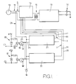
- a generator l0 which is driven by a gas turbine engine (not shown) supplies an alternating voltage on lines ll to a spark voltage output circuit l3 by way of a switching circuit l4 and a transformer l5.
- the circuit l3 supplies a voltage pulse to each of two spark igniters l6.
- the switching circuit l4 is responsive to control signals T on pairs of lines l7, l8 and l9, 20 from respective identical control signal generating circuits 2l, 22.
- the circuits 2l, 22 are responsive to signals on a line 23 from one of the lines ll and also to a signal on a line 24 indicative of a requirement to energise the igniters l6, the signals on line 24 being derived from a +5v supply in a manner to be described.
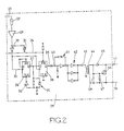
- the circuit 2l includes a Schmidtt trigger circuit 30 and a zener diode 3l to both of which the signal on line 23 is applied by way of a resistor 32 and an amplifier circuit 29.
- the threshold of the trigger circuit 30 is close to 0v so that a positive pulse is provided on a line 33 at a detectable point on each cycle of the supply on lines ll, this point being the negative-going zero crossing point of the alternator output.
- the amplifier circuit 29 ensures that if the supply on line ll becomes erratic in such a manner that the magnitude of a negative-going excursion is small, that excursion will nevertheless be detected and the pulse on line 33 be provided.
- the pulse on line 33 is applied to a clock terminal of D type bistable 34 whose D terminal is maintained at +5v, giving an output signal QA which goes positive in response to the clock pulse on line 33.
- This output signal QA is applied through a timing circuit 35 and inverter 36 to the clear terminal CLR of the bistable 34, the arrangement being such that the output QA on a line 37 persists for 0.6 milliseconds in response to the clock signal CK on line 33.
- the output voltage of the transformer 44 is half-wave rectified by a diode 45 to provide a d.c. voltage across lines l7, l8.
- a depletion-mode FET 46 is connected between the lines l7, l8. Alternate half cycles from the transformer 44 pass through a resistor 47 and a diode 48 and maintain a voltage on the gate of the FET 46 which render it non-conductive. Voltage on the gate of the FET 46 is smoothed by a capacitor 49.
- the circuit l4 includes two enhancement-mode FETs 50, 5l having their sources commonly connected to the line l8 and their gates connected to the line l7.
- Two further enhancement mode FETs 52, 53 have their sources commonly connected to the line 20 and their gates to the line l9.
- the FETs 50, 5l and the FETs 52, 53 respectively are biased to permit current flow to the primary of the transformer l5 ( Figure l).
- the source-gate capacitance of the FETs in the circuit l4 is shorted out, ensuring that these devices have a rapid switch-off response when the signals T on line l7, l9 are removed.
- the source-gate capacitance of these FETs is effective to smooth the half-wave rectified d.c. on the lines l7, l9.
- the secondary winding of the transformer l5 is connected through a known form of rectifier and voltage doubling circuit 60 to an earth rail 6l and to a high voltage rail 62.
- a spark discharge device 63 is connected between the rails 6l, 62.
- Capacitors 64, 65 are connected between the rail 62 and lines 66 and 67 which are in turn connected to the rail 6l through respective identical diode arrangements 68, 69, such that the lines 66, 67 are prevented from becoming negative with respect to the earth rail 6l.
- Identical resistor chains 70, 7l of 3k ohms each are connected in parallel with the respective diode arrangements 68, 69.
- Lines 66, 67 communicate by way of respective chokes 72, 73 whith respective ones of the spark igniters l6 ( Figure l).
- the voltage doubling circuit 60 responds to alternating output from the transformer l5 to increase the voltage on the rail 62 to -3kV, charging the capacitors 64, 65 correspondingly, the lines 66, 67 being at this stage close to earth potential by virtue of the low resistance of the chains 70, 7l.
- the spark discharge device 63 breaks down at -3kV, connecting the rail 62 to earth and bringing the potential on the lines 66, 67 to +3kV which is discharged through respective ones of the igniters l6 ( Figure l). Since the diode arrangements 68, 69 prevent the rails 66, 67 from going negative the spark discharge does not continue after the voltage on these rails has dropped to earth potential.
- identical isolating circuits 80, 8l are responsive to respective identical control signals Cl, C2 from a controlling computer (not shown).
- the circuit 80 includes a light-emitting diode 82 energised from a +5v source only when the signal Cl is low, in which circumstance a photo transistor 83 is switched on and connects the line 24 to earth, maintaining the output QB of the bistable 38 permanently high, whereby the FETs in circuit l4 permanently interrupt current flow.
- the signal Cl is high the transistor 83 is off and the signal on line 24 is +5v, enabling the bistable 34 to respond to clock signals on the line 33. Since the line 24 from circuit 80 is connected to the corresponding line from circuit 8l, it will be apparent that both signals Cl, C2 must be high to permit the igniters l6 to operate.
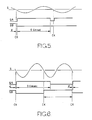
- Figure 5 shows the signals QA, QB from the bistables 34, 38 respectively when the frequency of the alternating supply S is less than l667Hz, that is when the time for one alternating cycle exceeds the 0.6msec output of the signal QA.
- the negative-going cross over of the alternating supply S provides a clock signal CK to bistables 34, 38.
- the output QA goes high for 0.6msec, and because of propagation delay, indicated at d, in bistable 34 the D input of bistable 38 is not high during the initial clock signal CK.
- the output QB thus remains low. The same condition obtains at the subsequent clock signals CK so that QB remains low.
- the oscillator 4l is permanently energised and maintains a signal T on line l7 to keep the FETs 50, 5l switched on, so that alternating supply to the transformer l5 is not interrupted.
- the foregoing also applies to the circuit 22 and the FETs 52, 53.
- Figure 6 shows signals QA, QB when the interval between clock signals CK is just less than 0.6msec, that is with a supply frequency just over l667Hz. Initially QA goes high and QB stays low, as before. At the next succeeding clock signal CK QA is high and QB is thereby set high, and remains high until a clock signal occurs when QA is low. The effect is that when only one clock signal occurs during the time when QA is high the signal QB is high for one cycle of the supply S, which is therefore interrupted for that time.
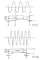
- Figure 7 shows signals QA, QB when two clock signals occur in the 0.6msec high level QA signal, that is when the frequency of supply S is greater than 3333Hz. It will be seen that QB goes high to interrupt the alternating supply for two cycles in every three thereof.
- Figure 8 shows four clock signals occurring in the 0.6msec high level of signal QA, that is when the supply frequency is greater than 6667Hz.
- the supply S is interrupted for four cycles out of every five.
- the arrangement thus reduces the duration of input to the transformer in a stepwise fashion with the increase in supply frequency which results from an increase in alternator speed. Since the rms voltage of the supply S also increases with alternator speed the general effect is that the product of rms voltage and duration of its application to the transformer l5 remains within relatively narrow limits at frequencies over l667Hz.
Landscapes
- Engineering & Computer Science (AREA)
- Chemical & Material Sciences (AREA)
- Combustion & Propulsion (AREA)
- Mechanical Engineering (AREA)
- General Engineering & Computer Science (AREA)
- Ignition Installations For Internal Combustion Engines (AREA)
- Rectifiers (AREA)
- Control Of Electrical Variables (AREA)
- Ac-Ac Conversion (AREA)
- Generation Of Surge Voltage And Current (AREA)
Applications Claiming Priority (2)
| Application Number | Priority Date | Filing Date | Title |
|---|---|---|---|
| GB8613737 | 1986-06-06 | ||
| GB868613737A GB8613737D0 (en) | 1986-06-06 | 1986-06-06 | Voltage control system |
Publications (2)
| Publication Number | Publication Date |
|---|---|
| EP0248550A1 true EP0248550A1 (de) | 1987-12-09 |
| EP0248550B1 EP0248550B1 (de) | 1991-04-10 |
Family
ID=10599024
Family Applications (1)
| Application Number | Title | Priority Date | Filing Date |
|---|---|---|---|
| EP87304202A Expired EP0248550B1 (de) | 1986-06-06 | 1987-05-12 | Spannungssteuerungssystem |
Country Status (6)
| Country | Link |
|---|---|
| US (1) | US4804923A (de) |
| EP (1) | EP0248550B1 (de) |
| JP (1) | JPS6319021A (de) |
| CA (1) | CA1270521A (de) |
| DE (1) | DE3769205D1 (de) |
| GB (1) | GB8613737D0 (de) |
Families Citing this family (4)
| Publication number | Priority date | Publication date | Assignee | Title |
|---|---|---|---|---|
| US4943762A (en) * | 1988-01-27 | 1990-07-24 | Codar Technology, Inc. | Power supply system |
| JPH0810796Y2 (ja) * | 1990-07-02 | 1996-03-29 | 株式会社ツムラ | 生物組織片の試験装置 |
| CN101212149A (zh) * | 2006-12-27 | 2008-07-02 | 鸿富锦精密工业(深圳)有限公司 | 交流电源零点侦测电路 |
| TW200937025A (en) * | 2008-02-29 | 2009-09-01 | Sinpro Electronics Co Ltd | Period determination circuit |
Citations (6)
| Publication number | Priority date | Publication date | Assignee | Title |
|---|---|---|---|---|
| GB1255542A (en) * | 1968-04-24 | 1971-12-01 | Bendix Corp | Pulse generating oscillator circuit |
| US3691404A (en) * | 1971-09-01 | 1972-09-12 | Sperry Rand Corp | Variable duty cycle control circuit |
| US3982175A (en) * | 1973-09-26 | 1976-09-21 | Silec-Semi-Conducteurs | Power regulating device |
| US3991358A (en) * | 1973-11-28 | 1976-11-09 | Stanley Electric Co., Ltd. | Constant voltage device for a magneto alternating current generator |
| US4053733A (en) * | 1974-08-06 | 1977-10-11 | Minolta Camera Kabushiki Kaisha | Temperature control device |
| US4109639A (en) * | 1977-06-13 | 1978-08-29 | Rho Sigma | Solar heating system |
Family Cites Families (3)
| Publication number | Priority date | Publication date | Assignee | Title |
|---|---|---|---|---|
| US3798531A (en) * | 1972-06-05 | 1974-03-19 | Instrumentation Specialties Co | Switching-mode power supply |
| US3979661A (en) * | 1974-12-30 | 1976-09-07 | Dictaphone Corporation | Power supply apparatus having an output voltage within a limited range regardless of input voltage variations and having minimal power dissipation |
| JPS57115022A (en) * | 1981-01-08 | 1982-07-17 | Fuji Xerox Co Ltd | Detecting circuit for zero cross point |
-
1986
- 1986-06-06 GB GB868613737A patent/GB8613737D0/en active Pending
-
1987
- 1987-05-12 EP EP87304202A patent/EP0248550B1/de not_active Expired
- 1987-05-12 DE DE8787304202T patent/DE3769205D1/de not_active Expired - Lifetime
- 1987-05-18 US US07/051,724 patent/US4804923A/en not_active Expired - Lifetime
- 1987-05-26 CA CA000538030A patent/CA1270521A/en not_active Expired
- 1987-06-04 JP JP62139059A patent/JPS6319021A/ja active Pending
Patent Citations (6)
| Publication number | Priority date | Publication date | Assignee | Title |
|---|---|---|---|---|
| GB1255542A (en) * | 1968-04-24 | 1971-12-01 | Bendix Corp | Pulse generating oscillator circuit |
| US3691404A (en) * | 1971-09-01 | 1972-09-12 | Sperry Rand Corp | Variable duty cycle control circuit |
| US3982175A (en) * | 1973-09-26 | 1976-09-21 | Silec-Semi-Conducteurs | Power regulating device |
| US3991358A (en) * | 1973-11-28 | 1976-11-09 | Stanley Electric Co., Ltd. | Constant voltage device for a magneto alternating current generator |
| US4053733A (en) * | 1974-08-06 | 1977-10-11 | Minolta Camera Kabushiki Kaisha | Temperature control device |
| US4109639A (en) * | 1977-06-13 | 1978-08-29 | Rho Sigma | Solar heating system |
Also Published As
| Publication number | Publication date |
|---|---|
| DE3769205D1 (de) | 1991-05-16 |
| GB8613737D0 (en) | 1986-07-09 |
| EP0248550B1 (de) | 1991-04-10 |
| JPS6319021A (ja) | 1988-01-26 |
| CA1270521A (en) | 1990-06-19 |
| US4804923A (en) | 1989-02-14 |
Similar Documents
| Publication | Publication Date | Title |
|---|---|---|
| US5055722A (en) | Gate drive for insulated gate device | |
| US4558404A (en) | Electrostatic precipitators | |
| US4443719A (en) | Voltage isolated gate drive circuit | |
| KR980010988A (ko) | 일렉트로루미네슨스 표시 장치 및 표시 장치의 구동 회로 | |
| US4155113A (en) | Protective circuit for transistorized inverter-rectifier apparatus | |
| US4359650A (en) | High voltage driver amplifier apparatus | |
| US4238723A (en) | Power control system | |
| EP0248550B1 (de) | Spannungssteuerungssystem | |
| US4158224A (en) | Inverter apparatus | |
| GB1227138A (de) | ||
| US6208258B1 (en) | Circuit and method for determining whether AC mains voltage is below or above a predetermined set point | |
| US3448300A (en) | Firing circuit for solid state controllable valves in high di/dt applications | |
| US6777827B1 (en) | Switching arrangement for galvanically insulated control of a load-controlled power switch | |
| US3307073A (en) | Ignition system with series connected transistor and common core inductors to speed switching | |
| US4034240A (en) | Sine-to-square wave converter | |
| CN116937944A (zh) | 功率器件的门极驱动电路、驱动装置及控制方法 | |
| US3333112A (en) | Pulse generator for phase controlled systems | |
| US3492512A (en) | Pulse generating firing and safety circuit for phase controlled silicon controlled rectifiers | |
| US6679237B1 (en) | Ignition drive circuit | |
| US3961235A (en) | Static switch controller synchronized with a passage to zero of the supply voltage | |
| US4153031A (en) | Apparatus for preventing sparks in the ignition system of an engine while the engine is at rest | |
| KR100354726B1 (ko) | 집적형 전력 증폭단을 제어하기 위한 방법 및 장치 | |
| GB2260867A (en) | An A.C. power supply controller for a capacitive load | |
| JPH0974344A (ja) | 絶縁ゲート半導体素子の駆動回路 | |
| JP4085442B2 (ja) | 電源電圧検知形制御装置 |
Legal Events
| Date | Code | Title | Description |
|---|---|---|---|
| PUAI | Public reference made under article 153(3) epc to a published international application that has entered the european phase |
Free format text: ORIGINAL CODE: 0009012 |
|
| AK | Designated contracting states |
Kind code of ref document: A1 Designated state(s): DE FR GB IT SE |
|
| 17P | Request for examination filed |
Effective date: 19880216 |
|
| 17Q | First examination report despatched |
Effective date: 19890505 |
|
| GRAA | (expected) grant |
Free format text: ORIGINAL CODE: 0009210 |
|
| AK | Designated contracting states |
Kind code of ref document: B1 Designated state(s): DE FR GB IT SE |
|
| PG25 | Lapsed in a contracting state [announced via postgrant information from national office to epo] |
Ref country code: SE Effective date: 19910410 |
|
| REF | Corresponds to: |
Ref document number: 3769205 Country of ref document: DE Date of ref document: 19910516 |
|
| PGFP | Annual fee paid to national office [announced via postgrant information from national office to epo] |
Ref country code: SE Payment date: 19910521 Year of fee payment: 5 |
|
| ITF | It: translation for a ep patent filed | ||
| ET | Fr: translation filed | ||
| PLBE | No opposition filed within time limit |
Free format text: ORIGINAL CODE: 0009261 |
|
| STAA | Information on the status of an ep patent application or granted ep patent |
Free format text: STATUS: NO OPPOSITION FILED WITHIN TIME LIMIT |
|
| 26N | No opposition filed | ||
| PGFP | Annual fee paid to national office [announced via postgrant information from national office to epo] |
Ref country code: DE Payment date: 19920529 Year of fee payment: 6 |
|
| PG25 | Lapsed in a contracting state [announced via postgrant information from national office to epo] |
Ref country code: DE Effective date: 19940201 |
|
| PGFP | Annual fee paid to national office [announced via postgrant information from national office to epo] |
Ref country code: FR Payment date: 19980511 Year of fee payment: 12 |
|
| PG25 | Lapsed in a contracting state [announced via postgrant information from national office to epo] |
Ref country code: FR Free format text: LAPSE BECAUSE OF NON-PAYMENT OF DUE FEES Effective date: 20000131 |
|
| REG | Reference to a national code |
Ref country code: FR Ref legal event code: ST |
|
| REG | Reference to a national code |
Ref country code: GB Ref legal event code: IF02 |
|
| REG | Reference to a national code |
Ref country code: GB Ref legal event code: 732E |
|
| PG25 | Lapsed in a contracting state [announced via postgrant information from national office to epo] |
Ref country code: IT Free format text: LAPSE BECAUSE OF NON-PAYMENT OF DUE FEES;WARNING: LAPSES OF ITALIAN PATENTS WITH EFFECTIVE DATE BEFORE 2007 MAY HAVE OCCURRED AT ANY TIME BEFORE 2007. THE CORRECT EFFECTIVE DATE MAY BE DIFFERENT FROM THE ONE RECORDED. Effective date: 20050512 |
|
| PGFP | Annual fee paid to national office [announced via postgrant information from national office to epo] |
Ref country code: GB Payment date: 20060510 Year of fee payment: 20 |
|
| REG | Reference to a national code |
Ref country code: GB Ref legal event code: PE20 |
|
| PG25 | Lapsed in a contracting state [announced via postgrant information from national office to epo] |
Ref country code: GB Free format text: LAPSE BECAUSE OF EXPIRATION OF PROTECTION Effective date: 20070511 |