EP0246784A2 - Joint à déformation réduite pour refroidissement amélioré à l'aide de gaz de plaquette sous vide - Google Patents
Joint à déformation réduite pour refroidissement amélioré à l'aide de gaz de plaquette sous vide Download PDFInfo
- Publication number
- EP0246784A2 EP0246784A2 EP87304092A EP87304092A EP0246784A2 EP 0246784 A2 EP0246784 A2 EP 0246784A2 EP 87304092 A EP87304092 A EP 87304092A EP 87304092 A EP87304092 A EP 87304092A EP 0246784 A2 EP0246784 A2 EP 0246784A2
- Authority
- EP
- European Patent Office
- Prior art keywords
- thermal transfer
- wafer
- ring
- platen surface
- workpiece
- Prior art date
- Legal status (The legal status is an assumption and is not a legal conclusion. Google has not performed a legal analysis and makes no representation as to the accuracy of the status listed.)
- Ceased
Links
Images
Classifications
-
- H—ELECTRICITY
- H10—SEMICONDUCTOR DEVICES; ELECTRIC SOLID-STATE DEVICES NOT OTHERWISE PROVIDED FOR
- H10P—GENERIC PROCESSES OR APPARATUS FOR THE MANUFACTURE OR TREATMENT OF DEVICES COVERED BY CLASS H10
- H10P72/00—Handling or holding of wafers, substrates or devices during manufacture or treatment thereof
- H10P72/04—Apparatus for manufacture or treatment
- H10P72/0431—Apparatus for thermal treatment
-
- H—ELECTRICITY
- H10—SEMICONDUCTOR DEVICES; ELECTRIC SOLID-STATE DEVICES NOT OTHERWISE PROVIDED FOR
- H10P—GENERIC PROCESSES OR APPARATUS FOR THE MANUFACTURE OR TREATMENT OF DEVICES COVERED BY CLASS H10
- H10P72/00—Handling or holding of wafers, substrates or devices during manufacture or treatment thereof
- H10P72/70—Handling or holding of wafers, substrates or devices during manufacture or treatment thereof for supporting or gripping
- H10P72/78—Handling or holding of wafers, substrates or devices during manufacture or treatment thereof for supporting or gripping using vacuum or suction, e.g. Bernoulli chucks
-
- H—ELECTRICITY
- H10—SEMICONDUCTOR DEVICES; ELECTRIC SOLID-STATE DEVICES NOT OTHERWISE PROVIDED FOR
- H10P—GENERIC PROCESSES OR APPARATUS FOR THE MANUFACTURE OR TREATMENT OF DEVICES COVERED BY CLASS H10
- H10P72/00—Handling or holding of wafers, substrates or devices during manufacture or treatment thereof
- H10P72/04—Apparatus for manufacture or treatment
- H10P72/0402—Apparatus for fluid treatment
-
- H—ELECTRICITY
- H10—SEMICONDUCTOR DEVICES; ELECTRIC SOLID-STATE DEVICES NOT OTHERWISE PROVIDED FOR
- H10P—GENERIC PROCESSES OR APPARATUS FOR THE MANUFACTURE OR TREATMENT OF DEVICES COVERED BY CLASS H10
- H10P72/00—Handling or holding of wafers, substrates or devices during manufacture or treatment thereof
- H10P72/70—Handling or holding of wafers, substrates or devices during manufacture or treatment thereof for supporting or gripping
- H10P72/76—Handling or holding of wafers, substrates or devices during manufacture or treatment thereof for supporting or gripping using mechanical means, e.g. clamps or pinches
Definitions
- This invention relates to processing of workpieces in a vacuum chamber and, more particularly, to apparatus for thermal transfer in a system for processing of semiconductor wafers which utilizes gas as a transfer medium.
- a major objective is to achieve a high throughput in terms of wafers processed per unit time.
- One way to achieve high throughput in an ion beam system is to use a relatively high current beam.
- large amounts of heat may be generated in the wafer.
- gas conduction is known to permit thermal coupling between two opposed surfaces and has been applied to semiconductor processing in vacuum.
- gas is introduced into a cavity between a wafer and a support plate (see US-A-4,264,762).
- the achievable thermal transfer with this approach is limited since bowing of the wafer occurs at relatively low gas pressures.
- a semiconductor wafer is clamped at its periphery onto a shaped platen, and gas under pressure is introduced into the microscopic void region between the platen and the wafer.
- the gas pressure approaches that of the preloading, clamping pressure without any appreciable increase in the wafer-to-platen spacing. Since the gas pressure is significantly increased without any increase in the wafer-to-platen gap, the thermal resistance is reduced and solid-to-solid thermal transfer with gas assistance produces optimum results.
- the gas is supplied from a gas source including means for regulating the pressure coupled to the thermal transfer region behind the wafer.
- One way of inhibiting the flow of gas from the thermal transfer region is to position an elastomer O-ring in a groove in the platen surface near the periphery of the semiconductor wafer. When the wafer is clamped against the platen surface, the O-ring is compressed, thereby forming a peripheral seal around the thermal transfer region.
- the clamping ring for clamping the wafer against the platen surface is typically as close to the wafer periphery as practical, so that otherwise usable wafer area is not blocked by the clamping ring.
- the O-ring is located radially inward from the wafer edge and from the clamping ring to avoid overlapping the wafer flat. Thus, when the wafer is clamped in position, the O-ring exerts a force on the wafer which is opposite in direction to the clamping force and radially inward of the clamping force.
- the center portion of the wafer tends to be lifted, and the pressure between the wafer and the platen surface in the thermal transfer region is reduced.
- the rate of thermal transfer between the wafer and the platen surface is substantially reduced.
- the oppositely directed clamping and O-ring forces stress the semiconductor wafer and, in some cases, have overstressed wafers beyond the normally accepted limit of 5.5 megapascals causing water breakage.
- the wafer can stick to prior art O-rings, causing a highly undesirable interruption in processing to free the wafer.
- the depth of ion penetration into the semiconductor material depends in part on the orientation angle between the crystalline lattice of the semiconductor material and the ion beam. For certain angles, an undesirable effect known as channelling results in excessive ion penetration.
- the incident angle of the ion beam varies over the wafer surface, resulting in spatially variable channelling. It is desirable to avoid such spatially variable channelling by maintaining a constant angle of incidence between the wafer and the ion beam.
- the clamping and O-ring forces described above tend to deform the wafer into a dome, thereby exacerbating the channelling problem.
- US-A-4,542,298 discloses a technique for removal of gas escaping from the thermal transfer region before it reaches the high vacuum chamber. An intermediate region around the periphery of the wafer is vacuum pumped to a pressure below that of the gas in the thermal transfer region. This arrangement is disadvantageous in that a seal is required between the peripheral front surface of the wafer and the high vacuum chamber, thereby complicating the construction of the wafer processing station.
- platen means including a platen surface for supporting the workpiece in a processing position with a surface exposed to the vacuum chamber, means for clamping the workpiece to the platen surface, means for introduction of a gas at a prescribed pressure into a thermal transfer region between the workpiece and the platen surface and means for inhibiting flow of gas from the thermal transfer region to the vacuum chamber.
- the gas flow inhibiting means comprises an elastomer ring having an elongated cross-section and a sealing groove in the platen surface near the periphery of the wafer and surrounding the thermal transfer region.
- the groove includes a first groove portion for firmly gripping a fixed edge portion of the ring so that a movable edge portion of the ring extends above the platen surface and contacts the workpiece.
- the elongated cross-section has a long dimension oriented at an acute angle to the platen surface.
- the sealing groove further includes a second groove portion which receives the movable edge portion of the ring by bending deformation thereof when the workpiece is clamped to the platen surface.
- the elongated cross-section of the elastomer ring have a parallelogram shape and taper essentially to a point where the ring contacts the workpiece. It is further preferred that the first groove portion include parallel sidewalls spaced to firmly grip opposite sides of the fixed edge portion of the ring, the sidewalls being oriented at an acute angle to the platen surface.
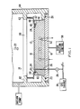
- FIG. 1 An example of apparatus for gas enhanced thermal transfer in accordance with the present invention is shown in simplified form in FIG. 1.
- the apparatus can be utilized in an ion implantation system such as the Model 350D Ion Implantation System manufactured and sold by the Extrion Division of Varian Associates, Inc.
- the target region of the ion implantation system is illustrated in FIG. 1.
- a platen 10 provides support for a semiconductor wafer 12 in a processing position with its front surface exposed to a vacuum chamber 14.
- the platen 10 is typically a metal, such as aluminum, and includes a platen surface 16 which can be domed or curved as described in US-A-4,282,924 and US-A-4,535,835.
- the platen surface 16 can be flat. In FIG. 1 the platen surface 16 is shown as flat, although it will be understood that any curvature is relatively slight.
- the contour of the platen surface 16 is selected to insure intimate contact between the wafer 12 and surface 16.
- the platen 10 can be attached to or can be part of a chamber door 18. An O-ring 20 on the chamber door 18 seals the platen 10 into the vacuum chamber 14.
- an ion beam 22 impinges on the wafer 12 and generates heat therein.
- the wafer 12 is in contact with the curved platen surface 16 in order to remove the heat by conduction.
- the back surface of the wafer 12 and the platen surface 16 actually make contact over less than 5% of the total area due to microscopic surface irregularities. Numerous microscopic voids exist between the actual points of contact. When these voids are evacuated heat conduction is greatly reduced.
- a gas such as air at a prescribed pressure is introduced into the microscopic voids by means of an annular groove 24 in the surface 16 coupled to a passage 26.
- the passage 26 is coupled through a shutoff valve 28 to a gas source 30 at a prescribed pressure which is typically in the range between 100 and 7000 Pascals.
- the gas-filled microscopic voids comprise a thermal transfer region which conducts heat between the wafer 12 and the platen 10. Further details on the technique of gas-enhanced thermal transfer are disclosed in US-A-4,457,359.
- the platen 10 can be provided with passages 32 for circulation of a coolant such as water.
- a spring-loaded clamping ring 40 is attached to a flange 42 which is part of housing 44 which encloses the vacuum chamber 14.
- the clamping ring 40 securely clamps the wafer 12 against the platen surface 16.
- the vacuum chamber 14 and the platen 10 are separated by a vacuum gate valve 46, thereby defining an air lock which permits wafers to be exchanged without venting the vacuum chamber 14.
- the chamber door 18 and the platen 10 are coupled to a position control means 50 which is operative to open the door 18 from the wafer processing position to a wafer transfer position in which wafers are exchanged.
- the control means 50 can, for example, be an air cylinder.
- the apparatus shown in FIG. 1 is provided with a seal between the thermal transfer region and the vacuum chamber 14.
- the seal comprises an elastomer ring 60 located in a groove 62.
- the seal has unique characteristics which permit the thermal transfer region to be effectively sealed from the vacuum chamber 14 without subjecting the wafer 12 to excessive stress.
- the characteristics of the elastomer ring 60 and the groove 62 are described in detail hereinafter.
- the groove 62 extends around the platen surface 16 inside the periphery of the wafer 12 and forms a closed loop which surrounds the thermal transfer region.
- the thermal transfer region is thus defined by the rear surface of the wafer 12, the platen surface 16 and the seal of the present invention.
- the groove 62 is located radially outward of annular groove 24 and is preferably as close to the periphery of the wafer 12 as is practical. When a circular elastomer ring 60 is utilized, it is necessary to position the groove 62 inward of the wafer flat to avoid leakage. When a specially designed elastomer ring having a flat corresponding to the wafer flat is utilized, the groove 62 can be located closer to the wafer periphery.
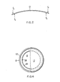
- FIG. 2 there is shown a free-body diagram of the forces exerted on the wafer 12 by the clamping ring 40 and the elastomer ring 60.
- the clamping force F c is outward of the sealing ring force F o .
- Each force is effectively a circular line force tending to depress the outer wafer edge and lift the center portion.
- the line force exerted by prior art circular O-rings is on the order of 1 kg/cm. when a 70 durometer O-ring is compressed by 13.5%. In addition to the stress caused by these forces, lifting of the center portion of the wafer tends to substantially reduce thermal transfer characteristics.
- the forces F o exerted by the elastomer sealing ring are substantially reduced while maintaining a reliable seal against leakage of gas from the thermal transfer region to the vacuum chamber 14.
- gas leakage radially outward between the wafer 12 and the platen surface 16 flows directly to the vacuum chamber 14 causing a degradation in system performance as described hereinabove.
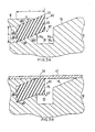
- FIG. 3A A greatly enlarged cross-sectional view of the sealing means of the present invention with no wafer present is shown in FIG. 3A.
- FIG. 3B A similar view is shown in FIG. 3B with a wafer 12 clamped to the platen surface 16.
- the elastomer ring 60 has an elongated cross-section and, in the present example, has a parallelogram shaped cross-section.
- the cross-section shown in FIG. 3A is uniform around the the ring 60.
- the ring 60 is 70 durometer viton, dimension a is 0.127 cm and dimension b is 0.32 cm.
- the groove 62 includes a first groove portion 66 which firmly grips a fixed edge portion 68 of ring 60 so that a movable edge portion 70 of ring 60 extends above the platen surface 16 when no wafer is clamped thereto.
- the ring 60 extends above the platen surface 16 with no wafer present by about 0.058 cm.
- the elongated cross-section of the ring 60 is positioned by the first groove portion 66 so that the long dimension of the elongated cross-section is oriented at acute angle m with respect to the platen surface 16. In the present example the angle m is 22 degrees.
- the first groove portion 66 includes parallel sidewalls 66a, 66b, both oriented at the angle m with respect to the platen surface 16 and a back wall 66c connecting walls 66a and 66b.
- the sidewalls 66a and 66b are spaced to firmly grip the fixed edge portion 68 of the ring 60.
- the movable edge portion 70 of the ring 60 tapers essentially to a point 72, when no wafer is clamped to the platen surface 16.
- the groove 62 further includes a second groove portion 74 which receives the movable edge portion 70 of the ring 60 by bending deformation thereof when a wafer 12 is clamped to the platen surface 16 as shown in FIG. 3B.
- the second groove portion 74 is located adjacent the open end of the first groove portion 66 and includes sidewalls 74a, 74b and a bottom wall 74c.
- the first groove portion 66 and the second groove portion 74 can be fabricated relatively easily on a lathe with appropriate tooIing.
- the sloping portion 78 of platen surface 16 is not a necessary element of the present invention but is typically formed during machining of the first groove portion 66 and does not adversely affect the performance of the apparatus.
- the movable edge portion 70 of the ring 60 is pressed downwardly into the second groove portion 74, while the fixed edge portion 68 remains substantially fixed in position.
- the movable edge portion 70 is depressed by the wafer 12, there is formed a contact area 76 which substantially seals the thermal transfer region and prevents gas leakage into the vacuum chamber 14.
- the depression of the movable edge portion 70 results primarily in a bending or deflection of the cross-section of the elastomer ring 60 and a lesser amount of compression. This provides a substantial reduction in the force applied by the ring 60 to the wafer 12, while maintaining efficient sealing of the thermal transfer region.
- the sealing arrangement of the present invention provides sufficient deflection of the ring 60 upon clamping of a wafer 12 to the platen surface 16 to overcome any irregularities,variations and tolerances and to reliably seal the thermal transfer region.
- the ring 60 is deflected by bending, with very little compression, the force applied to the wafer is minimized and the undesirable effects described hereinabove are alleviated.
- a line loading of about 1275 Pa results. Therefore, wafer stress is greatly reduced in comparison with prior art sealing techniques.
- the cross-section of the elastomer ring 60 is not necessarily a parallelogram in accordance with the present invention.
- An elongated cross-section is required to facilitate bending deformation as described above.
- the first groove portion is not necessarily shaped as shown and described hereinabove. It is required that the first groove portion be shaped to firmly grip one edge portion of the elastomer ring and to position it at an acute angle with respect to the platen surface 16 such that it extends above the platen surface 16 when no wafer is clamped thereto.
- the second groove portion is not necessarily shaped as shown and described hereinabove It is required that the second groove portion provide a space for deflection of the movable edge portion of the ring by bending deformation with minimal compression.
- the chamber door 18 is opened and the wafer 12 is placed on the platen surface 16 and is temporarily retained thereon by a vacuum chuck (not shown) until the door 18 is closed.
- the clamping ring 40 bears against the wafer 12 around its outer periphery and securely clamps the wafer against the platen surface 16.
- the air lock defined by the vacuum gate valve 46 is vacuum pumped and the gate valve 46 is opened.
- the shutoff valve 28 is opened, thereby permitting introduction of gas at the prescribed pressure into the thermal transfer region between the wafer 12 and the platen surface 16. Ion implantation of the wafer 12 now proceeds by scanning of the ion beam 22 over the surface of the wafer 16.
- Heat imparted to the wafer 12 by the ion beam 22 is transferred to the platen 10 by the gas in the thermal transfer region and by direct conduction at the points of physical contact. The heat is then removed from the platen 10 by the coolant circulating through the passages 32.
- the clamping ring 40 clamps the wafer 12 against the platen surface 16, thereby deforming the elastomer ring 60, as shown in FIG. 3B, and restricting the flow of the thermal transfer gas from the thermal transfer region into the vacuum chamber 14.
- the present invention has been described in connection with serial process ion implantation systems, that is, ion implantation systems wherein one wafer at a time is processed by electrostatic scanning. It will be understood that the sealing means of the present invention can be applied to batch type ion implantation systems wherein a plurality of wafers is mounted on a rotating disk for processing. Also, the sealing means is applicable generally to any type of wafer processing in vacuum wherein thermal transfer is required. In addition, the apparatus has been described primarily in terms of wafer cooling. However, certain processes, such as sputtering, require wafer heating. The sealing means of the present invention is equally applicable to processes requiring wafer heating, with the cooled platen replaced by a heating element. Furthermore, the present invention has been described in connection with semiconductor wafers. It will be understood that the apparatus of the present invention can be utilized in connection with any thin workpiece processed in vacuum.
Landscapes
- Container, Conveyance, Adherence, Positioning, Of Wafer (AREA)
- Drying Of Semiconductors (AREA)
Applications Claiming Priority (2)
| Application Number | Priority Date | Filing Date | Title |
|---|---|---|---|
| US06/864,097 US4671204A (en) | 1986-05-16 | 1986-05-16 | Low compliance seal for gas-enhanced wafer cooling in vacuum |
| US864097 | 1997-05-28 |
Publications (2)
| Publication Number | Publication Date |
|---|---|
| EP0246784A2 true EP0246784A2 (fr) | 1987-11-25 |
| EP0246784A3 EP0246784A3 (fr) | 1989-09-06 |
Family
ID=25342526
Family Applications (1)
| Application Number | Title | Priority Date | Filing Date |
|---|---|---|---|
| EP87304092A Ceased EP0246784A3 (fr) | 1986-05-16 | 1987-05-07 | Joint à déformation réduite pour refroidissement amélioré à l'aide de gaz de plaquette sous vide |
Country Status (4)
| Country | Link |
|---|---|
| US (1) | US4671204A (fr) |
| EP (1) | EP0246784A3 (fr) |
| JP (1) | JPH0622214B2 (fr) |
| KR (1) | KR960000949B1 (fr) |
Cited By (2)
| Publication number | Priority date | Publication date | Assignee | Title |
|---|---|---|---|---|
| EP0343502A3 (fr) * | 1988-05-23 | 1991-04-17 | Lam Research Corporation | Méthode et système pour serrer des plaquettes semi-conductrices |
| DE4403553C2 (de) * | 1993-02-06 | 2002-04-18 | Hyundai Electronics Ind | Elektronen-Zyklotron-Resonanz-Apparatur |
Families Citing this family (28)
| Publication number | Priority date | Publication date | Assignee | Title |
|---|---|---|---|---|
| US5228501A (en) * | 1986-12-19 | 1993-07-20 | Applied Materials, Inc. | Physical vapor deposition clamping mechanism and heater/cooler |
| US5871811A (en) * | 1986-12-19 | 1999-02-16 | Applied Materials, Inc. | Method for protecting against deposition on a selected region of a substrate |
| US5484011A (en) * | 1986-12-19 | 1996-01-16 | Applied Materials, Inc. | Method of heating and cooling a wafer during semiconductor processing |
| US4791983A (en) * | 1987-10-13 | 1988-12-20 | Unisys Corporation | Self-aligning liquid-cooling assembly |
| JP2673538B2 (ja) * | 1988-05-02 | 1997-11-05 | 東京エレクトロン株式会社 | エッチング装置及びエッチング方法 |
| US5262029A (en) * | 1988-05-23 | 1993-11-16 | Lam Research | Method and system for clamping semiconductor wafers |
| JPH0682749B2 (ja) * | 1988-06-09 | 1994-10-19 | 日新電機株式会社 | 真空内処理における板状処理物の冷却方法 |
| EP0439000B1 (fr) * | 1990-01-25 | 1994-09-14 | Applied Materials, Inc. | Dispositif de serrage électrostatique et procédé |
| KR940011708B1 (ko) * | 1990-04-09 | 1994-12-23 | 니찌덴 아네루바 가부시끼가이샤 | 기판온도제어기구 |
| EP0452779B1 (fr) | 1990-04-20 | 1996-03-27 | Applied Materials, Inc. | Mécanisme de bridage pour déposition en phase gazeuse par procédé physique |
| US5198753A (en) * | 1990-06-29 | 1993-03-30 | Digital Equipment Corporation | Integrated circuit test fixture and method |
| USH1145H (en) | 1990-09-25 | 1993-03-02 | Sematech, Inc. | Rapid temperature response wafer chuck |
| US5267607A (en) * | 1991-05-28 | 1993-12-07 | Tokyo Electron Limited | Substrate processing apparatus |
| US5131460A (en) * | 1991-10-24 | 1992-07-21 | Applied Materials, Inc. | Reducing particulates during semiconductor fabrication |
| US5352327A (en) * | 1992-07-10 | 1994-10-04 | Harris Corporation | Reduced temperature suppression of volatilization of photoexcited halogen reaction products from surface of silicon wafer |
| US5366002A (en) * | 1993-05-05 | 1994-11-22 | Applied Materials, Inc. | Apparatus and method to ensure heat transfer to and from an entire substrate during semiconductor processing |
| TW277139B (fr) * | 1993-09-16 | 1996-06-01 | Hitachi Seisakusyo Kk | |
| US5368645A (en) * | 1993-09-24 | 1994-11-29 | Specialty Coating Systems Inc. | Vacuum chuck for coating apparatus |
| WO1996008838A1 (fr) * | 1994-09-15 | 1996-03-21 | Materials Research Corporation | Appareil et procede de fixation d'un substrat |
| US5697427A (en) * | 1995-12-22 | 1997-12-16 | Applied Materials, Inc. | Apparatus and method for cooling a substrate |
| JPH10240356A (ja) | 1997-02-21 | 1998-09-11 | Anelva Corp | 基板処理装置の基板温度制御法と基板温度制御性判定法 |
| US6176931B1 (en) | 1999-10-29 | 2001-01-23 | International Business Machines Corporation | Wafer clamp ring for use in an ionized physical vapor deposition apparatus |
| US7993457B1 (en) * | 2007-01-23 | 2011-08-09 | Novellus Systems, Inc. | Deposition sub-chamber with variable flow |
| CN102005395B (zh) * | 2009-08-31 | 2013-03-06 | 日立设备工程股份有限公司 | 真空贴装方法及装置 |
| US9353439B2 (en) | 2013-04-05 | 2016-05-31 | Lam Research Corporation | Cascade design showerhead for transient uniformity |
| US10023959B2 (en) | 2015-05-26 | 2018-07-17 | Lam Research Corporation | Anti-transient showerhead |
| CN108735586B (zh) * | 2017-06-30 | 2021-05-28 | 上海微电子装备(集团)股份有限公司 | 一种抽真空装置及抽真空方法 |
| US11685996B2 (en) * | 2021-03-05 | 2023-06-27 | Sky Tech Inc. | Atomic layer deposition device |
Family Cites Families (6)
| Publication number | Priority date | Publication date | Assignee | Title |
|---|---|---|---|---|
| GB1096171A (en) * | 1964-03-10 | 1967-12-20 | Willi Brandl | Sealing device for containers |
| US4299332A (en) * | 1979-02-22 | 1981-11-10 | Hahn & Clay | Pressure vessel seal |
| US4282924A (en) * | 1979-03-16 | 1981-08-11 | Varian Associates, Inc. | Apparatus for mechanically clamping semiconductor wafer against pliable thermally conductive surface |
| DE3134825A1 (de) * | 1981-09-03 | 1983-03-10 | Inventa Ltd., St. Helier, Jersey, Chanel Islands | Dichtung fuer die zusammenwirkenden verschlussflaechen von druckbehaeltern und deren tueren oder deckel |
| US4457359A (en) * | 1982-05-25 | 1984-07-03 | Varian Associates, Inc. | Apparatus for gas-assisted, solid-to-solid thermal transfer with a semiconductor wafer |
| US4542298A (en) * | 1983-06-09 | 1985-09-17 | Varian Associates, Inc. | Methods and apparatus for gas-assisted thermal transfer with a semiconductor wafer |
-
1986
- 1986-05-16 US US06/864,097 patent/US4671204A/en not_active Expired - Lifetime
-
1987
- 1987-05-06 JP JP62109060A patent/JPH0622214B2/ja not_active Expired - Fee Related
- 1987-05-07 EP EP87304092A patent/EP0246784A3/fr not_active Ceased
- 1987-05-16 KR KR1019870004806A patent/KR960000949B1/ko not_active Expired - Fee Related
Cited By (2)
| Publication number | Priority date | Publication date | Assignee | Title |
|---|---|---|---|---|
| EP0343502A3 (fr) * | 1988-05-23 | 1991-04-17 | Lam Research Corporation | Méthode et système pour serrer des plaquettes semi-conductrices |
| DE4403553C2 (de) * | 1993-02-06 | 2002-04-18 | Hyundai Electronics Ind | Elektronen-Zyklotron-Resonanz-Apparatur |
Also Published As
| Publication number | Publication date |
|---|---|
| JPS62274625A (ja) | 1987-11-28 |
| JPH0622214B2 (ja) | 1994-03-23 |
| KR960000949B1 (ko) | 1996-01-15 |
| EP0246784A3 (fr) | 1989-09-06 |
| KR870011665A (ko) | 1987-12-26 |
| US4671204A (en) | 1987-06-09 |
Similar Documents
| Publication | Publication Date | Title |
|---|---|---|
| US4671204A (en) | Low compliance seal for gas-enhanced wafer cooling in vacuum | |
| US4567938A (en) | Method and apparatus for controlling thermal transfer in a cyclic vacuum processing system | |
| US4535834A (en) | Method and apparatus for controlling thermal transfer in a cyclic vacuum processing system | |
| US4542298A (en) | Methods and apparatus for gas-assisted thermal transfer with a semiconductor wafer | |
| EP0323902B1 (fr) | Dispositif de transfert thermique avec une plaquette semi-conductrice dans le vide | |
| US4527620A (en) | Apparatus for controlling thermal transfer in a cyclic vacuum processing system | |
| US4457359A (en) | Apparatus for gas-assisted, solid-to-solid thermal transfer with a semiconductor wafer | |
| US4508161A (en) | Method for gas-assisted, solid-to-solid thermal transfer with a semiconductor wafer | |
| US6103014A (en) | Chemical vapor deposition chamber | |
| EP0025670B2 (fr) | Procédé et appareil pour transférer de la chaleur à un article traité sous vide, ou pour l'en extraire | |
| EP0452779B1 (fr) | Mécanisme de bridage pour déposition en phase gazeuse par procédé physique | |
| US4938992A (en) | Methods for thermal transfer with a semiconductor | |
| JPH1064888A (ja) | 改良型ガス散布板を用いるエッチング | |
| US4514636A (en) | Ion treatment apparatus | |
| US4997606A (en) | Methods and apparatus for fabricating a high purity thermally-conductive polymer layer | |
| US4717829A (en) | Platen and beam setup flag assembly for ion implanter | |
| JPH0323631B2 (fr) | ||
| US11302557B2 (en) | Electrostatic clamping system and method | |
| JPS61264649A (ja) | 基板冷却装置 | |
| EP1556884A2 (fr) | Structure de support de tranche comprenant un support electrostatique et plaque superieure assurant une protection laterale et une evacuation des gaz | |
| JP2681056B2 (ja) | 真空内の半導体ウエーハの熱移動装置及び方法 | |
| JPS62229948A (ja) | 半導体ウエハ処理装置の冷却装置 | |
| JP2000124295A (ja) | ウェーハホルダ及びこれを備えたイオンミリング装置 | |
| JPS61119037A (ja) | 真空内処理における被処理物の温度制御方法およびその装置 | |
| JPH06172997A (ja) | 基体保持装置 |
Legal Events
| Date | Code | Title | Description |
|---|---|---|---|
| PUAI | Public reference made under article 153(3) epc to a published international application that has entered the european phase |
Free format text: ORIGINAL CODE: 0009012 |
|
| AK | Designated contracting states |
Kind code of ref document: A2 Designated state(s): AT BE CH DE ES FR GB GR IT LI LU NL |
|
| PUAL | Search report despatched |
Free format text: ORIGINAL CODE: 0009013 |
|
| AK | Designated contracting states |
Kind code of ref document: A3 Designated state(s): AT BE CH DE ES FR GB GR IT LI LU NL |
|
| 17P | Request for examination filed |
Effective date: 19900305 |
|
| 17Q | First examination report despatched |
Effective date: 19910926 |
|
| STAA | Information on the status of an ep patent application or granted ep patent |
Free format text: STATUS: THE APPLICATION HAS BEEN REFUSED |
|
| 18R | Application refused |
Effective date: 19921028 |
|
| RIN1 | Information on inventor provided before grant (corrected) |
Inventor name: BALLOU, JON M. |