EP0246539A2 - Silizium-Packungen für Leistungshalbleiteranordnungen - Google Patents
Silizium-Packungen für Leistungshalbleiteranordnungen Download PDFInfo
- Publication number
- EP0246539A2 EP0246539A2 EP87106854A EP87106854A EP0246539A2 EP 0246539 A2 EP0246539 A2 EP 0246539A2 EP 87106854 A EP87106854 A EP 87106854A EP 87106854 A EP87106854 A EP 87106854A EP 0246539 A2 EP0246539 A2 EP 0246539A2
- Authority
- EP
- European Patent Office
- Prior art keywords
- package
- cap
- silicon
- base
- semiconductor wafer
- Prior art date
- Legal status (The legal status is an assumption and is not a legal conclusion. Google has not performed a legal analysis and makes no representation as to the accuracy of the status listed.)
- Granted
Links
Images

Classifications
-
- H10W76/138—
-
- H10W74/137—
-
- H10W76/47—
Definitions
- This invention relates generally to packaging, and more particularly to packages for semiconductor devices.
- Packages for power semiconductor wafers must operate in a variety of different environments and must meet many different requirements. Such packages must provide a housing for the wafer which is secure from external environmental influences which might otherwise damage the wafer. They must provide for electrical connections to the wafer in a manner which is both convenient and does not compromise the protection from the environment. They must provide a cool thermal environment for the wafer and must contact the wafer with materials which permit the wafer to expand and contract with changes in temperature, without causing excessive stresses in the wafer or supportive material. Such packages are also desirably light in weight, compact in size, and easily fabricated using known technologies.
- Prior art packages for power semiconductor wafers typically comprise some combination of metals, plastics and ceramics, each of which compromises one aspect of functionality to emphasize another.
- high thermal conductivity metals such as copper and aluminum can provide excellent heat removal characteristics, but differ substantially from the silicon wafer in thermal expansion. These metals thus cause thermal fatigue and premature failure at the interfaces between the wafer and package.
- Some ceramic materials may be selected to more closely match the thermal expansion of the wafer, but do not provide for easy electrical connection to the wafer.
- Some plastic materials may be easily fabricated into various package configurations, but these plastics may not provide for heat removal or electrical connections.
- metals and ceramics can be used to fabricate packages with selected functional characteristics, each of these materials has its own drawbacks which makes its use in the package to some extent undesirable.
- a package for a power semiconductor wafer which provides a hermetic seal from the operating environment, simple electrical connection to the wafer, efficiency of cooling, thermal expansion similar to that of the wafer, low weight and compact size, and which may be fabricated using conventional technology.
- a principal object of the present invention is to provide a new and improved, hermetically sealed package for a power semiconductor wafer, the package comprising substantially entirely silicon materials.
- Another object of the present invention is to provide a hermetically sealed silicon package for a power semiconductor wafer which exhibits substantially the same thermal expansion as the semiconductor device.
- a further object of the present invention is to provide a hermetically sealed silicon package for a power semiconductor wafer, the package providing a high coefficient of thermal conductivity and a large surface to volume ratio for efficient cooling.
- Yet another object of the present invention is to provide a hermetically sealed silicon package for a power semiconductor wafer which is small in volume and light in weight.
- a further object of the present invention is to provide a hermetically sealed silicon package for a power semiconductor wafer, the package being capable of fabrication using conventional manufacturing technologies.
- a new and improved, hermetically sealed package for a power semiconductor wafer comprising substantially entirely silicon materials selected to have coefficients of thermal expansion closely matching that of the power semiconductor wafer.
- the semiconductor wafer comprises a layer of silicon material having first and second device regions on respective sides thereof, such as a power diode.
- An electrically conductive cap and base, each including a layer of silicon material, are disposed in electrical contact with the first and second regions of the semiconductor device, respectively.
- An electrically insulative sidewall of silicon material surrounds the semiconductor wafer, is spaced from an edge thereof, and is bonded to the cap and base for hermetically sealing the package.
- An electrical passivant is disposed on an edge of the semiconductor wafer adjoining the first and second device regions for preventing electrical breakdown betwen the cap and base.
- An arc suppressant is disposed within the package between the semiconductor wafer edge and the sidewall for preventing electrical arcing between the base and cap.
- the package materials are selected to match the coefficient of thermal expansion of the semiconductor wafer, the package does not suffer the problem of thermal fatigue commonly encountered in the prior art. Further, because the silicon materials having inherently high coefficients of thermal conductivity and the package structure has an inherently high surface-to-volume ratio, the package exhibits excellent heat-sink characteristics and provides an easy to cool thermal environment for the semiconductor wafer.
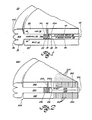
- a portion of a diode 20 includes a semiconductor wafer 22 in the form of a layer of silicon crystal material housed in a hermetically sealed, silicon package 24.
- Chip 22 includes an N-type cathode region 26 overlying a P-type anode region 28.
- package 24 includes an electrically conductive base 30, an electrically conductive cap 32, an electrically insulative sidewall 34, an electrical passivant 36 and an arc suppressant 38, each preferably comprising a silicon material.
- Base 30 comprises a layer of low-resistivity silicon material, preferably a highly-doped silicon, and is bonded to and disposed in electrical contact with anode region 28 of wafer 22 at a junction 40.
- Cap 32 also comprises a highly-doped, low-resistivity silicon, and is bonded to and disposed in electrical contact with cathode region 26 of wafer 22 at a junction 42.
- Cap 32 and base 30 each are preferably doped with P type dopants such as aluminum, boron or gallium, or N type dopants such as arsenic, phosphorous or antimony. The concentration of dopants is selected to provide cap 32 and base 30 with a low resistivity (on the order of 4 milli-ohm centimeters).
- junctions 40 and 42 each comprise a lead alloy solder, an aluminum-silicon alloy solder, or a diffusion bond.
- a preferred lead alloy solder comprises, for example, an alloy of 92.5% lead, 5% tin and 2.5% silver.
- a preferred diffusion bond is formed, in a manner well known in the art, by 1) sputtering copper on the mating surfaces, and 2) holding these surfaces in intimate contact at a high temperature.
- Sidewall 34 includes a layer portion 34a disposed between base 30 and cap 32 and an outer portion 34b surrounding package 24.
- Sidewall layer portion 34a surrounds wafer 22, includes an edge 34c spaced apart from an edge 22a of the wafer, and is bonded to cap 32 at a junction 48, and base 30 at a junction 50, so as to hermetically seal package 24.
- Sidewall outer portion 34b includes a three-lobed edge 34d surrounding the outside of package 24 and adjoining base 30 and cap 32.
- Sidewall 34 comprises pre-molded silicon glass selected to have a coefficient of thermal expansion close to that of silicon wafer 22.
- the coefficient of thermal expansion of silicon glass is controlled by selecting the quantity of additives, such as boron oxide (B2O3) or sodium monoxide (Na2O), which are added to the silicon glass.
- Junctions 48 and 50 are preferably formed using the solders or diffusion bond described above with respect to junctions 40 and 42, or by the use of glass frits.
- Passivant 36 is fabricated directly on edge 22a of wafer 22, and preferably comprises a polyimide, a silicone room-temperature vulcanizing rubber (RTV), or amorphous silicon.
- Arc suppressent 38 preferably comprising alumina (Al2O3), silicon dioxide (SiO2), or RTV, is disposed within package 24 between sidewall layer edge 34c and wafer edge 22.
- An aperture 52 shown sealed with a low temperature lead-tin eutectic, is disposed in cap 32 for inserting arc suppressant 38 into package 24.
- cap 32 serves as a cathode contact for diode 20, while base 30 serves as an anode contact for the diode.
- External electrical leads (not shown) are soldered directly to cap 32 or base 30, as required.
- Passivant 36 functions to control the electric field developed across the junction between cathode region 26 and anode region 28, thereby preventing electrical breakdown between cap 32 and base 30.
- Arc suppressant 38 functions to suppress arcing between cap 32 and base 30.
- Lobed edge 34d of outer sidewall portion 34b functions to increase the length of the current creep path, indicated by dashed line 54, between cap 32 and base 30 along the outside edge of the package. It will be appreciated that the shape of lobed edge 34b is only important in so far as it increases the length of current creep path 54.
- those components of package 24 which don't necessarily comprise silicon materials (i.e., the bonds at junctions 40, 42, 48 and 50, passivant 36 and arc suppressant 38) include only a small percentage by volume of the package and therefore don't noticeably affect the functional characteristics of the package.
- a hermetically sealed, compact semiconductor package 24 comprising substantially entirely silicon materials having coefficients of thermal expansion close in value to that of semiconductor wafer 22.
- Package 24 due to the nature of its structure, exhibits a high ratio of surface area to volume. This ratio, combined with the good thermal conductivity of the silicon package components, makes package 24 efficient to cool. Further, the package can be constructed using conventional semiconductor manufacturing techniques.
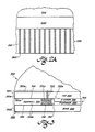
- Diode 220 is shown wherein features similar to those of Figure 1 retain like reference numerals incremented by 200.
- Diode 220 is substantially identical in structure to diode 20 of Figure 1 with the exception of the construction of cap 232 and base 230.
- cap 232 and base 230 each comprise a high-purity, high-resistivity silicon material including a plurality of vias 260 extending vertically (with respect to the view shown in Figures 2 and 2A) therethrough and into contact with cathode and anode regions 226 and 228, respectively.
- Each via 260 is filled with a conductive material 262, preferably comprising either an aluminum-silicon alloy, lead, or copper.
- vias 260 are fabricated to provide approximately 6 mil diameter holes located on 50 mil centers.
- the high-purity, high-resistivity silicon material comprising cap 232 and base 230 typically exhibits a higher coefficient of thermal conductivity than the highly-doped, low-resistivity silicon cap 30 and base 29 of Figure 1, providing package 220 with exceptionally good thermal conductivity.
- the conductive-material-filled vias 260 provide cap 232 and base 230 with very low electrical resistivity, i.e., on the order of 3 milli-ohm centimeters or less.
- package 224 still comprises substantially entirely silicon, and base 230 and cap 232 still retain substantially the same coefficient of thermal expansion as that of wafer 222.
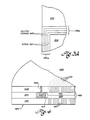
- Diode 320 is substantially identical in structure to diode 20 of Figure 1, with the exception of the construction of sidewall 334 and the inclusion of an insulating layer on cap 332 and base 330, the insulating layer being indicated at 332a and 330a, respectively.
- sidewall 334 comprises a layer of high-purity, high-resistivity silicon hermetically bonded to cap 332 at junction 348 and to base 330 at junction 350.
- An electrically insulative coating is disposed on the surface of the portions of cap 332 and base 330 extending outward beyond edge 322a of wafer 322, this coating being indicated at 330a and 332a, respectively.
- insulative coatings 330a and 332a each comprise alternating layers of semi-insulating polyoxygenated silicon (SIPOS) 360 and silicon dioxide (SiO2) 362.
- Junctions 348 and 350 are preferably formed using the solders, diffusion bonds or glass frits described hereinabove with respect to junctions 48 and 50.
- coatings 330a anbd 332a function to increase the distance of leakage current creep path 354 between base 330 and cap 332.
- the use of this insulative coating provides a more compact package.
- the use of high-purity silicon sidewall 334 provides a semiconductor package having a coefficient of thermal expansion closer in value to that of wafer 322.
- Diode 420 is shown wherein features similar to those of Figure 3 retain like reference numerals incremented by 100.
- Diode 420 is substantially identical to diode 320 of Figure 3 with the exception of the construction of cap 432 and base 430.
- cap 432 and base 430 are constructed substantially identically to cap 232 and base 230, respectively, of Figures 2 and 2A.
- Cap 432 and base 430 each comprise high-purity, high-resistivity silicon, and each includes a plurality of vias 460 extending vertically therethrough into contact with cathode and anode regions 426 and 428, respectively.
- each via 460 is filled with an electrically conductive material (not shown in detail in Figure 4) comprising either an aluminum-silicon alloy, lead, or copper.
- an electrically conductive material comprising either an aluminum-silicon alloy, lead, or copper.
- base 430 and cap 432 comprise high resistivity silicon, no insulative coating is required on their surfaces to provide a long leakage current creep path.
- the package shown and described in this embodiment of the invention provides the advantages of: compact size because side-lobes are not required on the sidewall, good thermal conductivity provided by the high-purity silicon cap, base and sidewall, and ease of construction because an insulative coating is not required on the cap and base.
- Diode 520 is substantially identical in structure to diode 220 of Figure 2 with the exception of the construction of sidewall 534 and its disposition on cap 532 and base 530.
- base 530 includes an edge 530a which extends laterally past an edge 522a of wafer 522. Edge 522a in turn extends laterally past an edge 532a of cap 532.
- Sidewall 534 comprises a layer of pre-molded silicon glass of the type described above, having a generally L-shaped cross-section including a leg 534a bonded to cap 532 at a junction 590 and a leg 534b bonded to base 530 at a junction 592, junctions 590 and 592 preferably being formed using the solders, diffusion bonds or glass frits described hereinabove.
- package 524 represents an alternative construction of package 224 ( Figure 2), and functions in a substantially identical manner.
- each embodiment is light in weight, compact in size, and provides a good thermal environment for the wafer. Further, each embodiment can be fabricated using known manufacturing technologies.
Landscapes
- Cooling Or The Like Of Semiconductors Or Solid State Devices (AREA)
- Structures Or Materials For Encapsulating Or Coating Semiconductor Devices Or Solid State Devices (AREA)
Applications Claiming Priority (2)
| Application Number | Priority Date | Filing Date | Title |
|---|---|---|---|
| US06/863,761 US4745455A (en) | 1986-05-16 | 1986-05-16 | Silicon packages for power semiconductor devices |
| US863761 | 1986-05-16 |
Publications (3)
| Publication Number | Publication Date |
|---|---|
| EP0246539A2 true EP0246539A2 (de) | 1987-11-25 |
| EP0246539A3 EP0246539A3 (en) | 1989-01-18 |
| EP0246539B1 EP0246539B1 (de) | 1993-07-28 |
Family
ID=25341730
Family Applications (1)
| Application Number | Title | Priority Date | Filing Date |
|---|---|---|---|
| EP87106854A Expired - Lifetime EP0246539B1 (de) | 1986-05-16 | 1987-05-12 | Silizium-Packungen für Leistungshalbleiteranordnungen |
Country Status (4)
| Country | Link |
|---|---|
| US (1) | US4745455A (de) |
| EP (1) | EP0246539B1 (de) |
| JP (1) | JP2526245B2 (de) |
| DE (1) | DE3786701T2 (de) |
Cited By (1)
| Publication number | Priority date | Publication date | Assignee | Title |
|---|---|---|---|---|
| EP0491389A1 (de) * | 1990-12-19 | 1992-06-24 | Siemens Aktiengesellschaft | Leistungshalbleiterbauelement |
Families Citing this family (14)
| Publication number | Priority date | Publication date | Assignee | Title |
|---|---|---|---|---|
| US4905075A (en) * | 1986-05-05 | 1990-02-27 | General Electric Company | Hermetic semiconductor enclosure |
| US5133795A (en) * | 1986-11-04 | 1992-07-28 | General Electric Company | Method of making a silicon package for a power semiconductor device |
| US4890156A (en) * | 1987-03-13 | 1989-12-26 | Motorola Inc. | Multichip IC module having coplanar dice and substrate |
| KR970007840B1 (ko) * | 1987-06-26 | 1997-05-17 | 미다 가쓰시게 | 반도체 장치 |
| US5034044A (en) * | 1988-05-11 | 1991-07-23 | General Electric Company | Method of bonding a silicon package for a power semiconductor device |
| US5209390A (en) * | 1989-07-03 | 1993-05-11 | General Electric Company | Hermetic package and packaged semiconductor chip having closely spaced leads extending through the package lid |
| US5412247A (en) * | 1989-07-28 | 1995-05-02 | The Charles Stark Draper Laboratory, Inc. | Protection and packaging system for semiconductor devices |
| US5223741A (en) * | 1989-09-01 | 1993-06-29 | Tactical Fabs, Inc. | Package for an integrated circuit structure |
| US5754403A (en) * | 1989-09-29 | 1998-05-19 | Texas Instruments Incorporated | Constraining core for surface mount technology |
| GB9014491D0 (en) * | 1990-06-29 | 1990-08-22 | Digital Equipment Int | Mounting silicon chips |
| US6867499B1 (en) | 1999-09-30 | 2005-03-15 | Skyworks Solutions, Inc. | Semiconductor packaging |
| JP3675364B2 (ja) * | 2001-05-30 | 2005-07-27 | ソニー株式会社 | 半導体装置用基板その製造方法および半導体装置 |
| TWM317648U (en) * | 2007-01-04 | 2007-08-21 | Lingsen Precision Ind Ltd | Package structure reducing noise interference |
| EP3382753A1 (de) * | 2017-03-30 | 2018-10-03 | Siemens Aktiengesellschaft | Isolation für eine mehrlagige elektrische schaltung und verfahren zur herstellung einer isolation |
Family Cites Families (10)
| Publication number | Priority date | Publication date | Assignee | Title |
|---|---|---|---|---|
| US3354258A (en) * | 1965-07-21 | 1967-11-21 | Hughes Aircraft Co | Package for semiconductor devices and method of making same |
| CH497790A (de) * | 1967-11-15 | 1970-10-15 | Mitsubishi Electric Corp | Halbleiterelement |
| GB1311659A (en) * | 1969-07-30 | 1973-03-28 | Secr Defence | Electrical device substrates |
| DE2014289A1 (de) * | 1970-03-25 | 1971-10-14 | Semikron Gleichrichterbau | Scheibenförmiges Halbleiterbauele ment und Verfahren zu seiner Herstellung |
| US3643136A (en) * | 1970-05-22 | 1972-02-15 | Gen Electric | Glass passivated double beveled semiconductor device with partially spaced preform |
| DE2364728A1 (de) * | 1973-12-27 | 1975-07-03 | Licentia Gmbh | Scheibenfoermiges halbleiterbauelement grosser leistungsfaehigkeit mit kunststoffummantelung |
| US3925808A (en) * | 1974-08-08 | 1975-12-09 | Westinghouse Electric Corp | Silicon semiconductor device with stress-free electrodes |
| US3996602A (en) * | 1975-08-14 | 1976-12-07 | General Instrument Corporation | Passivated and encapsulated semiconductors and method of making same |
| DE2937049A1 (de) * | 1979-09-13 | 1981-04-02 | Brown, Boveri & Cie Ag, 6800 Mannheim | Leistungs-halbleiterbauelement |
| US4630096A (en) * | 1984-05-30 | 1986-12-16 | Motorola, Inc. | High density IC module assembly |
-
1986
- 1986-05-16 US US06/863,761 patent/US4745455A/en not_active Expired - Lifetime
-
1987
- 1987-05-12 EP EP87106854A patent/EP0246539B1/de not_active Expired - Lifetime
- 1987-05-12 DE DE87106854T patent/DE3786701T2/de not_active Expired - Fee Related
- 1987-05-13 JP JP62114929A patent/JP2526245B2/ja not_active Expired - Lifetime
Cited By (1)
| Publication number | Priority date | Publication date | Assignee | Title |
|---|---|---|---|---|
| EP0491389A1 (de) * | 1990-12-19 | 1992-06-24 | Siemens Aktiengesellschaft | Leistungshalbleiterbauelement |
Also Published As
| Publication number | Publication date |
|---|---|
| EP0246539A3 (en) | 1989-01-18 |
| JPS62291052A (ja) | 1987-12-17 |
| JP2526245B2 (ja) | 1996-08-21 |
| EP0246539B1 (de) | 1993-07-28 |
| DE3786701D1 (de) | 1993-09-02 |
| US4745455A (en) | 1988-05-17 |
| DE3786701T2 (de) | 1994-01-05 |
Similar Documents
| Publication | Publication Date | Title |
|---|---|---|
| EP0246539A2 (de) | Silizium-Packungen für Leistungshalbleiteranordnungen | |
| US4249034A (en) | Semiconductor package having strengthening and sealing upper chamber | |
| US4267559A (en) | Low thermal impedance light-emitting diode package | |
| EP1596434B1 (de) | Halbleiterbauelement | |
| US7948069B2 (en) | Surface mountable hermetically sealed package | |
| EP3255686B1 (de) | Led-gehäusestruktur | |
| US5577656A (en) | Method of packaging a semiconductor device | |
| US4670771A (en) | Rectifier module | |
| KR101659103B1 (ko) | 반도체 소자를 위한 지지 몸체, 반도체 소자 및 지지 몸체의 제조 방법 | |
| US4905075A (en) | Hermetic semiconductor enclosure | |
| EP0114917A2 (de) | Halbleiterverkapselungen | |
| WO1988007761A1 (en) | Metal packages having improved thermal dissipation | |
| US20230260861A1 (en) | Semiconductor packages with increased power handling | |
| JPH0677357A (ja) | 改良された半導体パッケージ、集積回路デバイスをパッケージする改良された方法、および半導体デバイスを冷却する方法 | |
| CN104350617A (zh) | 发光装置 | |
| US4367523A (en) | Rectifier bridge unit | |
| US20030011053A1 (en) | Semiconductor device | |
| US20070200223A1 (en) | Semiconductor device and semiconductor module therewith | |
| EP0340466B1 (de) | Halbleiteranordnung mit Zuleitungen | |
| CN87104825A (zh) | 散热性能改善了的大规模集成电路封装 | |
| JP7721503B2 (ja) | 半導体装置 | |
| EP0244767A2 (de) | Hermetisches Halbleitergehäuse und Verfahren zum Herstellen | |
| EP1560266A2 (de) | Auf einer oberfläche montiertes hermetisches Leistungsgehäuse | |
| US5034044A (en) | Method of bonding a silicon package for a power semiconductor device | |
| US3590338A (en) | Light activated semiconductor device |
Legal Events
| Date | Code | Title | Description |
|---|---|---|---|
| PUAI | Public reference made under article 153(3) epc to a published international application that has entered the european phase |
Free format text: ORIGINAL CODE: 0009012 |
|
| AK | Designated contracting states |
Kind code of ref document: A2 Designated state(s): CH DE FR GB LI SE |
|
| PUAL | Search report despatched |
Free format text: ORIGINAL CODE: 0009013 |
|
| AK | Designated contracting states |
Kind code of ref document: A3 Designated state(s): CH DE FR GB LI SE |
|
| 17P | Request for examination filed |
Effective date: 19890703 |
|
| 17Q | First examination report despatched |
Effective date: 19920113 |
|
| GRAA | (expected) grant |
Free format text: ORIGINAL CODE: 0009210 |
|
| AK | Designated contracting states |
Kind code of ref document: B1 Designated state(s): CH DE FR GB LI SE |
|
| ET | Fr: translation filed | ||
| REF | Corresponds to: |
Ref document number: 3786701 Country of ref document: DE Date of ref document: 19930902 |
|
| PLBE | No opposition filed within time limit |
Free format text: ORIGINAL CODE: 0009261 |
|
| STAA | Information on the status of an ep patent application or granted ep patent |
Free format text: STATUS: NO OPPOSITION FILED WITHIN TIME LIMIT |
|
| 26N | No opposition filed | ||
| EAL | Se: european patent in force in sweden |
Ref document number: 87106854.0 |
|
| PGFP | Annual fee paid to national office [announced via postgrant information from national office to epo] |
Ref country code: FR Payment date: 19960415 Year of fee payment: 10 |
|
| PGFP | Annual fee paid to national office [announced via postgrant information from national office to epo] |
Ref country code: GB Payment date: 19960425 Year of fee payment: 10 |
|
| PG25 | Lapsed in a contracting state [announced via postgrant information from national office to epo] |
Ref country code: GB Effective date: 19970512 |
|
| PGFP | Annual fee paid to national office [announced via postgrant information from national office to epo] |
Ref country code: SE Payment date: 19970521 Year of fee payment: 11 |
|
| PGFP | Annual fee paid to national office [announced via postgrant information from national office to epo] |
Ref country code: DE Payment date: 19970522 Year of fee payment: 11 |
|
| PGFP | Annual fee paid to national office [announced via postgrant information from national office to epo] |
Ref country code: CH Payment date: 19970528 Year of fee payment: 11 |
|
| GBPC | Gb: european patent ceased through non-payment of renewal fee |
Effective date: 19970512 |
|
| PG25 | Lapsed in a contracting state [announced via postgrant information from national office to epo] |
Ref country code: FR Free format text: LAPSE BECAUSE OF NON-PAYMENT OF DUE FEES Effective date: 19980130 |
|
| REG | Reference to a national code |
Ref country code: FR Ref legal event code: ST |
|
| PG25 | Lapsed in a contracting state [announced via postgrant information from national office to epo] |
Ref country code: SE Free format text: LAPSE BECAUSE OF NON-PAYMENT OF DUE FEES Effective date: 19980513 |
|
| PG25 | Lapsed in a contracting state [announced via postgrant information from national office to epo] |
Ref country code: LI Free format text: LAPSE BECAUSE OF NON-PAYMENT OF DUE FEES Effective date: 19980531 Ref country code: CH Free format text: LAPSE BECAUSE OF NON-PAYMENT OF DUE FEES Effective date: 19980531 |
|
| REG | Reference to a national code |
Ref country code: CH Ref legal event code: PL |
|
| EUG | Se: european patent has lapsed |
Ref document number: 87106854.0 |
|
| PG25 | Lapsed in a contracting state [announced via postgrant information from national office to epo] |
Ref country code: DE Free format text: LAPSE BECAUSE OF NON-PAYMENT OF DUE FEES Effective date: 19990302 |