EP3255686B1 - Led-gehäusestruktur - Google Patents
Led-gehäusestruktur Download PDFInfo
- Publication number
- EP3255686B1 EP3255686B1 EP16199084.1A EP16199084A EP3255686B1 EP 3255686 B1 EP3255686 B1 EP 3255686B1 EP 16199084 A EP16199084 A EP 16199084A EP 3255686 B1 EP3255686 B1 EP 3255686B1
- Authority
- EP
- European Patent Office
- Prior art keywords
- light
- emitting unit
- led chip
- electrode
- region
- Prior art date
- Legal status (The legal status is an assumption and is not a legal conclusion. Google has not performed a legal analysis and makes no representation as to the accuracy of the status listed.)
- Active
Links
Images


Classifications
-
- H—ELECTRICITY
- H10—SEMICONDUCTOR DEVICES; ELECTRIC SOLID-STATE DEVICES NOT OTHERWISE PROVIDED FOR
- H10H—INORGANIC LIGHT-EMITTING SEMICONDUCTOR DEVICES HAVING POTENTIAL BARRIERS
- H10H20/00—Individual inorganic light-emitting semiconductor devices having potential barriers, e.g. light-emitting diodes [LED]
- H10H20/80—Constructional details
- H10H20/85—Packages
- H10H20/851—Wavelength conversion means
- H10H20/8514—Wavelength conversion means characterised by their shape, e.g. plate or foil
-
- H—ELECTRICITY
- H10—SEMICONDUCTOR DEVICES; ELECTRIC SOLID-STATE DEVICES NOT OTHERWISE PROVIDED FOR
- H10H—INORGANIC LIGHT-EMITTING SEMICONDUCTOR DEVICES HAVING POTENTIAL BARRIERS
- H10H20/00—Individual inorganic light-emitting semiconductor devices having potential barriers, e.g. light-emitting diodes [LED]
- H10H20/80—Constructional details
- H10H20/85—Packages
-
- G—PHYSICS
- G02—OPTICS
- G02B—OPTICAL ELEMENTS, SYSTEMS OR APPARATUS
- G02B5/00—Optical elements other than lenses
- G02B5/02—Diffusing elements; Afocal elements
- G02B5/0273—Diffusing elements; Afocal elements characterized by the use
- G02B5/0278—Diffusing elements; Afocal elements characterized by the use used in transmission
-
- H—ELECTRICITY
- H10—SEMICONDUCTOR DEVICES; ELECTRIC SOLID-STATE DEVICES NOT OTHERWISE PROVIDED FOR
- H10D—INORGANIC ELECTRIC SEMICONDUCTOR DEVICES
- H10D1/00—Resistors, capacitors or inductors
- H10D1/40—Resistors
- H10D1/47—Resistors having no potential barriers
-
- H—ELECTRICITY
- H10—SEMICONDUCTOR DEVICES; ELECTRIC SOLID-STATE DEVICES NOT OTHERWISE PROVIDED FOR
- H10D—INORGANIC ELECTRIC SEMICONDUCTOR DEVICES
- H10D8/00—Diodes
- H10D8/20—Breakdown diodes, e.g. avalanche diodes
- H10D8/25—Zener diodes
-
- H—ELECTRICITY
- H10—SEMICONDUCTOR DEVICES; ELECTRIC SOLID-STATE DEVICES NOT OTHERWISE PROVIDED FOR
- H10D—INORGANIC ELECTRIC SEMICONDUCTOR DEVICES
- H10D89/00—Aspects of integrated devices not covered by groups H10D84/00 - H10D88/00
- H10D89/60—Integrated devices comprising arrangements for electrical or thermal protection, e.g. protection circuits against electrostatic discharge [ESD]
-
- H—ELECTRICITY
- H10—SEMICONDUCTOR DEVICES; ELECTRIC SOLID-STATE DEVICES NOT OTHERWISE PROVIDED FOR
- H10H—INORGANIC LIGHT-EMITTING SEMICONDUCTOR DEVICES HAVING POTENTIAL BARRIERS
- H10H20/00—Individual inorganic light-emitting semiconductor devices having potential barriers, e.g. light-emitting diodes [LED]
- H10H20/80—Constructional details
- H10H20/84—Coatings, e.g. passivation layers or antireflective coatings
- H10H20/841—Reflective coatings, e.g. dielectric Bragg reflectors
-
- H—ELECTRICITY
- H10—SEMICONDUCTOR DEVICES; ELECTRIC SOLID-STATE DEVICES NOT OTHERWISE PROVIDED FOR
- H10H—INORGANIC LIGHT-EMITTING SEMICONDUCTOR DEVICES HAVING POTENTIAL BARRIERS
- H10H20/00—Individual inorganic light-emitting semiconductor devices having potential barriers, e.g. light-emitting diodes [LED]
- H10H20/80—Constructional details
- H10H20/85—Packages
- H10H20/8506—Containers
-
- H—ELECTRICITY
- H10—SEMICONDUCTOR DEVICES; ELECTRIC SOLID-STATE DEVICES NOT OTHERWISE PROVIDED FOR
- H10H—INORGANIC LIGHT-EMITTING SEMICONDUCTOR DEVICES HAVING POTENTIAL BARRIERS
- H10H20/00—Individual inorganic light-emitting semiconductor devices having potential barriers, e.g. light-emitting diodes [LED]
- H10H20/80—Constructional details
- H10H20/85—Packages
- H10H20/852—Encapsulations
-
- H—ELECTRICITY
- H10—SEMICONDUCTOR DEVICES; ELECTRIC SOLID-STATE DEVICES NOT OTHERWISE PROVIDED FOR
- H10H—INORGANIC LIGHT-EMITTING SEMICONDUCTOR DEVICES HAVING POTENTIAL BARRIERS
- H10H20/00—Individual inorganic light-emitting semiconductor devices having potential barriers, e.g. light-emitting diodes [LED]
- H10H20/80—Constructional details
- H10H20/85—Packages
- H10H20/855—Optical field-shaping means, e.g. lenses
- H10H20/856—Reflecting means
-
- H—ELECTRICITY
- H10—SEMICONDUCTOR DEVICES; ELECTRIC SOLID-STATE DEVICES NOT OTHERWISE PROVIDED FOR
- H10H—INORGANIC LIGHT-EMITTING SEMICONDUCTOR DEVICES HAVING POTENTIAL BARRIERS
- H10H20/00—Individual inorganic light-emitting semiconductor devices having potential barriers, e.g. light-emitting diodes [LED]
- H10H20/80—Constructional details
- H10H20/85—Packages
- H10H20/857—Interconnections, e.g. lead-frames, bond wires or solder balls
-
- H—ELECTRICITY
- H10—SEMICONDUCTOR DEVICES; ELECTRIC SOLID-STATE DEVICES NOT OTHERWISE PROVIDED FOR
- H10H—INORGANIC LIGHT-EMITTING SEMICONDUCTOR DEVICES HAVING POTENTIAL BARRIERS
- H10H20/00—Individual inorganic light-emitting semiconductor devices having potential barriers, e.g. light-emitting diodes [LED]
- H10H20/80—Constructional details
- H10H20/85—Packages
- H10H20/858—Means for heat extraction or cooling
- H10H20/8582—Means for heat extraction or cooling characterised by their shape
-
- H10W72/536—
-
- H10W72/5363—
-
- H10W72/5434—
-
- H10W90/00—
Definitions
- the instant invention relates to an LED package structure; in particular, to a light-emitting unit of an LED package structure including an LED chip, a fluorescent body and the additional features defined in the independent claims.
- the conventional LED package structure includes a substrate, a circuit layer disposed on the substrate, an LED chip mounted on the circuit layer, and a fluorescent body covering the LED chip.
- the fluorescent body also covers the circuit layer, such that an electrical error due to a die bonding area covered by the fluorescent body is easily generated between the LED chip and the circuit layer.
- EP 2 884 549 A1 relates to a small and thin light-emitting device, which is a side view type light-emitting device, including a base body including a base material having a pair of connection terminals on at least a first main surface; a light-emitting element connected to the connection terminals; and a sealing member that seals the light-emitting element, wherein the base material has a linear expansion coefficient within ⁇ 10 ppm/°C of the linear expansion coefficient of the light-emitting element.
- WO 2012/164431 A1 relates to a wafer scale process for attaching a semiconductor light emitting device to a support substrate.
- US 2015/311405 A1 relates to an LED device that lends itself to chip size packaging, and yet has a good light-emitting efficiency and is capable of providing a confined light distribution and a method for manufacturing the same.
- LED package structure according to the prior art is also disclosed in US2015041845 A1 .
- the invention provides an LED package structure according to any of independent claims 1 and 11 for effectively solving the problem generated from the conventional LED package structure. Further embodiments of the invention are described in the respective dependent claims.
- the light-emitting unit of the LED package structure of the instant disclosure is disposed on the substrate and the fluorescent body of the light-emitting unit spaced apart from the circuit layer with the gap in a range of 3 ⁇ m ⁇ 10 ⁇ m.
- the gap is filled with the reflective housing (or the light transparent layer), such that the electrical connection between the light-emitting unit and the circuit layer is not influenced by the fluorescent body, thereby the poor electrical connection can be improved.
- the top plane of the reflective housing is equal to that of the light-emitting unit, or the top plane of the reflective housing is lower than that of the light-emitting unit, and the distance between the two top planes is zero or in a range of 1 ⁇ 30 ⁇ m, and include the additional features as defined in the independent claims, thus problems about light shape and poor brightness can be avoided.
- FIGs. 1 through 11D show a first embodiment of the invention. References are hereunder made to the detailed descriptions and appended drawings in connection with the instant invention. However, the appended drawings are merely shown for exemplary purposes, rather than being used to restrict the scope of the instant invention as defined in the appended claims.
- the designs of light-emitting units 5 illustrated by Figures 6A, 6B, 6C, 6D , 6E, 6F , 6H , and 6J do not comprise all features of anyone of the independent claims.
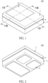
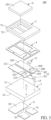
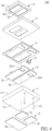
- the LED package structure 100 includes a substrate 1, a circuit layer 2, a soldering pad 3, an insulating layer 4, a light-emitting unit 5, a Zener diode chip 6, and a reflective housing 7 integrally formed with the insulating layer 4.
- the circuit layer 2 and the soldering pad 3 are respectively disposed on two opposite surfaces of the substrate 1.
- the insulating layer 4 is disposed on the substrate 1 and is shaped complementarily with the circuit layer 2.
- the light-emitting unit 5 and the Zener diode chip 6 are both disposed on the circuit layer 2 and the insulating layer 4.
- the substrate 1 having a substantially rectangular shape includes a first surface 11 and a second surface 12 opposing to the first surface 11.
- the substrate 1 includes two conductive pillars 13 embedded therein, and two opposite ends of each conductive pillar 13 are respectively exposed from the first surface 11 and the second surface 12.
- the circuit layer 2 is disposed on the first surface 11 of the substrate 1, and the soldering pad 3 is disposed on the second surface 12 of the substrate 1.
- the circuit layer 2 includes a first electrode 21 and a second electrode 22 spaced apart from the first electrode 21.
- the first electrode 21 and the second electrode 22 are substantially in a mirror symmetry, but the instant disclosure is not limited thereto.
- the first electrode 21 includes a first bonding region 211, a first extending region 212, and a first connecting region 213 connected to the first bonding region 211 and the first extending region 212.
- the first bonding region 211, the first extending region 212, and the first connecting region 213 are arranged in a direction parallel to a longitudinal direction of the substrate 1.
- the area of the first bonding region 211 is greater than that of the first extending region 212, and the area of the first extending region 212 is greater than that of the first connecting region 213.
- the second electrode 22 includes a second bonding region 221, a second extending region 222, and a second connecting region 223 connected to the second bonding region 221 and the second extending region 222.
- the second bonding region 221, the second extending region 222, and the second connecting region 223 are arranged in a direction parallel to the longitudinal direction of the substrate 1.
- the area of the second bonding region 221 is greater than that of the second extending region 222, and the area of the second extending region 222 is greater than that of the second connecting region 223.
- the second bonding region 221, the second extending region 222, and the second connecting region 223 are respectively arranged adjacent to the first bonding region 211, the first extending region 212, and the first connecting region 213.
- a distance D1 between the first bonding region 211 and the second bonding region 221 is greater than a distance D2 between the first extending region 212 and the second extending region 222.
- the distance D1 between the first bonding region 211 and the second bonding region 221 is corresponding to (i.e., substantially identical to) a distance between two chip electrodes 511 of the light-emitting unit 5. That is to say, the distance D1 can be changed according to the distance between two chip electrodes 511 of the light-emitting unit 5.
- the distance D2 between the first extending region 212 and the second extending region 222 is corresponding to (i.e., substantially identical to) a distance between two chip electrodes (not labeled) of the Zener diode chip 6. That is to say, the distance D2 can be changed according to the distance between two chip electrodes of the Zener diode chip 6.
- each of the light-emitting unit 5 and the Zener diode chip 6 can be mounted on the first electrode 21 and the second electrode 22 for the purpose of reducing the size of the circuit layer 2.
- the adjacent inner edges of the first bonding region 211 and the second bonding region 221 are parallel to each other and the distance D1 between the first bonding region 211 and the second bonding region 221 is in a range of 150 ⁇ m ⁇ 200 ⁇ m (i.e., 150 ⁇ m is a preferable value), the adjacent inner edges of the first extending region 212 and the second extending region 222 are parallel to each other and the distance D2 between the first extending region 212 and the second extending region 222 is in a range of 90 ⁇ m ⁇ 150 ⁇ m (i.e., 90 ⁇ m is a preferable value), and a distance between the adjacent inner edges of the first connecting region 213 and the second connecting region 223 is gradually decreased in a direction from the distance D1 to the distance D2 (i.e., the distance between the adjacent inner edges of the first connecting region 213 and the second connecting region 223 gradually decreases from 150 ⁇ m to 90 ⁇ m).
- the instant disclosure is not limited to the above conditions.
- a U-shaped first notch 214 is defined by the first bonding region 211, the first connecting region 213, and the first extending region 212.
- a U-shaped second notch 224 is defined by the second bonding region 221, the second connecting region 223, and the second extending region 222.
- An opening of the first notch 214 and an opening of the second notch 224 respectively face toward two sides away from each other in a width direction of the substrate 1, such that an area of the circuit layer 2 covering the first surface 11 of the substrate 1 can be reduced, thereby increasing an area of the insulating layer 4 covering the first surface 11 of the substrate 1. Accordingly, the insulating layer 4 and the substrate 1 are provided with a better combination performance to prevent the reflective housing 7 from peeling off during in a manufacturing process and to prevent the reflective housing 7 from cracks during a sawing process.
- the soldering pad 3 includes two electrode soldering pads 31 and a heat-dissipating soldering pad 32.
- the two electrode soldering pads 31 are electrically connected to the circuit layer 2, and the two electrode soldering pads 31 are electrically connected to the light-emitting unit 5 through the circuit layer 2.
- an area of each electrode soldering pad 31 is smaller than that of the heat-dissipating soldering pad 21, and the area of each electrode soldering pad 31 in the instant embodiment is smaller than half of the area of the heat-dissipating soldering pad 21, but the instant disclosure is not limited thereto.
- the two electrode soldering pads 31 are respectively arranged under the first extending region 212 and the second extending region 222, and the two electrode soldering pads 31 are respectively and electrically connected to the first extending region 212 and the second extending region 222 through the two conductive pillars 13.
- the heat-dissipating soldering pad 32 is arranged on one side of the two electrode soldering pads 31 and is under the first bonding region 211 and the second bonding region 221 (or is under the LED chip 51) for dissipating heat generated from the light-emitting unit 5.
- the insulating layer 4 is disposed on the first surface 11 of the substrate 1, and the insulating layer 4 and the circuit layer 2 are shaped complementarily. That is to say, the insulating layer 4 and the circuit layer 2 are coplanar and are arranged with a complementary shape. In other words, the insulating layer 4 is disposed on a portion of the first surface 11, which is not disposed with the circuit layer 2, and the side edge of the insulating layer 4 is aligned with the side edge of the substrate 1. Thus, a portion of the insulating layer 4 is arranged between the first electrode 21 and the second electrode 22 such that a current leakage can be prevented between the first electrode 21 and the second electrode 22 of the circuit layer 2.
- the light-emitting unit 5 in the instant embodiment is a chip scale package (CSP) and includes an LED chip 51 and a fluorescent body 52 encapsulating the LED chip 51.
- the fluorescent body 52 encapsulates a top surface and a side surface of the LED chip 51.
- the relationship of the LED chip 51 and the fluorescent body 52 can be changed according to the designer's demand, such as the light-emitting unit 5 shown in Figs. 6A through 6E , wherein the light-emitting units 5 shown in Figs. 6D and 6E do not form part of the claimed invention, or the light-emitting unit 5 having a reflecting cup 53 at least surrounded a side surface 513 of the LED chip 51, shown in Figs.
- the fluorescent body 52 encapsulates a top surface 512 of the LED chip 51 and a side surface 513 of the LED chip 51 and exposes the two chip electrodes 511 arranged on a bottom of the LED chip 51, and a bottom surface 523 of the fluorescent body 52 is coplanar with a bottom surface 514 of the LED chip 51.
- the top surface 521 of the fluorescent body 52 (i.e., the top plane 521) is parallel to the top surface 512 of the LED chip 51, a side surface 522 of the fluorescent body 52 is parallel to the side surface 513 of the LED chip 51, and a smallest distance D3 between the top surface 521 of the fluorescent body 52 and the top surface 512 of the LED chip 51 is in a range of 50 ⁇ m ⁇ 200 ⁇ m, but the instant disclosure is not limited thereto.
- a light leakage of the LED chip 51 can be improved by using the fluorescent body 52 to encapsulate the top surface 512 and the side surface 513 of the LED chip 51.
- the fluorescent body 52 encapsulates the top surface 512 of the LED chip 51 and the side surface 513 of the LED chip 51 and exposes the two chip electrodes 511 arranged on the bottom of the LED chip 51, and a bottom edge of the fluorescent body 52 is aligned with the bottom surface 514 of the LED chip 51.
- the top surface 521 of the fluorescent body 52 is parallel to the top surface 512 of the LED chip 51, and the side surface 522 of the fluorescent body 52 is non-parallel to the side surface 513 of the LED chip 51.
- the top surface 521 and the side surface 522 of the fluorescent body 52 have an acute angle
- the side surface 522 of the fluorescent body 52 and the side surface 513 of the LED chip 51 have an acute angle.
- the fluorescent body 52 encapsulates the top surface 512 of the LED chip 51 and the side surface 513 of the LED chip 51 and exposes the two chip electrodes 511 arranged on the bottom of the LED chip 51, and a bottom edge of the fluorescent body 52 is aligned with the bottom surface 514 of the LED chip 51.
- the top surface 521 of the fluorescent body 52 is parallel to the top surface 512 of the LED chip 51.
- the side surface 522 of the fluorescent body 52 includes a first side surface 5221 and a second side surface 5222.
- the first side surface 5221 and the top surface 521 of the fluorescent body 52 have a right angle
- the first side surface 5221 and the second side surface 5222 have an obtuse angle
- the second side surface 5222 of the fluorescent body 52 and the side surface 513 of the LED chip 51 have an acute angle
- the fluorescent body 52 encapsulates the top surface 512 of the LED chip 51 and part (i.e., the upper part) of the side surface 513 of the LED chip 51, and the fluorescent body 52 exposes the two chip electrodes 511 arranged on the bottom of the LED chip 51 and the other part (i.e., the lower part) of the side surface 513 of the LED chip 51.
- the top surface 521 of the fluorescent body 52 is parallel to the top surface 512 of the LED chip 51.
- the side surface 522 of the fluorescent body 52 includes a first side surface 5221 and a second side surface 5222.
- the first side surface 5221 and the top surface 521 of the fluorescent body 52 have a right angle
- the first side surface 5221 and the second side surface 5222 have an obtuse angle
- the second side surface 5222 of the fluorescent body 52 and the side surface 513 of the LED chip 51 have an acute angle.
- the fluorescent body 52 is a phosphor sheet, and the top surface 521 of the fluorescent body 52 is longer than the top surface 512 of the LED chip 51.
- the fluorescent body 52 only covers the top surface 512 of the LED chip 51, and the fluorescent body 52 exposes the two chip electrodes 511 arranged on the bottom of the LED chip 51 and the side surface 513 of the LED chip 51.
- the top surface 521 of the fluorescent body 52 is parallel to the top surface 512 of the LED chip 51.
- the bottom surface 523 of the fluorescent body 52 is coplanar with the top surface 512 of the LED chip 51.
- the light-emitting unit 5 further includes a reflecting cup 53 formed on the side surface 513 of the LED chip 51.
- a top surface 531 of the reflecting cup 53 is coplanar with the top surface 512 of the LED chip 51, and a bottom surface 533 of the reflecting cup 53 is coplanar with the bottom surface 514 of the LED chip 51.
- the fluorescent body 52 is disposed on the top surface 531 of the reflecting cup 53 and the top surface 512 of the LED chip 51, and the side surface 522 of the fluorescent body 52 is coplanar with a side surface 532 of the reflecting cup 53.
- the light-emitting unit 5 further includes a reflecting cup 53 formed on the side surface 522 of the fluorescent body 52.
- the top surface 531 of the reflecting cup 53 is coplanar with the top surface 521 of the fluorescent body 52.
- the bottom surface 533 of the reflecting cup 53 is coplanar with the bottom surface 523 of the fluorescent body 52 and the bottom surface 514 of the LED chip 51.
- the light-emitting unit 5 further includes a reflecting cup 53 formed on the side surface 522 of the fluorescent body 52 and the side surface 513 of the LED chip 51.
- the top surface 531 of the reflecting cup 53 is coplanar with the top surface 521 of the fluorescent body 52.
- the bottom surface 533 of the reflecting cup 53 is coplanar with the bottom surface 514 of the LED chip 51.
- the light-emitting unit 5 further includes a reflecting cup 53 formed on the side surface 522 of the fluorescent body 52.
- the top surface 531 of the reflecting cup 53 is coplanar with the top surface 521 of the fluorescent body 52.
- the bottom surface 533 of the reflecting cup 53 is coplanar with the bottom surface 514 of the LED chip 51.
- An inner wall 534 of the reflecting cup 53 is a two-stage wall having a first inner wall 5341 and a second inner wall 5342.
- the first inner wall 5341 of the reflecting cup 53 is entirely contacted with the first side surface 5221 of the fluorescent body 52
- the second inner wall 5342 of the reflecting cup 53 is entirely contacted with the second side surface 5222 of the fluorescent body 52.
- the light-emitting unit 5 further includes a transparent body 54 at least surrounded the side surface 513 of the LED chip 51.
- a top surface of the transparent body 54 is coplanar with the top surface 512 of the LED chip 51.
- the fluorescent body 52 is disposed on the top surface 512 of the LED chip 51 and the top surface of the transparent body 54, and the reflecting cup 53 is arranged outside the fluorescent body 52 and the transparent body 54.
- the top surface 531 of the reflecting cup 53 is coplanar with the top surface 521 of the fluorescent body 52.
- the bottom surface 533 of the reflecting cup 53 is coplanar with the bottom surface 514 of the LED chip 51.
- An inner wall 534 of the reflecting cup 53 is a two-stage wall having a first inner wall 5341 and a second inner wall 5342.
- the first inner wall 5341 of the reflecting cup 53 is entirely contacted with the side surface 522 of the fluorescent body 52, and the second inner wall 5342 of the reflecting cup 53 is entirely connected to the side surface of the transparent body 54.
- the LED chip 51 has a thickness of about 150 ⁇ m, the smallest distance D3 (shown in Fig. 6B ) between the top surface 512 of the LED chip 51 and the top surface 521 of the fluorescent body 52 is in a range of 100 ⁇ m ⁇ 180 ⁇ m, and a side portion of the fluorescent body 52 extended out of the top surface 512 of the LED chip 51 has a length in a range of 50 ⁇ m ⁇ 150 ⁇ m.
- the light-emitting unit 5 is mounted on the circuit layer 2 and the insulating layer 4, and the fluorescent body 52 is spaced apart from the insulating layer 4 (shown in Fig. 9 ).
- the two chip electrodes 511 of the LED chip 51 are respectively mounted on the first bonding region 211 and the second bonding region 221.
- the Zener diode chip 6 is in a flip chip manner, and the two chip electrodes of the Zener diode chip 6 are respectively mounted on the first extending region 212 and the second extending region 222, but the instant disclosure is not limited thereto.
- the Zener diode chip 6 can be in a wire-bonding manner, so that the Zener diode chip 6 is mounted on the first extending region 212 and is electrically connected to the second extending region 222 by wire-bonding; or the Zener diode chip 6 is mounted on the second extending region 222 and is electrically connected to the first extending region 212 by wire-bonding.
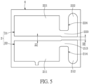
- the fluorescent body 52 is spaced apart from the circuit layer 2 with a gap G (as shown in Fig. 9 ) having a range of 3 ⁇ m ⁇ 10 ⁇ m, such that the electrical connection between the light-emitting unit 5 and the circuit layer 2 is not influenced by the fluorescent body 52, thereby poor electrical connection can be improved.
- the reflective housing 7 is disposed on the insulating layer 4.
- the material of the reflective housing 7 in the instant embodiment is identical to that of the insulating layer 4 (i.e., white silicone resin), and the reflective housing 7 and the insulating layer 4 are integrally formed in one piece.
- the reflective housing 7 in the instant embodiment is configured to reflect at least 80% of light emitted from the light-emitting unit 5, but the instant disclosure is not limited thereto.
- the reflective housing 7 is disposed on the insulating layer 4 and the circuit layer 2 to surround the light-emitting unit 5, and the gap G is further filled within the reflective housing 7 (as shown in Fig. 9 ), such that the reflective housing 7 covers the side surface of the light-emitting unit 5, a side surface 5111 of each chip electrode 511 of the light-emitting unit 5, and the bottom surface 523 of the fluorescent body 52, and the Zener diode chip 6 is embedded in the reflective housing 7.
- the reflective housing 7 includes a top plane 71 and an outer lateral surface 72.
- a distance between the top plane 71 of the reflective housing 7 and the first surface 11 of the substrate 1 is less than or equal to a distance between the top plane 521 of the light-emitting unit 5 and the first surface 11 of the substrate 1. That is to say, the top plane 71 of the reflective housing 7 is substantially lower than or equal to the top plane 521 of the light-emitting unit 5.
- a distance D4 (shown in Fig. 9 ) between the two top planes 71, 521 is zero or in a range of 1 ⁇ 30 ⁇ m (i.e., 0 ⁇ 30 ⁇ m).
- the two top planes 71, 521 in the instant embodiment are parallel to each other, and the distance D4 between the two top planes 71, 521 is preferably in a range of 15 ⁇ m ⁇ 30 ⁇ m, but the instant disclosure is not limited thereto.
- the outer lateral surface 72 of the reflective housing 7 is aligned with the side edge of the substrate 1 and the side edge of the insulating layer 4.
- a smallest distance D5 (shown in Fig. 7 ) between the outer lateral surface 72 of the reflective housing 7 and the side surface of the light-emitting unit 5 is more than or equal to 100 ⁇ m, and the smallest distance D5 is preferably in a range of 100 ⁇ m ⁇ 150 ⁇ m.
- the forward light efficiency of the light-emitting unit 5 can be effectively increased and the yellow ring and blue ring can be avoided by forming the reflective housing 7.
- the Zener diode chip 6 is embedded in the reflective housing 7, such that the light efficiency of the LED package structure 100 is not influenced by the Zener diode chip 6.
- the LED package structure 100 in the instant embodiment can further include a light diffusion layer 8 disposed on the reflective housing 7 and the fluorescent body 52.
- the light diffusion layer 8 in the instant embodiment is disposed on the top plane 521 of the fluorescent body 52 and the top plane 71 of the reflective housing 7.
- a thickness D6 of the light diffusion layer 8 is less than or equal to 50 ⁇ m, and the light diffusion layer 8 includes silica or titanium dioxide having a weight percent of 2 wt% ⁇ 5 wt%, but the instant disclosure is not limited thereto.
- the color uniformity of the LED package structure 100 can be effectively increased by disposing the light diffusion layer 8.
- Figs. 11A through 11D show the steps S 110 through S150 of the manufacturing method.
- the detailed relationship between the components of the LED package structure 100 has been disclosed in the above description, so the following description does not state it again.
- Step S110 as shown in Figs. 11A and 11B , a plurality of circuit layers 2 are disposed on a surface of a substrate assembly 10, a plurality of soldering layers 3 (not shown in Figs. 11A and 11B ) are disposed on an opposite surface of the substrate assembly 10, a plurality of light-emitting units 5 are respectively mounted on the circuit layers 2, and a plurality of Zener diode chips 6 are respectively mounted on the circuit layers 2.
- the substrate assembly 10 is a construction having a plurality of substrates 1 integrally connected with each other.
- Step S130 as shown in Figs. 11B and 11C , an insulating assembly 40 and a reflective housing assembly 70 are formed on the substrate assembly 10 by a molding manner to cover the circuit layers 2, the Zener diode chips 6, and the side surfaces of the light-emitting units 5. A top plane 521 of each light-emitting unit 5 is exposed from the reflective housing assembly 70.
- the insulating assembly 40 is a construction having a plurality of insulating layers 4 integrally connected with each other.
- the reflective housing assembly 70 is a construction having a plurality of reflective housings 7 integrally connected with each other.
- the insulating assembly 40 and the reflective housing assembly 70 can be formed in one-step manufacturing process or can be formed in two-step manufacturing processes.
- Step S150 as shown in Figs. 11C and 11D , the reflective housing assembly 70, the insulating assembly 40, and the substrate assembly 10 are sawed into a plurality of LED package structures 100.
- the figures corresponding to the manufacturing method show four LED package structures 100 for example, but the instant disclosure is not limited thereto.
- FIGs. 12 through 16 show a second embodiment.
- the second embodiment is similar to the first embodiment, and the identical features are not disclosed again.
- the different features between the two embodiments are disclosed as follows.
- the LED package structure 100 of the instant embodiment is formed without the Zener diode chip 6.
- the substrate 1 having a substantially square shape includes a ceramic layer 14 and two varistor layers 15 respectively disposed on two opposite surfaces of the ceramic layer 14. In a non-shown embodiment, only one varistor layer 15 is disposed on one side of the ceramic layer 14.
- Each of the conductive pillars 13 has a first conductive pillar 131 and two second conductive pillars 132 integrally connected to two opposite ends of the first conductive pillar 131 (as shown in Fig. 16 ).
- Each of the two first conductive pillars 131 is embedded in the ceramic layer 14 and is electrically connected to the circuit layer 2 and the soldering pad 3 by using the corresponding second conductive pillars 132.
- Two of the second conductive pillars 132 are respectively embedded in one of the two varistor layers 15 and are connected to the circuit layer 2, and the other two second conductive pillars 132 are embedded in the other varistor layer 15 and are connected to the soldering pad 3.
- Each of the varistor layers 15 includes at least two metallic layers 151 connected to the two second conductive pillars 132 embedded therein to have a capacitive effect.
- the material of each varistor layer 15 includes zine oxide, and the metallic layer 151 can be made of silver, gold, copper, nickel, palladium, and so on.
- the substrate 1 provided by the instant embodiment has a ESD function, which is identical to the Zener diode chip 6, such that the Zener diode chip 6 can be omitted to reduce the size of the LED package structure 100.
- the circuit layer 2 is disposed on the first surface 11 of the substrate 1 and includes a first electrode 21 and a second electrode 22.
- Each of the first electrode 21 and the second electrode 22 has a substantially rectangular shape.
- the soldering pad 3 is disposed on the second surface 12 of the substrate 1 and includes two electrode soldering pads 31 each having a substantially rectangular shape.
- a longitudinal direction of each electrode soldering pad 31 is substantially perpendicular to that of each of the first electrode 21 and the second electrode 22, such that a warpage problem, which may be easily happened due to the components having different coefficients of thermal expansion (CTE), can be avoided during the manufacturing process of the LED package structure 100.
- CTE coefficients of thermal expansion
- the two conductive pillars 13 are respectively embedded in two diagonal portions of the substrate 1, and the first electrode 21 and the second electrode 22 are respectively and electrically connected to the two electrode soldering pads 31 by using the two conductive pillars 13.
- the light-emitting unit 5 is mounted on the circuit layer 2, and the two chip electrodes 511 of the light-emitting unit 5 are respectively and electrically connected to the first electrode 21 and the second electrode 22.
- a center of the light-emitting unit 5 is substantially arranged at a central axis of the substrate 1 of the LED package structure 100. In other words, the light-emitting unit 5 in the instant embodiment is located at an optical center of the LED package structure 100.
- the insulating layer 4 and the reflective housing 7 are made of the same material and are integrally formed in one piece.
- the reflective housing 7 is arranged around the side surface of the light-emitting unit 5, and the outer lateral surface 72 of the reflective housing 7 is coplanar with the side surface of the substrate 1.
- the outer lateral surface 72 of the reflective housing 7 and the side surface 513 of the light-emitting unit 5 are parallel to each other and the distance D5 is formed there-between.
- the distance D5 between the outer lateral surface 72 of the reflective housing 7 and the side surface 513 of the light-emitting unit 5 is more than or equal to 100 ⁇ m and is preferably in a range of 100 ⁇ m ⁇ 500 ⁇ m.
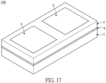
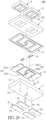
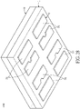
- FIGs. 17 through 22 show a third embodiment.
- the third embodiment is similar to the first embodiment, and the identical features are not disclosed again.
- the different features between the two embodiments are disclosed as follows.
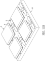
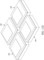
- the LED package structure 100 includes two light-emitting units 5 and two Zener diode chips 6. As shown in Figs. 17 through 20 , the circuit layer 2 is disposed on the first surface 11 of the substrate 1, and the circuit layer 2 has a 2-fold rotational symmetry along a central axis perpendicular to the substrate 1.
- the circuit layer 2 includes two first electrodes 21 and two second electrodes 22 arranged at an inner side the two first electrodes 21.
- Each of the two first electrodes 21 includes an L-shaped construction having a first bonding region 211 and a first extending region 212 perpendicularly connected to the first bonding region 211.
- Each of the two second electrodes 22 includes an L-shaped construction having a second bonding region 221 and a second extending region 222 perpendicularly connected to the second bonding region 221.
- the L-shaped constructions of the two first electrodes 21 have two corners respectively in position corresponding to two diagonal corners of the substrate 1, and the L-shaped constructions of the two second electrodes 22 have two corners respectively arranged at an inner side of the two corners of the two first electrodes 21.
- the second extending region 222 of each second electrode 22 is partially arranged at the inner corner of the other second electrode 22.
- a distance D1 between each first bonding region 211 and the adjacent second bonding region 221 is greater than a distance D2 between each first extending region 212 and the adjacent second extending region 222.
- the distance D1 between each of the first bonding regions 211 and the second bonding regions 221 is substantially in a range of 90 ⁇ m ⁇ 150 ⁇ m (i.e., 90 ⁇ m)
- the distance D2 between each of the first extending regions 212 and the second extending regions 222 is substantially in a range of 150 ⁇ m ⁇ 200 ⁇ m (i.e., 150 ⁇ m), but the instant disclosure is not limited thereto.
- the two light-emitting units 5 having different color temperature are disposed on the circuit layer 2 and the insulating layer 4 of the substrate 1.
- one of the two light-emitting units 5 has a warm color temperature of 1500K ⁇ 4000K
- the other one of the two light-emitting unit 5 has a cool color temperature of 4000K - 9000K, such that the LED package structure 100 can be prepared with a warm color temperature and a cool color temperature.
- the first bonding regions 211 and the second bonding regions 221 are in pair and are configured to connect with the two light-emitting units 5.
- the distance D7 between the two light-emitting units 5 is in a range of 0.1mm ⁇ 0.5mm and is preferably in a range of 0.3mm ⁇ 0.5mm.
- the distance D7 between the two light-emitting units 5 in the instant embodiment is 0.45mm, but it is not limited thereto.
- the first extending regions 212 and the second extending regions 222 are in pair and are configured to connect with the Zener diode chips 6.
- Each of the Zener diode chips 6 can be in a flip chip manner or in a vertical chip manner, and the instant disclosure is not limited thereto.
- the soldering pad 3 is disposed on the second surface 12 of the substrate 1 and includes two groups of electrode soldering pads 31.
- the soldering pad 3 is electrically connected to the circuit layer 2 by using the four conductive pillars 13.
- the two electrode soldering pads 31 of each group are respectively and electrically connected to the adjacent first electrode 21 and the adjacent second electrode 22.
- the two groups of electrode soldering pads 31 are respectively and electrically connected to the two light-emitting units 5 through the circuit layer 2. Accordingly, the LED package structure 100 is provided for the user with a plurality of operating modes by using the two groups of electrode soldering pads 31 to control the two light-emitting units 5.
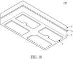
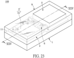
- FIGs. 23 through 26 show a fourth embodiment.
- the fourth embodiment is similar to the third embodiment, and the identical features are not disclosed again.
- the different features between the two embodiments are disclosed as follows.
- the instant embodiment uses a light transparent layer 9 to replace the insulating layer 4 and the reflective housing 7 of the third embodiment, and uses a auxiliary light-emitting unit 5' to replace one of the light-emitting units 5 of the third embodiment.
- the auxiliary light-emitting unit 5' in the instant embodiment is mounted on the circuit layer 2.
- the auxiliary light-emitting unit 5' in the instant embodiment is a UV LED chip 51', but the instant disclosure is not limited thereto.
- the light transparent layer 9 is disposed on the first surface 11 of the substrate 1 to encapsulate the light-emitting unit 5 and the auxiliary light-emitting unit 5' and is filled within the gap between the light-emitting unit 5 and the circuit layer 2 (similar to Fig. 9 ).
- the circuit layer 2 and the auxiliary light-emitting unit 5' are embedded in the light transparent layer 9, and the light transparent layer 9 covers the side surface of the light-emitting unit 5, the side surface 5111 of each chip electrode 511 of the light-emitting unit 5, the bottom surface 523 of the fluorescent body 52, a side surface of the auxiliary light-emitting unit 5', and a side surface of a chip electrode of the auxiliary light-emitting unit 5'.
- the light transparent layer 9 includes a top plane 91 arranged away from the substrate 1 and an outer lateral surface 92 aligned with the side surface of the substrate 1.
- a distance between the top plane 91 of the light transparent layer 9 and the substrate 1 is equal to or less than a distance between the top plane 521 of the light-emitting unit 5 and the substrate 1.
- the top plane 91 of the light transparent layer 9 is substantially lower than or equal to that of the light-emitting unit 5.
- the distance between the two top planes 91, 521 is zero or in a range of 1 ⁇ 30 ⁇ m and can be in a range of 15 ⁇ m ⁇ 30 ⁇ m.
- the top plane 91 of the light transparent layer 9 is approximately coplanar with the top plane 521 of the light-emitting unit 5, but it is not limited thereto. More specifically, the light transparent layer 9 has an opening to expose the top plane 521 of the light-emitting unit 5.
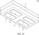
- the circuit layer 2 and the soldering pad 3 are respectively disposed on the first surface 11 and the second surface 12 of the substrate 1.
- the circuit layer 2 is electrically connected to the soldering pad 3 by using the conductive pillars (not shown) of the substrate 1.
- the soldering pad 3 includes two groups of electrode soldering pads 31, and the two groups of electrode soldering pads 31 are respectively and electrically connected to the light-emitting unit 5 and the auxiliary light-emitting unit 5' through the circuit layer 2 and the conductive pillars of the substrate 1.
- the circuit layer 2 includes two sets of the electrode pads 21, 22, 21', 22'.
- One set having the first electrode 21 and the second electrode 22 is provided for mounting the light-emitting unit 5, and the other set having the first electrode 21' and the second electrode 22' is provided for mounting the auxiliary light-emitting unit 5'.
- the first electrode 21 having an L shape includes a first bonding region 211 and a first extending region 212 extended from the first bonding region 211.
- the second electrode 22 having an L shape includes a second bonding region 221 and a second extending region 222 extended from the second bonding region 221.
- the first electrode 21' having an L shape includes a first bonding region 211' and a first extending region 212' extended from the first bonding region 211'.
- the two first extending regions 212, 212' are arranged adjacent to each other.
- the second electrode 22' has a straight shape, and the length of the second electrode 22' is equal to that of the first electrode 21'.
- first bonding region 211 of the first electrode 21 and the second bonding region 221 of the second electrode 22 are provided for the light-emitting unit 5 having a flip chip manner and the light-emitting unit 5 is mounted thereon.
- the first extending region 212, 212' of the first electrode 21, 21' are provided for the Zener diode chips 6 and the Zener diode chips 6 are mounted thereon.
- the Zener diode chips 6 are further electrically connected to the second extending region 222 of the second electrode 22 and the second electrode 22' by wire-bonding.
- the first bonding region 211' of the first electrode 21' is provided for the auxiliary light-emitting unit 5' and the auxiliary light-emitting unit 5' is mounted thereon.
- the auxiliary light-emitting unit 5' is electrically connected to the second electrode 22' by wire-bonding.
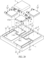
- FIGs. 27 through 29 show a fifth embodiment.
- the fifth embodiment is similar to the fourth embodiment, and the identical features are not disclosed again.
- the different features between the two embodiments are disclosed as follows.
- the auxiliary light-emitting unit 5' in the instant embodiment includes a red LED chip 52', a green LED chip 53', and a blue LED chip 54', and the other components (i.e., the substrate 1, the circuit layer 2, the soldering pad 3, the Zener diode chip 6, and the light transparent layer 9) are adjusted in size and number according to the auxiliary light-emitting unit 5'.
- the circuit layer 2 includes four first electrodes 21, 21' and four second electrodes 22, 22' respectively arranged adjacent to the four first electrodes 21, 21'. The four first electrodes 21, 21' are respectively cooperated with the four second electrodes 22, 22' to be classified into four sets.
- the light-emitting unit 5 is mounted on one of the four sets having the first electrode 21 and the second electrode 22, and the red LED chip 52', the green LED chip 53', and the blue LED chip 54' are respectively mounted on the other three sets each having the first electrode 21' and the second electrode 22'.
- a half part of the circuit layer 2 for the light-emitting unit 5 and the red LED chip 52' is substantially identical to the circuit layer 2 of the fourth embodiment, and the other half part of the circuit layer 2 for the green LED chip 53' and the blue LED chip 54' are a 2-fold rotational symmetry with respect to a central axis thereof.
- the first electrode 21' and the second electrode 22', which are corresponding to the red LED chip 52' are substantially mirror symmetrical to the first electrode 21' and the second electrode 22', which are corresponding to the blue LED chip 54'.
- the four Zener diode chips 6 are respectively mounted on the four first extending regions 212, 212' and are arranged in one row.
- the light transparent layer 9 includes a top plane 91 arranged away from the substrate 1 and an outer lateral surface 92 aligned with the side surface of the substrate 1.
- a distance between the top plane 91 of the light transparent layer 9 and the substrate 1 is equal to or less than a distance between the top plane 521 of the light-emitting unit 5 and the substrate 1.
- the top plane 91 of the light transparent layer 9 is substantially lower than or equal to that of the light-emitting unit 5.
- the two top planes 91, 521 are parallel to each other.
- the distance between the two top planes 91, 521 is zero, or in a range of 1 ⁇ 30 ⁇ m (i.e., in a range of 0 ⁇ 30 ⁇ m) and is preferably in a range of 15 ⁇ m ⁇ 30 ⁇ m. More specifically, the light transparent layer 9 has an opening to expose the top plane 521 of the light-emitting unit 5.
- the soldering pad 3 includes four groups of electrode soldering pads 31, and the four groups of electrode soldering pads 312 are respectively and electrically connected to the light-emitting unit 5, the red LED chip 52', the green LED chip 53', and the blue LED chip 54' through the circuit layer 2 and the conductive pillars of the substrate 1.
- the light-emitting unit of the LED package structure of the instant disclosure is disposed on the substrate, and the fluorescent body of the light-emitting unit is spaced apart from the substrate with a gap having a range of 3 ⁇ m ⁇ 10 ⁇ m.
- the gap is filled with the reflective housing (or the light transparent layer), such that electrical connection between the light-emitting unit and the circuit layer is not influenced by the fluorescent body, thereby the poor electrical connection can be improved.
- the top plane of the reflective housing is equal to that of the light-emitting unit, or the top plane of the reflective housing is lower than that of the light-emitting unit, and the distance between the two top planes is zero or in a range of 1 ⁇ 30 ⁇ m, and include the additional features as defined in the independent claims, thus problems about light shape and poor brightness can be avoided.
- each of the light-emitting units and the Zener diode chip can be mounted on the first electrode and the second electrode because of the layout of the circuit layer, thereby reducing the size of the circuit layer.
- the opening of the first notch and the opening of the second notch respectively face toward two sides away from each other in the width direction of the substrate, such that the patterned area of the circuit layer patterned on the first surface of the substrate is effectively decreased, thereby increasing the area of the insulating layer covering on the first surface of the substrate.
- a current leakage can be prevented through the insulating layer being arranged between the first electrode and the second electrode.
- the top surface and the side surface of the LED chip are encapsulated by the fluorescent body, such that the light leakage problem of the LED chip can be improved.
- the forward light efficiency of the LED package structure can be effectively increased and the yellow ring and blue ring can be avoided by forming the reflective housing and embedding the Zener diode chip in the reflective housing.
- the color uniformity of the LED package structure can be effectively increased by disposing the light diffusion layer.
- the substrate has a ESD function identical to the Zener diode chip, such that the Zener diode chip can be omitted to reduce the size of the LED package structure, and the light-emitting unit 5 can be arranged at an optical center of the LED package structure.
- the longitudinal direction of each electrode soldering pad is substantially perpendicular to that of each of the first electrode and the second electrode, such that a warpage problem, which is easily happened due to the components having different coefficients of thermal expansion (CTE), can be avoided during the manufacturing process of the LED package structure.
- the first electrodes and the second electrodes are provided in the specific arrangement to effectively decrease the occupied area of the first surface and to reduce the distance between the two light-emitting units, thereby increasing the light performance of the LED package structure.
- the LED package structure can be provided for the user with a plurality of operating modes through the two groups of electrode soldering pads to control the two light-emitting units.
- the insulating layer and the reflective housing of the third embodiment is replaced by the light transparent layer in the fourth and fifth embodiments and one of the light-emitting units of the third embodiment is replaced by the auxiliary light-emitting unit for different application of the LED package structure.
Landscapes
- Physics & Mathematics (AREA)
- General Physics & Mathematics (AREA)
- Optics & Photonics (AREA)
- Led Device Packages (AREA)
- Engineering & Computer Science (AREA)
- Microelectronics & Electronic Packaging (AREA)
- Power Engineering (AREA)
- Condensed Matter Physics & Semiconductors (AREA)
- Computer Hardware Design (AREA)
Claims (13)
- LED-Gehäuse-Struktur, welche aufweist:ein Substrat (1), welches eine erste Fläche (11) und eine zweite Fläche (12), welche entgegengesetzt zur ersten Fläche (11) ist, hat;eine Schaltungsschicht (2), welche auf der ersten Fläche (11) des Substrats (1) angeordnet ist;eine Isolierschicht (4), welche auf der ersten Fläche (11) des Substrats (1) angeordnet ist, wobei die Isolierschicht (4) und die Schaltungsschicht (2) koplanar sind und mit einer komplementären Form angeordnet sind;mindestens eine lichtemittierende Einheit (5), welche ein Chip Scale Package (CSP) ist und einen LED-Chip (51) und einen fluoreszierenden Körper (52) aufweist, welcher eine obere Fläche (512) und eine Seitenfläche (513) des LED-Chips (51) einkapselt, wobei der LED-Chip (51) auf der Schaltungsschicht (2) und der Isolierschicht (4) montiert ist, und der fluoreszierende Körper (52) von der Schaltungsschicht (2) mit einem Spalt (G) in einem Bereich von 3 µm bis 10 µm räumlich getrennt ist, wobei der fluoreszierende Körper (52) mindestens zwei Chipelektroden (511) des LED-Chips (51) freilegt und die obere Fläche (512) des LED-Chips (51) parallel zu einer oberen Fläche (521) des fluoreszierenden Körpers (52) ist;ein reflektierendes Gehäuse (7), welches auf der Schaltungsschicht (2) und der Isolierschicht (4) angeordnet ist, um die mindestens eine lichtemittierende Einheit (5) zu umgeben, und ferner in den Spalt (G) gefüllt ist, sodass das reflektierende Gehäuse (7) konfiguriert ist, um eine Seitenfläche der mindestens einen lichtemittierenden Einheit (5), eine Seitenfläche einer Chipelektrode (511) der mindestens einen lichtemittierenden Einheit (5) und eine Bodenfläche des fluoreszierenden Körpers (52) zu bedecken, wobei jedes vom reflektierenden Gehäuse (7) und der mindestens einen lichtemittierenden Einheit (5) eine obere Fläche (521), welche vom Substrat (1) entfernt angeordnet ist, hat, wobei die obere Fläche (71) des reflektierenden Gehäuses (7) im Wesentlichen niedriger als oder gleich zu derjenigen der mindestens einen lichtemittierenden Einheit (5) ist, und ein Abstand (D4) zwischen den beiden oberen Flächen (521, 71) Null oder in einem Bereich von 1 bis 30 µm ist; und wobei die lichtemittierende Einheit (5) eine reflektierende Schale (53) aufweist, welche auf der Seitenfläche (513) des fluoreszierenden Körpers (52) ausgebildet ist, undein Lötpad (3), welches auf der zweiten Fläche (12) des Substrats (1) angeordnet und elektrisch mit der Schaltungsschicht (2) verbunden ist.
- LED-Gehäuse-Struktur nach Anspruch 1, wobei die Schaltungsschicht (2) aufweist:eine erste Elektrode (21), welche einen ersten Bindungsbereich (211), einen ersten Erstreckungsbereich (212) und einen ersten Verbindungsbereich (213), welcher mit dem ersten Bindungsbereich (211) und dem ersten Erstreckungsbereich (212) verbunden ist, aufweist, wobei eine erste Nut (214) mittels des ersten Bindungsbereichs (211), des ersten Verbindungsbereichs (213) und des ersten Erstreckungsbereichs (212) definiert ist; undeine zweite Elektrode (22), welche einen zweiten Bindungsbereich (221), einen zweiten Erstreckungsbereich (222) und einen zweiten Verbindungsbereich (223), welcher mit den zweiten Bindungsbereich (221) und dem zweiten Erstreckungsbereich (222) verbunden ist, aufweist, wobei eine zweite Nut (224) mittels des zweiten Bindungsbereichs (221), des zweiten Verbindungsbereichs (223) und des zweiten Erstreckungsbereichs (222) definiert ist, wobei eine Öffnung der ersten Nut (214) und eine Öffnung der zweiten Nut (224) entsprechend zugeordnet in Richtung zweier voneinander entfernter Seiten blicken, und die erste Elektrode (21) und die zweite Elektrode (22) im Wesentlichen spiegelsymmetrisch angeordnet sind;wobei der LED-Chip (51) auf dem ersten Bindungsbereich (211) und dem zweiten Bindungsbereich (221) montiert ist, und ein Zener-Dioden-Chip (6) auf dem ersten Erstreckungsbereich (212) und dem zweiten Erstreckungsbereich (222) montiert ist.
- LED-Gehäuse-Struktur nach Anspruch 2, wobei ein Abstand (D1) zwischen dem ersten Bindungsbereich (211) und dem zweiten Bindungsbereich (221) größer als ein Abstand (D2) zwischen dem ersten Erstreckungsbereich (212) und dem zweiten Erstreckungsbereich (222) ist.
- LED-Gehäuse-Struktur nach Anspruch 1, wobei ein kleinster Abstand (D3) zwischen der oberen Fläche (512) des LED-Chips (51) und der oberen Fläche (521) des fluoreszierenden Körpers (52) in einem Bereich von 50 µm bis 200 µm ist.
- LED-Gehäuse-Struktur nach Anspruch 1, wobei die LED-Gehäuse-Struktur ferner eine Lichtdiffusionsschicht (8) aufweist, welche auf dem reflektierenden Gehäuse (7) und dem fluoreszierenden Körper (52) angeordnet ist, wobei eine Dicke der Lichtdiffusionsschicht (8) geringer als oder gleich 50 µm ist und die Lichtdiffusionsschicht (8) Siliziumdioxid oder Titandioxid mit einem Gewichtsprozentanteil von 2 Gew.-% bis 5 Gew.-% aufweist.
- LED-Gehäuse-Struktur nach Anspruch 1, wobei das Lötpad (3) zwei Elektroden-Lötpads (31) und ein wärmeableitendes Lötpad (32) aufweist, wobei die zwei Elektroden-Lötpads (31) elektrisch mit der Schaltungsschicht (2) verbunden sind, und die zwei Elektroden-Lötpads (31) elektrisch mit dem LED-Chip (51) durch die Schaltungsschicht (2) verbunden sind, das wärmeableitende Lötpad (32) auf einer Seite der zwei Elektroden-Lötpads (31) angeordnet ist und unter dem LED-Chip (51) ist, zum Ableiten von Wärme, welche von dem LED-Chip (51) erzeugt wird.
- LED-Gehäuse-Struktur nach Anspruch 1, wobei das Substrat (1) eine Keramikschicht (14), zumindest eine Varistorschicht (15), welche auf einer Seite der Keramikschicht (14) angeordnet ist, zwei erste leitfähige Säulen (131), welche in die Keramikschicht (14) eingebettet sind, und zwei zweite leitfähige Säulen (132), welche in die zumindest eine Varistorschicht (15) eingebettet sind, aufweist, wobei die zwei ersten leitfähigen Säulen (131) entsprechend zugeordnet elektrisch mit den zwei zweiten leitfähigen Säulen (132) verbunden sind, wobei die ersten leitfähigen Säulen (131) und die zweiten leitfähigen Säulen (132) elektrisch mit der Schaltungsschicht (2) und dem Lötpad (3) verbunden sind, und wobei die zumindest eine Varistorschicht (15) zumindest zwei metallische Schichten (151) aufweist, welche elektrisch mit den zwei zweiten leitfähigen Säulen (132) verbunden sind, um einen kapazitiven Effekt zu haben.
- LED-Gehäuse-Struktur nach Anspruch 1, wobei zumindest zwei lichtemittierende Einheiten (5), welche unterschiedliche Farbtemperatur haben, auf der Schaltungsschicht (2) und der Isolierschicht (4) angeordnet sind, und ein Abstand (D7) zwischen den zwei lichtemittierenden Einheiten (5) in einem Bereich von 0,3 mm bis 0,5 mm ist.
- LED-Gehäuse-Struktur nach Anspruch 8, wobei die LED-Gehäuse-Struktur weiter zwei Zener-Dioden-Chips (6) aufweist, wobei die Schaltungsschicht (2) aufweist:zwei erste Elektroden (21), wobei jede der zwei ersten Elektroden (21) eine L-förmige Konstruktion, welche einen ersten Bindungsbereich (211) und einem ersten Erstreckungsbereich (212), welcher senkrecht mit dem ersten Bindungsbereich (211) verbunden ist, hat; undzwei zweite Elektroden (22), welche an einer inneren Seite der zwei ersten Elektroden (21) angeordnet sind, wobei jede der zwei zweiten Elektroden (22) eine L-förmige Konstruktion aufweist, welche einen zweiten Bindungsbereich (221) und einen zweiten Erstreckungsbereich (222) hat, welcher senkrecht mit dem zweiten Bindungsbereich (221) verbunden ist;wobei die L-förmigen Konstruktionen der zwei ersten Elektroden (21) zwei Ecken in einer Position aufweisen, welche entsprechend zugeordnet zwei diagonalen Ecken des Substrats (1) entspricht, und die L-förmigen Konstruktionen der zwei zweiten Elektroden (22) zwei Ecken aufweisen, welche entsprechend zugeordnet an einer inneren Seite der zwei Ecken der zwei ersten Elektroden (21) angeordnet sind; wobei die ersten Bindungsbereiche (211) und die zweiten Bindungsbereiche (221) paarweise sind und konfiguriert sind, um mit den zwei lichtemittierenden Einheiten (5) verbunden zu sein, und die ersten Erstreckungsbereiche (212) und die zweiten Erstreckungsbereiche (222) paarweise sind und konfiguriert sind, um mit den Zener-Dioden-Chips (6) zu verbinden.
- LED-Gehäuse-Struktur nach Anspruch 9, wobei die Schaltungsschicht (2) eine 2-fache Rotationssymmetrie entlang einer zentralen Achse senkrecht zum Substrat (1) hat, ein Abstand (D1) zwischen jedem der ersten Bindungsbereiche (211) und der zweiten Bindungsbereiche (221) im Wesentlichen in einem Bereich von 90 µm bis 150 µm ist, und ein Abstand (D2) zwischen jedem der ersten Erstreckungsbereiche (212) und der zweiten Erstreckungsbereiche (222) im Wesentlichen in einem Bereich von 150 µm bis 200 µm ist.
- LED-Gehäuse-Struktur, welche aufweist:ein Substrat (1), welches eine erste Fläche (11) und eine zweite Fläche (12) hat, welche der ersten Fläche (11) entgegengesetzt ist;eine Schaltungsschicht (2), welche auf der ersten Fläche (11) des Substrats (1) angeordnet ist;mindestens eine lichtemittierende Einheit (5), welche ein Chip Scale Package (CSP) ist und einen LED-Chip (51) und einen fluoreszierenden Körper (52) aufweist, welcher eine obere Fläche (512) und Seitenflächen (513) des LED-Chips (51) einkapselt, wobei der LED-Chip (51) auf der Schaltungsschicht (2) montiert ist, der fluoreszierende Körper (52) von der Schaltungsschicht (2) räumlich getrennt ist, und der fluoreszierende Körper (52) von der Schaltungsschicht (2) mit einem Spalt (G), welcher einen Bereich von 3 µm bis 10 µm hat, räumlich getrennt ist, wobei der fluoreszierende Körper (52) mindestens zwei Chipelektroden (511) des LED-Chips (51) freilegt und die obere Fläche (512) des LED-Chips (51) parallel zu einer oberen Fläche (521) des fluoreszierenden Körpers (52) ist;zumindest eine zusätzliche lichtemittierende Einheit (5'), welche auf der Schaltungsschicht (2) montiert ist;eine lichtdurchlässige Schicht (9), welche auf dem Substrat (1) angeordnet ist, um die mindestens eine lichtemittierende Einheit (5) und die mindestens eine zusätzliche lichtemittierende Einheit (5') einzukapseln, sodass die lichtdurchlässige Schicht (9) konfiguriert ist, um eine Seitenfläche der lichtemittierenden Einheit (5) zu bedecken, eine Seitenfläche einer Chipelektrode (511) der zumindest einen lichtemittierenden Einheit (5), eine Bodenfläche (523) des fluoreszierenden Körpers (52), eine Seitenfläche der zumindest einen zusätzlichen lichtemittierenden Einheit (5') und einer Seitenfläche einer Chipelektrode der mindestens einen zusätzlichen lichtemittierenden Einheit (5'), wobei jede der lichtdurchlässige Schicht (9) und der lichtemittierende Einheit (5) eine obere Ebene (521) hat, welche entfernt vom Substrat (1) angeordnet ist, wobei die obere Ebene (91) der lichtdurchlässigen Schicht (9) im Wesentlichen niedriger als oder gleich derjenigen der lichtemittierenden Einheit (5) ist, und wobei ein Abstand zwischen den zwei oberen Ebenen (521, 91) Null oder in einem Bereich von 1 bis 30 µm ist; undein Lötpad (3), welches auf der zweiten Fläche (12) des Substrats (1) angeordnet ist und elektrisch mit der Schaltungsschicht (2) verbunden ist, wobei das Lötpad (3) mindestens zwei Gruppen von Elektroden-Löt-Pads (31) aufweist entsprechend zugeordnet und elektrisch mit der mindestens einen lichtemittierenden Einheit (5) und der mindestens einen zusätzlichen lichtemittierenden Einheit (5') verbunden ist.
- LED-Gehäuse-Struktur nach Anspruch 11, wobei die zusätzliche lichtemittierende Einheit (5') aus der Gruppe ausgewählt ist, welche aus einem UV-LED-Chip (51'), einem roten LED-Chip (52'), einem grünen LED-Chip (53') und einem blauen LED-Chip (54') besteht.
- LED-Gehäuse-Struktur gemäß Anspruch 11, wobei die lichtemittierende Einheit (5) eine reflektierende Schale (53) aufweist, welche eine Seitenfläche (513) des LED-Chips (51) umgibt.
Applications Claiming Priority (1)
| Application Number | Priority Date | Filing Date | Title |
|---|---|---|---|
| CN201610405811.9A CN107482099B (zh) | 2016-06-08 | 2016-06-08 | 发光二极管封装结构 |
Publications (2)
| Publication Number | Publication Date |
|---|---|
| EP3255686A1 EP3255686A1 (de) | 2017-12-13 |
| EP3255686B1 true EP3255686B1 (de) | 2023-03-08 |
Family
ID=57326296
Family Applications (1)
| Application Number | Title | Priority Date | Filing Date |
|---|---|---|---|
| EP16199084.1A Active EP3255686B1 (de) | 2016-06-08 | 2016-11-16 | Led-gehäusestruktur |
Country Status (4)
| Country | Link |
|---|---|
| US (1) | US9705052B1 (de) |
| EP (1) | EP3255686B1 (de) |
| JP (1) | JP6284659B2 (de) |
| CN (1) | CN107482099B (de) |
Families Citing this family (19)
| Publication number | Priority date | Publication date | Assignee | Title |
|---|---|---|---|---|
| EP4273944A3 (de) * | 2015-04-02 | 2024-02-07 | Nichia Corporation | Lichtemittierende vorrichtung und verfahren zur seiner herstellung |
| US10522728B2 (en) | 2017-01-26 | 2019-12-31 | Maven Optronics Co., Ltd. | Beveled chip reflector for chip-scale packaging light-emitting device and manufacturing method of the same |
| WO2019006763A1 (en) * | 2017-07-07 | 2019-01-10 | Cree Hong Kong Limited | RGB LED BOX WITH BSY TRANSMITTER |
| CN112331623B (zh) * | 2017-12-15 | 2024-09-20 | 光宝科技股份有限公司 | 发光二极管封装结构及散热基板 |
| JP7092506B2 (ja) * | 2018-01-09 | 2022-06-28 | スタンレー電気株式会社 | 発光装置 |
| JP2019201089A (ja) * | 2018-05-15 | 2019-11-21 | マブン オプトロニックス カンパニー リミテッドMaven Optronics Co., Ltd. | チップスケールパッケージング発光素子の斜角チップ反射器およびその製造方法 |
| DE102018111791A1 (de) * | 2018-05-16 | 2019-11-21 | Osram Opto Semiconductors Gmbh | Optoelektronisches Bauteil |
| US11264527B2 (en) * | 2018-10-01 | 2022-03-01 | Medtronic, Inc. | Integrated circuit package and system using same |
| CN111276596B (zh) * | 2018-12-05 | 2024-02-06 | 光宝光电(常州)有限公司 | 发光单元 |
| US11588074B2 (en) | 2019-02-01 | 2023-02-21 | Lite-On Opto Technology (Changzhou) Co., Ltd. | Light source device |
| US11217572B2 (en) | 2019-02-01 | 2022-01-04 | Lite-On Opto Technology (Changzhou) Co., Ltd. | Light source device |
| CN111520619A (zh) * | 2019-02-01 | 2020-08-11 | 光宝光电(常州)有限公司 | 光源装置 |
| CN110346855B (zh) * | 2019-07-31 | 2021-08-31 | 浙江舜宇光学有限公司 | 光扩散片的制备方法 |
| USD993199S1 (en) * | 2020-06-22 | 2023-07-25 | Epistar Corporation | Light-emitting device |
| US12009459B2 (en) * | 2020-08-14 | 2024-06-11 | Lite-On Technology Corporation | Light-emitting device, light-emitting assembly, and integrated circuit flip-chip |
| CN214956944U (zh) * | 2020-08-14 | 2021-11-30 | 光宝科技股份有限公司 | 发光封装模组 |
| KR20230121077A (ko) * | 2020-12-18 | 2023-08-17 | 서울바이오시스 주식회사 | 발광 다이오드 패키지 |
| KR20220102508A (ko) | 2021-01-13 | 2022-07-20 | 삼성전자주식회사 | LED(Light Emitting Diode) 패키지 및 이를 포함하는 조명 장치 |
| TWI787999B (zh) * | 2021-09-09 | 2022-12-21 | 同欣電子工業股份有限公司 | 感測器封裝結構及其製造方法 |
Citations (1)
| Publication number | Priority date | Publication date | Assignee | Title |
|---|---|---|---|---|
| US20150311405A1 (en) * | 2012-12-10 | 2015-10-29 | Citizen Holding Co., Ltd. | Led device and manufacturing method thereof |
Family Cites Families (14)
| Publication number | Priority date | Publication date | Assignee | Title |
|---|---|---|---|---|
| KR100896068B1 (ko) * | 2007-11-30 | 2009-05-07 | 일진반도체 주식회사 | 정전기 방전 보호 기능을 갖는 발광다이오드 소자 |
| US8384114B2 (en) * | 2009-06-27 | 2013-02-26 | Cooledge Lighting Inc. | High efficiency LEDs and LED lamps |
| US8803201B2 (en) * | 2011-01-31 | 2014-08-12 | Cree, Inc. | Solid state lighting component package with reflective layer |
| JP2012138454A (ja) * | 2010-12-27 | 2012-07-19 | Citizen Holdings Co Ltd | 半導体発光装置及びその製造方法 |
| US9269878B2 (en) * | 2011-05-27 | 2016-02-23 | Lg Innotek Co., Ltd. | Light emitting device and light emitting apparatus |
| US9153758B2 (en) * | 2011-06-01 | 2015-10-06 | Koninklijke Philips N.V. | Method of attaching a light emitting device to a support substrate |
| CN103199172B (zh) * | 2012-01-10 | 2015-10-07 | 展晶科技(深圳)有限公司 | 发光二极管封装结构的制造方法 |
| US8783911B2 (en) * | 2012-02-17 | 2014-07-22 | Tsmc Solid State Lighting Ltd. | LED packaging structure having improved thermal dissipation and mechanical strength |
| DE102012102847A1 (de) * | 2012-04-02 | 2013-10-02 | Osram Opto Semiconductors Gmbh | Licht emittierendes Halbleiterbauelement und Verfahren zur Herstellung eines Licht emittierenden Halbleiterbauelements |
| JP2015207754A (ja) * | 2013-12-13 | 2015-11-19 | 日亜化学工業株式会社 | 発光装置 |
| CN104716246B (zh) * | 2013-12-17 | 2017-09-26 | 展晶科技(深圳)有限公司 | 光电元件封装结构及其制造方法 |
| EP3547379A1 (de) * | 2014-03-14 | 2019-10-02 | Citizen Electronics Co., Ltd. | Lichtemittierende vorrichtung |
| DE102014112883A1 (de) * | 2014-09-08 | 2016-03-10 | Osram Opto Semiconductors Gmbh | Optoelektronisches Bauteil |
| WO2016123065A1 (en) * | 2015-01-26 | 2016-08-04 | Cooledge Lighting, Inc. | Systems and methods for adhesive bonding of electronic devices |
-
2016
- 2016-06-08 CN CN201610405811.9A patent/CN107482099B/zh active Active
- 2016-10-28 US US15/338,289 patent/US9705052B1/en active Active
- 2016-11-16 EP EP16199084.1A patent/EP3255686B1/de active Active
-
2017
- 2017-01-16 JP JP2017005373A patent/JP6284659B2/ja active Active
Patent Citations (1)
| Publication number | Priority date | Publication date | Assignee | Title |
|---|---|---|---|---|
| US20150311405A1 (en) * | 2012-12-10 | 2015-10-29 | Citizen Holding Co., Ltd. | Led device and manufacturing method thereof |
Also Published As
| Publication number | Publication date |
|---|---|
| US9705052B1 (en) | 2017-07-11 |
| JP2017220661A (ja) | 2017-12-14 |
| CN107482099A (zh) | 2017-12-15 |
| CN107482099B (zh) | 2019-09-10 |
| EP3255686A1 (de) | 2017-12-13 |
| JP6284659B2 (ja) | 2018-02-28 |
Similar Documents
| Publication | Publication Date | Title |
|---|---|---|
| EP3255686B1 (de) | Led-gehäusestruktur | |
| US9786827B2 (en) | Light emitting diode package | |
| US7768754B2 (en) | Ceramic substrate for light emitting diode where the substrate incorporates ESD protection | |
| CN204391155U (zh) | Led模块 | |
| US9842973B2 (en) | Method of manufacturing ceramic LED packages with higher heat dissipation | |
| US7808013B2 (en) | Integrated heat spreaders for light emitting devices (LEDs) and related assemblies | |
| US10234100B2 (en) | Optical lens, light emitting device, and light emitting module having same | |
| US8748200B2 (en) | Method for manufacturing LED package | |
| KR20090002319A (ko) | 발광 다이오드 패키지 및 그 제조방법 | |
| CN102549785B (zh) | 发光装置 | |
| CN109075230B (zh) | 发光装置 | |
| CN102479910A (zh) | Led模块 | |
| TW201327948A (zh) | 發光二極體封裝與製作方法 | |
| TWI572067B (zh) | 發光二極體封裝結構 | |
| WO2019112345A1 (ko) | 발광소자 패키지 및 광원 장치 | |
| US20180331084A1 (en) | Light emitting device and method of manufacturing the light emitting device | |
| CN104904025B (zh) | 发光装置的制造方法和发光装置 | |
| JP2007335734A (ja) | 半導体装置 | |
| US20250301834A1 (en) | Semiconductor light emitting apparatus | |
| TW201606229A (zh) | 具有led的led模組 |
Legal Events
| Date | Code | Title | Description |
|---|---|---|---|
| PUAI | Public reference made under article 153(3) epc to a published international application that has entered the european phase |
Free format text: ORIGINAL CODE: 0009012 |
|
| STAA | Information on the status of an ep patent application or granted ep patent |
Free format text: STATUS: THE APPLICATION HAS BEEN PUBLISHED |
|
| AK | Designated contracting states |
Kind code of ref document: A1 Designated state(s): AL AT BE BG CH CY CZ DE DK EE ES FI FR GB GR HR HU IE IS IT LI LT LU LV MC MK MT NL NO PL PT RO RS SE SI SK SM TR |
|
| AX | Request for extension of the european patent |
Extension state: BA ME |
|
| STAA | Information on the status of an ep patent application or granted ep patent |
Free format text: STATUS: REQUEST FOR EXAMINATION WAS MADE |
|
| 17P | Request for examination filed |
Effective date: 20180604 |
|
| RBV | Designated contracting states (corrected) |
Designated state(s): AL AT BE BG CH CY CZ DE DK EE ES FI FR GB GR HR HU IE IS IT LI LT LU LV MC MK MT NL NO PL PT RO RS SE SI SK SM TR |
|
| STAA | Information on the status of an ep patent application or granted ep patent |
Free format text: STATUS: EXAMINATION IS IN PROGRESS |
|
| 17Q | First examination report despatched |
Effective date: 20191218 |
|
| RIC1 | Information provided on ipc code assigned before grant |
Ipc: H01L 33/64 20100101ALN20220616BHEP Ipc: H01L 25/075 20060101ALI20220616BHEP Ipc: H01L 33/46 20100101ALI20220616BHEP Ipc: H01L 33/62 20100101ALI20220616BHEP Ipc: H01L 33/60 20100101ALI20220616BHEP Ipc: H01L 33/50 20100101ALI20220616BHEP Ipc: H01L 33/48 20100101AFI20220616BHEP |
|
| GRAP | Despatch of communication of intention to grant a patent |
Free format text: ORIGINAL CODE: EPIDOSNIGR1 |
|
| STAA | Information on the status of an ep patent application or granted ep patent |
Free format text: STATUS: GRANT OF PATENT IS INTENDED |
|
| INTG | Intention to grant announced |
Effective date: 20220922 |
|
| GRAS | Grant fee paid |
Free format text: ORIGINAL CODE: EPIDOSNIGR3 |
|
| GRAA | (expected) grant |
Free format text: ORIGINAL CODE: 0009210 |
|
| STAA | Information on the status of an ep patent application or granted ep patent |
Free format text: STATUS: THE PATENT HAS BEEN GRANTED |
|
| AK | Designated contracting states |
Kind code of ref document: B1 Designated state(s): AL AT BE BG CH CY CZ DE DK EE ES FI FR GB GR HR HU IE IS IT LI LT LU LV MC MK MT NL NO PL PT RO RS SE SI SK SM TR |
|
| REG | Reference to a national code |
Ref country code: GB Ref legal event code: FG4D |
|
| REG | Reference to a national code |
Ref country code: CH Ref legal event code: EP Ref country code: AT Ref legal event code: REF Ref document number: 1553177 Country of ref document: AT Kind code of ref document: T Effective date: 20230315 |
|
| REG | Reference to a national code |
Ref country code: DE Ref legal event code: R096 Ref document number: 602016078168 Country of ref document: DE |
|
| REG | Reference to a national code |
Ref country code: IE Ref legal event code: FG4D |
|
| REG | Reference to a national code |
Ref country code: LT Ref legal event code: MG9D |
|
| REG | Reference to a national code |
Ref country code: NL Ref legal event code: MP Effective date: 20230308 |
|
| PG25 | Lapsed in a contracting state [announced via postgrant information from national office to epo] |
Ref country code: RS Free format text: LAPSE BECAUSE OF FAILURE TO SUBMIT A TRANSLATION OF THE DESCRIPTION OR TO PAY THE FEE WITHIN THE PRESCRIBED TIME-LIMIT Effective date: 20230308 Ref country code: NO Free format text: LAPSE BECAUSE OF FAILURE TO SUBMIT A TRANSLATION OF THE DESCRIPTION OR TO PAY THE FEE WITHIN THE PRESCRIBED TIME-LIMIT Effective date: 20230608 Ref country code: LV Free format text: LAPSE BECAUSE OF FAILURE TO SUBMIT A TRANSLATION OF THE DESCRIPTION OR TO PAY THE FEE WITHIN THE PRESCRIBED TIME-LIMIT Effective date: 20230308 Ref country code: LT Free format text: LAPSE BECAUSE OF FAILURE TO SUBMIT A TRANSLATION OF THE DESCRIPTION OR TO PAY THE FEE WITHIN THE PRESCRIBED TIME-LIMIT Effective date: 20230308 Ref country code: HR Free format text: LAPSE BECAUSE OF FAILURE TO SUBMIT A TRANSLATION OF THE DESCRIPTION OR TO PAY THE FEE WITHIN THE PRESCRIBED TIME-LIMIT Effective date: 20230308 Ref country code: ES Free format text: LAPSE BECAUSE OF FAILURE TO SUBMIT A TRANSLATION OF THE DESCRIPTION OR TO PAY THE FEE WITHIN THE PRESCRIBED TIME-LIMIT Effective date: 20230308 |
|
| REG | Reference to a national code |
Ref country code: AT Ref legal event code: MK05 Ref document number: 1553177 Country of ref document: AT Kind code of ref document: T Effective date: 20230308 |
|
| PG25 | Lapsed in a contracting state [announced via postgrant information from national office to epo] |
Ref country code: SE Free format text: LAPSE BECAUSE OF FAILURE TO SUBMIT A TRANSLATION OF THE DESCRIPTION OR TO PAY THE FEE WITHIN THE PRESCRIBED TIME-LIMIT Effective date: 20230308 Ref country code: NL Free format text: LAPSE BECAUSE OF FAILURE TO SUBMIT A TRANSLATION OF THE DESCRIPTION OR TO PAY THE FEE WITHIN THE PRESCRIBED TIME-LIMIT Effective date: 20230308 Ref country code: GR Free format text: LAPSE BECAUSE OF FAILURE TO SUBMIT A TRANSLATION OF THE DESCRIPTION OR TO PAY THE FEE WITHIN THE PRESCRIBED TIME-LIMIT Effective date: 20230609 Ref country code: FI Free format text: LAPSE BECAUSE OF FAILURE TO SUBMIT A TRANSLATION OF THE DESCRIPTION OR TO PAY THE FEE WITHIN THE PRESCRIBED TIME-LIMIT Effective date: 20230308 |
|
| PG25 | Lapsed in a contracting state [announced via postgrant information from national office to epo] |
Ref country code: SM Free format text: LAPSE BECAUSE OF FAILURE TO SUBMIT A TRANSLATION OF THE DESCRIPTION OR TO PAY THE FEE WITHIN THE PRESCRIBED TIME-LIMIT Effective date: 20230308 Ref country code: RO Free format text: LAPSE BECAUSE OF FAILURE TO SUBMIT A TRANSLATION OF THE DESCRIPTION OR TO PAY THE FEE WITHIN THE PRESCRIBED TIME-LIMIT Effective date: 20230308 Ref country code: PT Free format text: LAPSE BECAUSE OF FAILURE TO SUBMIT A TRANSLATION OF THE DESCRIPTION OR TO PAY THE FEE WITHIN THE PRESCRIBED TIME-LIMIT Effective date: 20230710 Ref country code: EE Free format text: LAPSE BECAUSE OF FAILURE TO SUBMIT A TRANSLATION OF THE DESCRIPTION OR TO PAY THE FEE WITHIN THE PRESCRIBED TIME-LIMIT Effective date: 20230308 Ref country code: CZ Free format text: LAPSE BECAUSE OF FAILURE TO SUBMIT A TRANSLATION OF THE DESCRIPTION OR TO PAY THE FEE WITHIN THE PRESCRIBED TIME-LIMIT Effective date: 20230308 Ref country code: AT Free format text: LAPSE BECAUSE OF FAILURE TO SUBMIT A TRANSLATION OF THE DESCRIPTION OR TO PAY THE FEE WITHIN THE PRESCRIBED TIME-LIMIT Effective date: 20230308 |
|
| PG25 | Lapsed in a contracting state [announced via postgrant information from national office to epo] |
Ref country code: SK Free format text: LAPSE BECAUSE OF FAILURE TO SUBMIT A TRANSLATION OF THE DESCRIPTION OR TO PAY THE FEE WITHIN THE PRESCRIBED TIME-LIMIT Effective date: 20230308 Ref country code: PL Free format text: LAPSE BECAUSE OF FAILURE TO SUBMIT A TRANSLATION OF THE DESCRIPTION OR TO PAY THE FEE WITHIN THE PRESCRIBED TIME-LIMIT Effective date: 20230308 Ref country code: IS Free format text: LAPSE BECAUSE OF FAILURE TO SUBMIT A TRANSLATION OF THE DESCRIPTION OR TO PAY THE FEE WITHIN THE PRESCRIBED TIME-LIMIT Effective date: 20230708 |
|
| REG | Reference to a national code |
Ref country code: DE Ref legal event code: R097 Ref document number: 602016078168 Country of ref document: DE |
|
| PLBE | No opposition filed within time limit |
Free format text: ORIGINAL CODE: 0009261 |
|
| STAA | Information on the status of an ep patent application or granted ep patent |
Free format text: STATUS: NO OPPOSITION FILED WITHIN TIME LIMIT |
|
| PG25 | Lapsed in a contracting state [announced via postgrant information from national office to epo] |
Ref country code: SI Free format text: LAPSE BECAUSE OF FAILURE TO SUBMIT A TRANSLATION OF THE DESCRIPTION OR TO PAY THE FEE WITHIN THE PRESCRIBED TIME-LIMIT Effective date: 20230308 Ref country code: DK Free format text: LAPSE BECAUSE OF FAILURE TO SUBMIT A TRANSLATION OF THE DESCRIPTION OR TO PAY THE FEE WITHIN THE PRESCRIBED TIME-LIMIT Effective date: 20230308 |
|
| 26N | No opposition filed |
Effective date: 20231211 |
|
| PG25 | Lapsed in a contracting state [announced via postgrant information from national office to epo] |
Ref country code: IT Free format text: LAPSE BECAUSE OF FAILURE TO SUBMIT A TRANSLATION OF THE DESCRIPTION OR TO PAY THE FEE WITHIN THE PRESCRIBED TIME-LIMIT Effective date: 20230308 |
|
| REG | Reference to a national code |
Ref country code: CH Ref legal event code: PL |
|
| PG25 | Lapsed in a contracting state [announced via postgrant information from national office to epo] |
Ref country code: MC Free format text: LAPSE BECAUSE OF FAILURE TO SUBMIT A TRANSLATION OF THE DESCRIPTION OR TO PAY THE FEE WITHIN THE PRESCRIBED TIME-LIMIT Effective date: 20230308 |
|
| PG25 | Lapsed in a contracting state [announced via postgrant information from national office to epo] |
Ref country code: LU Free format text: LAPSE BECAUSE OF NON-PAYMENT OF DUE FEES Effective date: 20231116 |
|
| PG25 | Lapsed in a contracting state [announced via postgrant information from national office to epo] |
Ref country code: CH Free format text: LAPSE BECAUSE OF NON-PAYMENT OF DUE FEES Effective date: 20231130 |
|
| PG25 | Lapsed in a contracting state [announced via postgrant information from national office to epo] |
Ref country code: MC Free format text: LAPSE BECAUSE OF FAILURE TO SUBMIT A TRANSLATION OF THE DESCRIPTION OR TO PAY THE FEE WITHIN THE PRESCRIBED TIME-LIMIT Effective date: 20230308 Ref country code: LU Free format text: LAPSE BECAUSE OF NON-PAYMENT OF DUE FEES Effective date: 20231116 Ref country code: CH Free format text: LAPSE BECAUSE OF NON-PAYMENT OF DUE FEES Effective date: 20231130 |
|
| REG | Reference to a national code |
Ref country code: BE Ref legal event code: MM Effective date: 20231130 |
|
| REG | Reference to a national code |
Ref country code: IE Ref legal event code: MM4A |
|
| PG25 | Lapsed in a contracting state [announced via postgrant information from national office to epo] |
Ref country code: IE Free format text: LAPSE BECAUSE OF NON-PAYMENT OF DUE FEES Effective date: 20231116 |
|
| PG25 | Lapsed in a contracting state [announced via postgrant information from national office to epo] |
Ref country code: BE Free format text: LAPSE BECAUSE OF NON-PAYMENT OF DUE FEES Effective date: 20231130 |
|
| PG25 | Lapsed in a contracting state [announced via postgrant information from national office to epo] |
Ref country code: IE Free format text: LAPSE BECAUSE OF NON-PAYMENT OF DUE FEES Effective date: 20231116 Ref country code: BE Free format text: LAPSE BECAUSE OF NON-PAYMENT OF DUE FEES Effective date: 20231130 |
|
| PG25 | Lapsed in a contracting state [announced via postgrant information from national office to epo] |
Ref country code: BG Free format text: LAPSE BECAUSE OF FAILURE TO SUBMIT A TRANSLATION OF THE DESCRIPTION OR TO PAY THE FEE WITHIN THE PRESCRIBED TIME-LIMIT Effective date: 20230308 |
|
| REG | Reference to a national code |
Ref country code: DE Ref legal event code: R079 Ref document number: 602016078168 Country of ref document: DE Free format text: PREVIOUS MAIN CLASS: H01L0033480000 Ipc: H10H0020850000 |
|
| PG25 | Lapsed in a contracting state [announced via postgrant information from national office to epo] |
Ref country code: BG Free format text: LAPSE BECAUSE OF FAILURE TO SUBMIT A TRANSLATION OF THE DESCRIPTION OR TO PAY THE FEE WITHIN THE PRESCRIBED TIME-LIMIT Effective date: 20230308 |
|
| PG25 | Lapsed in a contracting state [announced via postgrant information from national office to epo] |
Ref country code: CY Free format text: LAPSE BECAUSE OF FAILURE TO SUBMIT A TRANSLATION OF THE DESCRIPTION OR TO PAY THE FEE WITHIN THE PRESCRIBED TIME-LIMIT; INVALID AB INITIO Effective date: 20161116 |
|
| PG25 | Lapsed in a contracting state [announced via postgrant information from national office to epo] |
Ref country code: HU Free format text: LAPSE BECAUSE OF FAILURE TO SUBMIT A TRANSLATION OF THE DESCRIPTION OR TO PAY THE FEE WITHIN THE PRESCRIBED TIME-LIMIT; INVALID AB INITIO Effective date: 20161116 |
|
| PG25 | Lapsed in a contracting state [announced via postgrant information from national office to epo] |
Ref country code: TR Free format text: LAPSE BECAUSE OF FAILURE TO SUBMIT A TRANSLATION OF THE DESCRIPTION OR TO PAY THE FEE WITHIN THE PRESCRIBED TIME-LIMIT Effective date: 20230308 |
|
| PGFP | Annual fee paid to national office [announced via postgrant information from national office to epo] |
Ref country code: DE Payment date: 20251126 Year of fee payment: 10 |
|
| PGFP | Annual fee paid to national office [announced via postgrant information from national office to epo] |
Ref country code: GB Payment date: 20251125 Year of fee payment: 10 |
|
| PGFP | Annual fee paid to national office [announced via postgrant information from national office to epo] |
Ref country code: FR Payment date: 20251124 Year of fee payment: 10 |