EP0245934A2 - Low pressure chemical vapor deposition of metal silicide - Google Patents
Low pressure chemical vapor deposition of metal silicide Download PDFInfo
- Publication number
- EP0245934A2 EP0245934A2 EP87302693A EP87302693A EP0245934A2 EP 0245934 A2 EP0245934 A2 EP 0245934A2 EP 87302693 A EP87302693 A EP 87302693A EP 87302693 A EP87302693 A EP 87302693A EP 0245934 A2 EP0245934 A2 EP 0245934A2
- Authority
- EP
- European Patent Office
- Prior art keywords
- temperature
- substrate
- metal
- deposition
- mof6
- Prior art date
- Legal status (The legal status is an assumption and is not a legal conclusion. Google has not performed a legal analysis and makes no representation as to the accuracy of the status listed.)
- Withdrawn
Links
Images
Classifications
-
- C—CHEMISTRY; METALLURGY
- C23—COATING METALLIC MATERIAL; COATING MATERIAL WITH METALLIC MATERIAL; CHEMICAL SURFACE TREATMENT; DIFFUSION TREATMENT OF METALLIC MATERIAL; COATING BY VACUUM EVAPORATION, BY SPUTTERING, BY ION IMPLANTATION OR BY CHEMICAL VAPOUR DEPOSITION, IN GENERAL; INHIBITING CORROSION OF METALLIC MATERIAL OR INCRUSTATION IN GENERAL
- C23C—COATING METALLIC MATERIAL; COATING MATERIAL WITH METALLIC MATERIAL; SURFACE TREATMENT OF METALLIC MATERIAL BY DIFFUSION INTO THE SURFACE, BY CHEMICAL CONVERSION OR SUBSTITUTION; COATING BY VACUUM EVAPORATION, BY SPUTTERING, BY ION IMPLANTATION OR BY CHEMICAL VAPOUR DEPOSITION, IN GENERAL
- C23C16/00—Chemical coating by decomposition of gaseous compounds, without leaving reaction products of surface material in the coating, i.e. chemical vapour deposition [CVD] processes
- C23C16/22—Chemical coating by decomposition of gaseous compounds, without leaving reaction products of surface material in the coating, i.e. chemical vapour deposition [CVD] processes characterised by the deposition of inorganic material, other than metallic material
- C23C16/30—Deposition of compounds, mixtures or solid solutions, e.g. borides, carbides, nitrides
- C23C16/42—Silicides
-
- H—ELECTRICITY
- H10—SEMICONDUCTOR DEVICES; ELECTRIC SOLID-STATE DEVICES NOT OTHERWISE PROVIDED FOR
- H10D—INORGANIC ELECTRIC SEMICONDUCTOR DEVICES
- H10D64/00—Electrodes of devices having potential barriers
- H10D64/01—Manufacture or treatment
- H10D64/011—Manufacture or treatment of electrodes ohmically coupled to a semiconductor
- H10D64/0111—Manufacture or treatment of electrodes ohmically coupled to a semiconductor to Group IV semiconductors
- H10D64/0112—Manufacture or treatment of electrodes ohmically coupled to a semiconductor to Group IV semiconductors using conductive layers comprising silicides
-
- H—ELECTRICITY
- H10—SEMICONDUCTOR DEVICES; ELECTRIC SOLID-STATE DEVICES NOT OTHERWISE PROVIDED FOR
- H10D—INORGANIC ELECTRIC SEMICONDUCTOR DEVICES
- H10D64/00—Electrodes of devices having potential barriers
- H10D64/01—Manufacture or treatment
- H10D64/013—Manufacture or treatment of electrodes having a conductor capacitively coupled to a semiconductor by an insulator
- H10D64/01302—Manufacture or treatment of electrodes having a conductor capacitively coupled to a semiconductor by an insulator the insulator being formed after the semiconductor body, the semiconductor being silicon
- H10D64/01304—Manufacture or treatment of electrodes having a conductor capacitively coupled to a semiconductor by an insulator the insulator being formed after the semiconductor body, the semiconductor being silicon characterised by the conductor
- H10D64/01306—Manufacture or treatment of electrodes having a conductor capacitively coupled to a semiconductor by an insulator the insulator being formed after the semiconductor body, the semiconductor being silicon characterised by the conductor the conductor comprising a layer of silicon contacting the insulator, e.g. polysilicon
- H10D64/01308—Manufacture or treatment of electrodes having a conductor capacitively coupled to a semiconductor by an insulator the insulator being formed after the semiconductor body, the semiconductor being silicon characterised by the conductor the conductor comprising a layer of silicon contacting the insulator, e.g. polysilicon the conductor further comprising a non-elemental silicon additional conductive layer, e.g. a metal silicide layer formed by the reaction of silicon with an implanted metal
- H10D64/01312—Manufacture or treatment of electrodes having a conductor capacitively coupled to a semiconductor by an insulator the insulator being formed after the semiconductor body, the semiconductor being silicon characterised by the conductor the conductor comprising a layer of silicon contacting the insulator, e.g. polysilicon the conductor further comprising a non-elemental silicon additional conductive layer, e.g. a metal silicide layer formed by the reaction of silicon with an implanted metal the additional layer comprising a metal or metal silicide formed by deposition, i.e. without a silicidation reaction, e.g. sputter deposition
-
- H—ELECTRICITY
- H10—SEMICONDUCTOR DEVICES; ELECTRIC SOLID-STATE DEVICES NOT OTHERWISE PROVIDED FOR
- H10P—GENERIC PROCESSES OR APPARATUS FOR THE MANUFACTURE OR TREATMENT OF DEVICES COVERED BY CLASS H10
- H10P14/00—Formation of materials, e.g. in the shape of layers or pillars
- H10P14/40—Formation of materials, e.g. in the shape of layers or pillars of conductive or resistive materials
- H10P14/42—Formation of materials, e.g. in the shape of layers or pillars of conductive or resistive materials using a gas or vapour
- H10P14/43—Chemical deposition, e.g. chemical vapour deposition [CVD]
Definitions
- the present invention relates to a process for the low pressure chemical vapor deposition (LPCVD) of metal silicide, especially molybdenum silicide, on a substrate at a low temperature.
- LPCVD low pressure chemical vapor deposition
- MOS metal oxide semiconductor
- a layer combination exhibiting a lower resistance for example, one composed of a 300 nm thick doped polysilicon layer and a 200 nm thick metal disilicide layer wherein the metal is molybdenum, tungsten or tantalum.
- Metal silicides have attracted increasing attention recently as possible interconnect material for semiconductor integrated circuits.
- bilayer composite films of metal silicide and polycrystalline silicon have been found to provide low resistance gate and interconnect layers for MOS circuits and to be otherwise compatible with current silicon gate technology.
- polycide structures Such structures are commonly termed “polycide” structures.
- the sheet resistance of polycide structures is generally an order of magnitude lower than that of a single layer structure of doped polycrystalline silicon alone.
- Polycide structures are utilized to achieve a high conductivity, gate-level metallization for MOS devices. More particularly, polycide structures are utilized as gate material and interconnects in structures such as very high speed integrated circuits (VHSIC).
- VHSIC very high speed integrated circuits
- Polycide structures have been used, for example, as the gate material in insulated gate field effect transistor (IGFET) devices and other similar structures.
- IGFET insulated gate field effect transistor
- Polycide structures are conventionally produced by depositing undoped polycrystalline silicon by LPCVD, doping the polycrystalline silicon, e.g., by diffusion using phosphorus oxychloride, and then depositing the refractory metal silicide, e.g., tantalum silicide, thereover by co-sputtering from separate targets of metal and silicon. Subsequent annealing is required to obtain the desired low conductivity of the silicide layer.
- LPCVD LPCVD
- doping the polycrystalline silicon e.g., by diffusion using phosphorus oxychloride
- the refractory metal silicide e.g., tantalum silicide
- Tungsten disilicide has received particular attention as a candidate for such applications because its electrical resistivity is among the lowest of the metal silicides.
- tungsten disilicide grows a passivating silicon oxide layer if a silicon source is available and it is not attacked by HF solutions.
- Films of tungsten disilicide have been formed by sintering films of tungsten metal deposited on silicon by evaporation, sputtering or chemical vapor deposition (CVD). They have also been formed by sintering mixed films of tungsten and silicon formed by co-evaporation, co-sputtering, or sputtering from a tungsten disilicide target.
- U.S. Patent 4,359,490 describes a LPCVD process for co-depositing a metal, such as tungsten, molybdenum, tantalum and niobium, and silicon onto a surface such as a semiconductor integrated circuit.
- a LPCVD reactor is maintained at 500°-700°C and at a pressure of 0.1-0.3 torr.
- Conventional CVD purging steps are utilized and silane is introduced into the reactor to deposit a base layer of polysilicon on the desired surface.
- tantalum chloride for example, is introduced and a tantalum silicide layer is deposited on the surface at a rate of 100-300 angstroms/min.
- Molybdenum disilicide films have also been deposited by LPCVD. See, for example, Inoue et al., J.Electrochem.Soc. 130 , 1603 (1983). This process utilizes a hot wall procedure at 670°C.
- the LPCVD of tungsten silicide has also been described by Brors et al., Solid State Technol. , April 1983, p. 183; Saraswat et al., IEEE Trans.Elect.Dev. ED-30 , 1497 (1983) and Brors et al. Proc. Electrochem.Soc. 1984, Chem. Vap. Depos., p. 275-286.
- the depositions described by the Brors et al. references were conducted at 350°-450°C in a cold wall procedure.
- the LPCVD technique is currently preferred because it offers superior step coverage (over the sputtering technique), which is essential for state-of-the-art sub-micron devices.
- U.S. Patent 4,504,521 describes a similar process, but first deposits a doped amphorous silicon layer before depositing the tantalum silicide layer. According to this patent, a smooth surface of TaSi2 is deposited after annealing, which is not the case in U.S. Patent 4,359,490.
- a film of titanium silicide which is substantially titanium disilicide is deposited by chemical vapor deposition by reacting a gaseous silicon species and a gaseous titanium species in a plasma.
- the preferred reactant species are silane (SiH4) and titanium tetrachloride (TiCl4) which are carried into a reaction chamber by an inert gaseous carrier such as argon. Since SiH4 and TiCl4 decompose at different temperatures, thermal decomposition is inadequate to produce films of uniform composition and thickness over an extended reaction zone.
- the decomposition reaction takes place in a plasma at relatively low temperature (450°C) by alternating electrical field, by a process generally termed plasma-enhanced chemical vapor deposition (PECVD). After deposition, the material is annealed at 600°-700°C.
- PECVD plasma-enhanced chemical vapor deposition
- the present invention provides a low pressure chemical vapor deposition of a metal silicide at temperatures which are generally at least 100°C below temperatures currently being used.
- the walls of a LPCVD reactor which contains a heated pedestal for holding a substrate are cooled, and the pedestal is heated so the substrate temperature reaches a desired level, depending on the metal silicide to be deposited.
- a metal halide and silane or disilane are fed separately into the deposition chamber and mixed behind a small baffle plate at the entrance.
- the metal silicide is deposited on the substrate surface. It is preferred that the substrate be pre-treated with H2 plasma before deposition.
- the substrate receiving the metal silicide layer may be any material conventionally used in the electronics industry.
- a preferred substrate is a single crystal silicon wafer.
- the substrate may be partially processed, e.g., doped, to provide regions of conductivity.
- the substrate may have its oxide layer stripped away prior to metal silicide deposition or may still have its oxide layer.
- the substrate is placed in a conventional LPCVD reactor.
- the reactor contains a pedestal on which the substrate is placed.
- the pedestal is heated to the desired temperature, depending on the metal compound and silicon compound being used to form the metal silicide layer.
- the walls of the reactor are cooled either by simply blowing air on the outside walls of the reactor or actively cooling the reactor, such as through the use of a water jacket.
- active cooling or simple air cooling is dependent upon the temperature at which the deposition is to occur for the chosen reactants.
- a lower wall temperature is desired to avoid pre-reaction of the reactants. It has been found that a 50% decrease in deposition rate can occur at processing temperatures if the reactor walls are not cooled. It may also be desirable to cool the gas feed lines and chamber walls below room temperature for a chosen deposition temperature.
- the reactor be conditioned prior to actual depositions on the substrate. Conditioning can be performed by depositing a metal silicide coating on test substrates.
- the reactor is periodically cleaned, such as by a NF3 plasma, to remove buildup of deposited metal silicide.
- the reactor pressure is reduced, typically to the base pressure of the LPCVD system.
- a pressure of from about 0.05-5 torr may be utilized. It is preferred to use a pressure of 0.2-0.3 torr. If high pressures are used, it may be necessary to utilize a diluent gas to avoid a gas phase reaction which results if higher concentrations of the reactants are present.
- the reactor is purged with H2 using a pump and flow purge technique. After the reactor has been purged, it is preferred to bake-out the reactor to remove any water. Although these steps may not be necessary, they are preferred to insure the production of quality products.
- the wafer Prior to the introduction of the reactants into the reactor, it is preferred, although not necessary, that the wafer be pretreated by a H2 plasma treatment. Suitable parameters include a 20-50W, preferably 20W, H2 plasma treatment at 0.2 torr.
- the H2 plasma treatment is desirable to clean the system and to rid the substrate surface of any water.
- the H2 plasma treatment may enhance the adhesion of the metal silicide layer to the substrate.
- the reactants are then fed into the reactor through separate feed lines.
- the reactants are mixed behind a small baffle plate at the entrance.
- the silicon reactant may be SiH4 or Si2H6, and the metal reactant may be MoF6, WF6, TaCl4 or TiCl4. MoF6 may be used with either SiH4 or Si2H6, whereas the other metal reactants may only be used with Si2H6. Other combinations do not result in reduced deposition temperatures.
- the SiH4 or Si2H6 is flowed into the reactor at the rate of 15-145 sccm. The flow rate is considered as the flow rate per wafer.
- the flow rate for SiH4 or Si2H6 over this range is apparently not critical to the final product.
- the flow rate of the metal reactant is more critical.
- the flow rate for the metal reactant should be from about 2 sccm to about 10 sccm.
- a standard dump is utilized to avoid a burst of the reactants in the reactor.
- the deposition time is generally 2-15 minutes, depending on the desired thickness of the metal silicide layer.
- a typical deposition time of 4 minutes is used to obtain a 2500 angstrom metal silicide layer at a deposition rate of 700 angstroms/min.
- the metal silicide layer will preferably have a Si/metal (Si/Me) ratio of from about 1.7-2.3, if a silicon-based substrate is utilized. That is, the metal silicide has the formula MeSi x , where 1.7 ⁇ x ⁇ 2.3. If the substrate is GaAs or a temperature-intolerant material such as plastic, then the ratio can be less than 1.7. In this instance, the maximum ratio is 2.3.
- the temperature to which the substrate is heated is dependent on the reactants which are utilized. If the reactants are MoF6 and SiH4, a temperature of about 90°-170°C, preferably 120°-170°C, can be used. In the most preferred embodiment, a temperature of 150°C is utilized. If the reactants are MoF6 and Si2H6, a temperature of about 40°-90°C should be used. When WF6 and Si2H6 are employed as the reactants, a temperature of about 180°-250°C can be used. When TiCl4 or TaCl4 and Si2H6 are used as the reactants, a suitable temperature would be 350°-500°C, preferably 350°-400°C. The proper temperature is determined for each set of reactants by determining the Si/Me ratio of the film deposited at various temperatures and selecting the temperature range which yields the Si/Me ratio of less than 2.3, as discussed above.
- MoSi x films were deposited on 4 inch wafers in an air-cooled fused silica bell jar. Wafers were placed on a resistance heated 6 inch fused silica pedestal and heated to 120°-350°C. Wafer temperatures were calibrated with three thermocouple junctions in contact with the top surface of a test wafer; observed temperature variations were ⁇ 10°C or less over the wafer.
- SiH4 and MoF6 had separate feed lines to the deposition chamber and were mixed behind a small baffle plate at the entrance.
- the MoF6 flow was regulated by two needle valves in series and calibrated by filling a known volume.
- the MoF6 bottle and valves were housed in a vented 29°C thermostated cabinet.
- MoF6 flows in the range from 0.5-10 sccm were reproducible to ⁇ 10%.
- SiH4 flow was regulated with a 0-300 sccm mass flow controller. Deposition pressures ranged from 0.2-0.3 torr.
- the deposition chamber was pumped with a 27 cfm corrosion-resistant mechanical pump. Oil filters were changed after about 10 ⁇ m of deposition. Purging with H2, pre-deposition bake-out, and minimizing the amount of vacuum system exposed to air during wafer unload/reload kept impurity gas partial pressures, including H2O, below the 0.1% level. Reactant, product and impurity gases were monitored with a mass spectrometer. The bell jar and heater were periodically cleaned with a NF3 plasma.
- Rapid thermal processing (RTP) of the MoSi x films was performed in a lamp annealer for 30 seconds at 1100°C.
- Si and Mo content were determined by Rutherford Backscattering (RBS); oxygen impurity was not detected and therefore less than 5%.
- RTP resistivity Si/Mo ratio and deposition rate show consistent increases as the temperature is increased over the range 150°-350°C ( Figure 2). Deposition rate falls off above 250°C, however. This is probably due to reactant loss to gas phase nucleation and/or the observed deposition on the chamber walls.
- MoSi x film properties as a function of MoF6 flow at 150°C are illustrated in Figure 3.
- RTP resistivity shows a minimum at 5 sccm MoF6, but not because of changes in film composition. The RTP resistivity may be a function of deposition rate-correlated microstructural differences in as-deposited films.
- Si/Mo ratio was determined to be fairly constant for a considerable range of MoF6 flows ( Figure 3) and SiH4 flows at 150°C. With MoF6 flow in the range from 3-5 sccm and SiH4 flow in the range from 15-135 sccm, Si/Mo was 2.0 ⁇ 0.1. Si/Mo ratio by RBS did not change significantly upon RTP (six samples). RTP resistivity at 150°C was also fairly constant at about 120 ⁇ -cm for MoF6 flows above 3 sccm. Data for 250°C samples is less complete, but RTP resistivity shows a minimum as a function of MoF6 flow similar to that depicted in Figure 3. Furthermore, RTP resistivity is independent of SiH4 flow at 150°C, but appears to be a moderately increasing function of SiH4 flow at 250°C.
- a 4 inch wafer having a poly/oxide coating was stripped for 1 minute in a 10:1 HF dip.
- the wafer was loaded into the quartz bell jar which was air cooled by blowing air on the exterior of the walls.
- the bell jar was purged with H2 for 1 hour by evacuation, flowing in H2, evacuation, etc.
- the wafer was then subjected to bake-out for 1 hour with a pedestal temperature of 140°C.
- the wafer temperature was 150°C.
- a 20 minute H2 plasma treatment was then performed at 40W and 0.1 torr.
- MoF6 and Si4 were then flowed into the bell jar with a flow rate of 3.5 sccm and 45 sccm, respectively.
- Deposition temperatures were 141°C and 150°C, respectively, for the pedestal and wafer.
- Deposition time was 10 minutes.
- the Si/Mo ratio of the deposited molybdenum silicide was determined to be 2.0.
- the deposition rate was 620 angstroms/min.
- the RTP resistivity of the film was 136 ⁇ -cm.
- the reaction between the refractory metal and silicon in a cold wall system to produce MoSi x depends primarily on the metal compound flow and substrate temperature.
- deposition temperatures can be utilized which are at least 100°C lower than the WF6 and SiH4 cold wall system without loss in purity of the MoSi x film and without vacuum system attack. Similar results, i.e., deposition temperatures reduced by about 100°C, can be obtained using WF6, TaCl4 or TiCl4 and Si2H6 as the reactant species.
- the principal advantage of the MoF6 and SiH4 or Si2H6 process over the WF6 and SiH4 process is lower temperature. Application to lift-off, a patterning technique which eliminates an etch step, is conceivable. The lower temperature is also less likely to redistribute dopants in sub-micron structures. The latter advantage is also true for use of WF6, TaCl4 or TiCl4 and Si2H6.
- MoSi x could be deposited on plastics or other temperature-intolerant materials.
- the LPCVD technique yields better step coverage than physical vapor deposition (PVD) techniques, such as sputtering or evaporation. Therefore, LPCVD MoSi x offers an advantage over PVD metallizations on micron-sized (temperature-intolerant) structures. Scintering would likely be impractical for such applications, and some compromise of resistivity would be necessary.
- the reaction of MoF6 and SiH4 to produce MoSi x is a viable process for VLSI metallization, yielding a ten-fold increase in conductivity over doped polysilicon after RTP.
- Si/Me ratios of 2.1-2.2 are desired for refractory metal silicides to avoid abstraction of silicon from surrounding IC structures.
- a satisfactory Si/Mo ratio in MoSi x can be obtained with a substrate temperature of 160°C. At this temperature, one obtains specular films with 70-80% step coverage and 850 angstroms/min. deposition rate. Bulk resistivity of 120 ⁇ -cm is twice that of WSi x , but adhesion is superior.
- the process temperature is about 200°C lower than that for WSi x . This may enable application to lift-off techniques. Conformal metallization (non-RTP) on plastics or other temperature-intolerant materials could be deposited at temperatures as low as 120°C.
Landscapes
- Chemical & Material Sciences (AREA)
- Inorganic Chemistry (AREA)
- General Chemical & Material Sciences (AREA)
- Chemical Kinetics & Catalysis (AREA)
- Engineering & Computer Science (AREA)
- Materials Engineering (AREA)
- Mechanical Engineering (AREA)
- Metallurgy (AREA)
- Organic Chemistry (AREA)
- Chemical Vapour Deposition (AREA)
- Internal Circuitry In Semiconductor Integrated Circuit Devices (AREA)
Abstract
Description
- The present invention relates to a process for the low pressure chemical vapor deposition (LPCVD) of metal silicide, especially molybdenum silicide, on a substrate at a low temperature.
- In the past, integrated circuit devices have made extensive use of polysilicon layers, both as self-aligned gates for field-effect transistors and for electrical interconnects between various components. Traditionally, deposited polycrystalline silicon has been doped with conventional donor or acceptor elements to reduce its resistivity into the one millliohm-centimeter range. Since the film thickness is limited to about 0.5 micron maximum to permit patterning and reasonable step coverage, sheet resistances less than about 20 ohms per square are difficult to obtain. Such a value is too high for complex, high-performance integrated circuits because ohmic drops become too high.
- In VLSI (very large scale integration) technology, highly doped polysilicon gate-contact material in MOS (metal oxide semiconductor) devices is replaced with a layer combination exhibiting a lower resistance, for example, one composed of a 300 nm thick doped polysilicon layer and a 200 nm thick metal disilicide layer wherein the metal is molybdenum, tungsten or tantalum. Metal silicides have attracted increasing attention recently as possible interconnect material for semiconductor integrated circuits. In particular, bilayer composite films of metal silicide and polycrystalline silicon have been found to provide low resistance gate and interconnect layers for MOS circuits and to be otherwise compatible with current silicon gate technology.
- Such structures are commonly termed "polycide" structures. The sheet resistance of polycide structures is generally an order of magnitude lower than that of a single layer structure of doped polycrystalline silicon alone. Polycide structures are utilized to achieve a high conductivity, gate-level metallization for MOS devices. More particularly, polycide structures are utilized as gate material and interconnects in structures such as very high speed integrated circuits (VHSIC). Polycide structures have been used, for example, as the gate material in insulated gate field effect transistor (IGFET) devices and other similar structures.
- Polycide structures are conventionally produced by depositing undoped polycrystalline silicon by LPCVD, doping the polycrystalline silicon, e.g., by diffusion using phosphorus oxychloride, and then depositing the refractory metal silicide, e.g., tantalum silicide, thereover by co-sputtering from separate targets of metal and silicon. Subsequent annealing is required to obtain the desired low conductivity of the silicide layer.
- Tungsten disilicide has received particular attention as a candidate for such applications because its electrical resistivity is among the lowest of the metal silicides. In addition, tungsten disilicide grows a passivating silicon oxide layer if a silicon source is available and it is not attacked by HF solutions. Films of tungsten disilicide have been formed by sintering films of tungsten metal deposited on silicon by evaporation, sputtering or chemical vapor deposition (CVD). They have also been formed by sintering mixed films of tungsten and silicon formed by co-evaporation, co-sputtering, or sputtering from a tungsten disilicide target.
- In an improvement on these methods, U.S. Patent 4,359,490 describes a LPCVD process for co-depositing a metal, such as tungsten, molybdenum, tantalum and niobium, and silicon onto a surface such as a semiconductor integrated circuit. In this process, a LPCVD reactor is maintained at 500°-700°C and at a pressure of 0.1-0.3 torr. Conventional CVD purging steps are utilized and silane is introduced into the reactor to deposit a base layer of polysilicon on the desired surface. Then tantalum chloride, for example, is introduced and a tantalum silicide layer is deposited on the surface at a rate of 100-300 angstroms/min.
- Molybdenum disilicide films have also been deposited by LPCVD. See, for example, Inoue et al., J.Electrochem.Soc. 130, 1603 (1983). This process utilizes a hot wall procedure at 670°C. The LPCVD of tungsten silicide has also been described by Brors et al., Solid State Technol., April 1983, p. 183; Saraswat et al., IEEE Trans.Elect.Dev. ED-30, 1497 (1983) and Brors et al. Proc. Electrochem.Soc. 1984, Chem. Vap. Depos., p. 275-286. The depositions described by the Brors et al. references were conducted at 350°-450°C in a cold wall procedure. The LPCVD technique is currently preferred because it offers superior step coverage (over the sputtering technique), which is essential for state-of-the-art sub-micron devices.
- U.S. Patent 4,504,521 describes a similar process, but first deposits a doped amphorous silicon layer before depositing the tantalum silicide layer. According to this patent, a smooth surface of TaSi₂ is deposited after annealing, which is not the case in U.S. Patent 4,359,490.
- An additional process for depositing a metal silicide has been described in U.S. Patent 4,557,943. In this process, a film of titanium silicide which is substantially titanium disilicide is deposited by chemical vapor deposition by reacting a gaseous silicon species and a gaseous titanium species in a plasma. The preferred reactant species are silane (SiH₄) and titanium tetrachloride (TiCl₄) which are carried into a reaction chamber by an inert gaseous carrier such as argon. Since SiH₄ and TiCl₄ decompose at different temperatures, thermal decomposition is inadequate to produce films of uniform composition and thickness over an extended reaction zone. In accordance with this invention, the decomposition reaction takes place in a plasma at relatively low temperature (450°C) by alternating electrical field, by a process generally termed plasma-enhanced chemical vapor deposition (PECVD). After deposition, the material is annealed at 600°-700°C.
- In addition to the above art, additional reference can be made to Sinha, J.Vac.Sci.Technol. 19, 778 (1981); d'Heurle, Proc. Electrochem.Soc. 1982, VLSI Sci. Tech., pp 194-212; Crowder et al., IEEE Trans.Elect.Dev. ED-26, 369 (1979); Chow et al., IEEE Trans.Elect.Dev. ED-30, 1480 (1983); and Murarka, J.Vac.Sci. Technol. 17, 775 (1980), for discussions of refractory metal silicides.
- One disadvantage of prior art LPCVD processes is a relatively poor adhesion of the metal silicide layer to the surface of the substrate. Another disadvantage is that the "low" temperatures are still too high for use of lift-off techniques and/or conformal metallization on plastics or other temperature-intolerant materials without rapid thermal processing (non-RTP); and the temperatures are also too high, resulting in unacceptable redistribution of dopants in sub-micron structures. Some attempts have been made to deposit molybdenum silicide by LPCVD at 300°-400°C but have been unsuccessful, apparently as a result of excessive gas phase pre-reaction and impurities in the MoF₆.
- The present invention provides a low pressure chemical vapor deposition of a metal silicide at temperatures which are generally at least 100°C below temperatures currently being used.
- According to the present invention, the walls of a LPCVD reactor which contains a heated pedestal for holding a substrate are cooled, and the pedestal is heated so the substrate temperature reaches a desired level, depending on the metal silicide to be deposited. A metal halide and silane or disilane are fed separately into the deposition chamber and mixed behind a small baffle plate at the entrance. The metal silicide is deposited on the substrate surface. It is preferred that the substrate be pre-treated with H₂ plasma before deposition.
- An example of the invention will now be described with reference to the accompanying drawings, in which:-
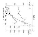
- Figure 1 shows RTP resistivity (µΩ-cm), Si/Mo and deposition rate (angstroms/min) versus deposition temperature. Deposition conditions: 0.25 torr, 4.3 sccm MoF₆, 100 sccm SiH₄. Substrates: thermal oxide - shaded symbols; undoped polysilicon/oxide - open symbols.
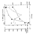
- Figure 2 shows RTP resistivity (µΩ-cm), Si/Mo and deposition rate (anstroms/min) versus deposition temperature. Deposition conditions: 0.28 torr, 3.4 sccm MoF₆, 135 sccm SiH₄. Substrates: thermal oxide - shaded symbols; undoped polysilicon/oxide - open symbols.
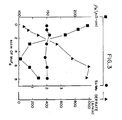
- Figure 3 shows RTP resistivity (µΩ-cm), Si/Mo and deposition rate (angstroms/min) versus MoF₆ flow rate (sccm). Deposition conditions: 0.25 torr, 150°C, 100 sccm SiH₄. Substrates: thermal oxide.
- In a process for the LPCVD of a metal silicide on a substrate ot reduced temperatures, i.e. temperatures at least 100°C below conventional temperatures, it is possible to deposit a metal silicide on a substrate at temperatures ranging from 50°-450°C, depending on the metal and silicon sources, as discussed further below. Reduced temperatures processing is important in that it
- (1) enables the use of lift-off techniques,
- (2) is less likely to redistribute dopants in sub-micron surfaces,
- (3) would enable the application of metal silicides to GaAs technology (in which it is desirable to avoid differential heat stress) as well as to plastics and other temperature-intolerant materials, and
- (4) does not affect aluminium if it is present in the substrate.
- The substrate receiving the metal silicide layer may be any material conventionally used in the electronics industry. A preferred substrate is a single crystal silicon wafer. The substrate may be partially processed, e.g., doped, to provide regions of conductivity. The substrate may have its oxide layer stripped away prior to metal silicide deposition or may still have its oxide layer.
- The substrate is placed in a conventional LPCVD reactor. The reactor contains a pedestal on which the substrate is placed. The pedestal is heated to the desired temperature, depending on the metal compound and silicon compound being used to form the metal silicide layer. The walls of the reactor are cooled either by simply blowing air on the outside walls of the reactor or actively cooling the reactor, such as through the use of a water jacket. The choice between active cooling or simple air cooling is dependent upon the temperature at which the deposition is to occur for the chosen reactants. A lower wall temperature is desired to avoid pre-reaction of the reactants. It has been found that a 50% decrease in deposition rate can occur at processing temperatures if the reactor walls are not cooled. It may also be desirable to cool the gas feed lines and chamber walls below room temperature for a chosen deposition temperature. It is preferred that the reactor be conditioned prior to actual depositions on the substrate. Conditioning can be performed by depositing a metal silicide coating on test substrates. The reactor is periodically cleaned, such as by a NF₃ plasma, to remove buildup of deposited metal silicide.
- Once the substrate has been placed in the reactor the reactor pressure is reduced, typically to the base pressure of the LPCVD system. A pressure of from about 0.05-5 torr may be utilized. It is preferred to use a pressure of 0.2-0.3 torr. If high pressures are used, it may be necessary to utilize a diluent gas to avoid a gas phase reaction which results if higher concentrations of the reactants are present.
- After the desired temperature and pressure conditions have been established, conventional initial CVD purging is preferably used to insure reactor cleanliness. In a preferred embodiment, the reactor is purged with H₂ using a pump and flow purge technique. After the reactor has been purged, it is preferred to bake-out the reactor to remove any water. Although these steps may not be necessary, they are preferred to insure the production of quality products.
- Prior to the introduction of the reactants into the reactor, it is preferred, although not necessary, that the wafer be pretreated by a H₂ plasma treatment. Suitable parameters include a 20-50W, preferably 20W, H₂ plasma treatment at 0.2 torr. The H₂ plasma treatment is desirable to clean the system and to rid the substrate surface of any water. The H₂ plasma treatment may enhance the adhesion of the metal silicide layer to the substrate.
- The reactants are then fed into the reactor through separate feed lines. The reactants are mixed behind a small baffle plate at the entrance. The silicon reactant may be SiH₄ or Si₂H₆, and the metal reactant may be MoF₆, WF₆, TaCl₄ or TiCl₄. MoF₆ may be used with either SiH₄ or Si₂H₆, whereas the other metal reactants may only be used with Si₂H₆. Other combinations do not result in reduced deposition temperatures. The SiH₄ or Si₂H₆ is flowed into the reactor at the rate of 15-145 sccm. The flow rate is considered as the flow rate per wafer. The flow rate for SiH₄ or Si₂H₆ over this range is apparently not critical to the final product. The flow rate of the metal reactant is more critical. If the flow rate is over about 10 sccm, then a pre-reaction will occur. If the flow rate is under about 2 sccm, then the resistivity of the metal silicide coating becomes too high. Thus, the flow rate for the metal reactant should be from about 2 sccm to about 10 sccm. A standard dump is utilized to avoid a burst of the reactants in the reactor.
- The deposition time is generally 2-15 minutes, depending on the desired thickness of the metal silicide layer. A typical deposition time of 4 minutes is used to obtain a 2500 angstrom metal silicide layer at a deposition rate of 700 angstroms/min. The metal silicide layer will preferably have a Si/metal (Si/Me) ratio of from about 1.7-2.3, if a silicon-based substrate is utilized. That is, the metal silicide has the formula MeSix, where 1.7 ≦ x ≦ 2.3. If the substrate is GaAs or a temperature-intolerant material such as plastic, then the ratio can be less than 1.7. In this instance, the maximum ratio is 2.3.
- The temperature to which the substrate is heated is dependent on the reactants which are utilized. If the reactants are MoF₆ and SiH₄, a temperature of about 90°-170°C, preferably 120°-170°C, can be used. In the most preferred embodiment, a temperature of 150°C is utilized. If the reactants are MoF₆ and Si₂H₆, a temperature of about 40°-90°C should be used. When WF₆ and Si₂H₆ are employed as the reactants, a temperature of about 180°-250°C can be used. When TiCl₄ or TaCl₄ and Si₂H₆ are used as the reactants, a suitable temperature would be 350°-500°C, preferably 350°-400°C. The proper temperature is determined for each set of reactants by determining the Si/Me ratio of the film deposited at various temperatures and selecting the temperature range which yields the Si/Me ratio of less than 2.3, as discussed above.
- The invention will be further described by reference to the following non-limiting examples. All temperatures expressed are in degrees Celsius.
- MoSix films were deposited on 4 inch wafers in an air-cooled fused silica bell jar. Wafers were placed on a resistance heated 6 inch fused silica pedestal and heated to 120°-350°C. Wafer temperatures were calibrated with three thermocouple junctions in contact with the top surface of a test wafer; observed temperature variations were ±10°C or less over the wafer.
- SiH₄ and MoF₆ had separate feed lines to the deposition chamber and were mixed behind a small baffle plate at the entrance. The MoF₆ flow was regulated by two needle valves in series and calibrated by filling a known volume. The MoF₆ bottle and valves were housed in a vented 29°C thermostated cabinet. MoF₆ flows in the range from 0.5-10 sccm were reproducible to ±10%. SiH₄ flow was regulated with a 0-300 sccm mass flow controller. Deposition pressures ranged from 0.2-0.3 torr.
- The deposition chamber was pumped with a 27 cfm corrosion-resistant mechanical pump. Oil filters were changed after about 10 µm of deposition. Purging with H₂, pre-deposition bake-out, and minimizing the amount of vacuum system exposed to air during wafer unload/reload kept impurity gas partial pressures, including H₂O, below the 0.1% level. Reactant, product and impurity gases were monitored with a mass spectrometer. The bell jar and heater were periodically cleaned with a NF₃ plasma.
- Rapid thermal processing (RTP) of the MoSix films was performed in a lamp annealer for 30 seconds at 1100°C. Si and Mo content were determined by Rutherford Backscattering (RBS); oxygen impurity was not detected and therefore less than 5%. Thicknesses obtained by black wax masking, 95% HNO₃ + 5% HF etch, and stylus measurement agreed with RBS results and were used to compute deposition rates. Step coverage was determined by SEM of cross sections.
- The deposition temperature dependence of RTP resistivity, Si/Mo ratio and deposition rate is shown for the
range 120°-200°C in Figure 1. All three quantities are approximately constant for temperatures at or below 150°C and then increase in concert as the temperature is raised above 150°C. The reaction between MoF₆ and SiH₄ changes at 150°C when more Si is incorporated into the film as the temperature is increased, resulting in increased deposition rate and resistivity. - With similar MoF₆ and SiH₄ flows, RTP resistivity Si/Mo ratio and deposition rate show consistent increases as the temperature is increased over the
range 150°-350°C (Figure 2). Deposition rate falls off above 250°C, however. This is probably due to reactant loss to gas phase nucleation and/or the observed deposition on the chamber walls. - MoSix film properties as a function of MoF₆ flow at 150°C are illustrated in Figure 3. Deposition rate increases linearly with MoF₆ flow, but the fall-off at higher flows is probably due to gas phase or chamber wall losses. Practically, the same dependence of deposition rate on MoF₆ flow was observed at 250°C. In Figure 3, RTP resistivity shows a minimum at 5 sccm MoF₆, but not because of changes in film composition. The RTP resistivity may be a function of deposition rate-correlated microstructural differences in as-deposited films.
- Si/Mo ratio was determined to be fairly constant for a considerable range of MoF₆ flows (Figure 3) and SiH₄ flows at 150°C. With MoF₆ flow in the range from 3-5 sccm and SiH₄ flow in the range from 15-135 sccm, Si/Mo was 2.0 ± 0.1. Si/Mo ratio by RBS did not change significantly upon RTP (six samples). RTP resistivity at 150°C was also fairly constant at about 120 µΩ-cm for MoF₆ flows above 3 sccm. Data for 250°C samples is less complete, but RTP resistivity shows a minimum as a function of MoF₆ flow similar to that depicted in Figure 3. Furthermore, RTP resistivity is independent of SiH₄ flow at 150°C, but appears to be a moderately increasing function of SiH₄ flow at 250°C.
- Film properties for poly/oxide and oxide coated Si wafers were quite similar. Fifteen samples, deposited under various conditions and temperatures in the range from 120°-300°C, were tape tested before and after RTP annealling. Included were six samples deposited on oxide at 150°C with Si/Mo = 1.9-2.0, and three samples deposited on poly/oxide at 120°C, 130°C and 140°C with respective Si/Mo = 1.7, 1.8 and 1.9. One of the six 150°C samples on oxide was the only tape test failure, but it passed after annealing. Samples were specular and RTP bulk resistivities were typically ten times smaller than as-deposited values.
- This example describes one of the specific trials which followed the procedure of Example 1 and provided the data discussed in Example 1.
- A 4 inch wafer having a poly/oxide coating was stripped for 1 minute in a 10:1 HF dip. The wafer was loaded into the quartz bell jar which was air cooled by blowing air on the exterior of the walls. The bell jar was purged with H₂ for 1 hour by evacuation, flowing in H₂, evacuation, etc. The wafer was then subjected to bake-out for 1 hour with a pedestal temperature of 140°C. The wafer temperature was 150°C. A 20 minute H₂ plasma treatment was then performed at 40W and 0.1 torr. MoF₆ and Si₄ were then flowed into the bell jar with a flow rate of 3.5 sccm and 45 sccm, respectively. Deposition temperatures were 141°C and 150°C, respectively, for the pedestal and wafer. Deposition time was 10 minutes. The Si/Mo ratio of the deposited molybdenum silicide was determined to be 2.0. The deposition rate was 620 angstroms/min. The RTP resistivity of the film was 136 µΩ-cm.
- Two samples were made at 150°C with Si₂H₆ substituted for SiH₄. The molybdenum silicide film which was deposited had Si/Mo ratios of 3 and 4, and RTP resistivities of 430 and 1000 µΩ-cm. These samples correspond to the films produced at 250°-300°C using SiH₄. Since the Si/Mo ratio and RTP resistivity were reduced for MoSix films prepared using MoF₆ and SiH₄ by lowering the temperature, it is anticipated that a lower temperature would produce the desired Si/Mo ratios and RTP resistivity when MoSix films are prepared using MoF₆ and Si₂H₆. A MoSix film having a Si/Mo ratio of 1.7-2.3 is prepared at a deposition temperature from 75°-100°C with active cooling of the chamber walls and gas feed lines.
- The reaction between the refractory metal and silicon in a cold wall system to produce MoSix depends primarily on the metal compound flow and substrate temperature. Using MoF₆ and either SiH₄ or Si₂H₆, deposition temperatures can be utilized which are at least 100°C lower than the WF₆ and SiH₄ cold wall system without loss in purity of the MoSix film and without vacuum system attack. Similar results, i.e., deposition temperatures reduced by about 100°C, can be obtained using WF₆, TaCl₄ or TiCl₄ and Si₂H₆ as the reactant species.
- The principal advantage of the MoF₆ and SiH₄ or Si₂H₆ process over the WF₆ and SiH₄ process is lower temperature. Application to lift-off, a patterning technique which eliminates an etch step, is conceivable. The lower temperature is also less likely to redistribute dopants in sub-micron structures. The latter advantage is also true for use of WF₆, TaCl₄ or TiCl₄ and Si₂H₆.
- MoSix could be deposited on plastics or other temperature-intolerant materials. The LPCVD technique yields better step coverage than physical vapor deposition (PVD) techniques, such as sputtering or evaporation. Therefore, LPCVD MoSix offers an advantage over PVD metallizations on micron-sized (temperature-intolerant) structures. Scintering would likely be impractical for such applications, and some compromise of resistivity would be necessary. The results herein show that 120°C films with x = 1.7 have lower 900 µΩ-cm unscintered resistivity than 1000 µΩ-
cm 150°C films. It is possible that 100°C films would be even more "metal rich" and therefore, more conductive. It is also possible that local laser scintering would lower the resistivity and increase the usefulness of MoSix as a "low temperature" conformal metallization. - A disadvantage of the MoSix films is that they are half as conductive as WSix films after scintering. MoSix films with 1.7≦ x ≦ 2.0 adhere to polysilicon after scintering, while analogous WSix films do not, however. Superior adherence of MoSix with x = 2 on SiO₂ was obtained as well. The superior adherence may be due to less interfilm stress associated with the lower deposition temperature. Lower film stress and metal-rich films (100°C) have potential application to GaAs technology, where rapid scintering may be acceptable.
- The reaction of MoF₆ and SiH₄ to produce MoSix is a viable process for VLSI metallization, yielding a ten-fold increase in conductivity over doped polysilicon after RTP. Si/Me ratios of 2.1-2.2 are desired for refractory metal silicides to avoid abstraction of silicon from surrounding IC structures. A satisfactory Si/Mo ratio in MoSix can be obtained with a substrate temperature of 160°C. At this temperature, one obtains specular films with 70-80% step coverage and 850 angstroms/min. deposition rate. Bulk resistivity of 120 µΩ-cm is twice that of WSix, but adhesion is superior. Furthermore, the process temperature is about 200°C lower than that for WSix. This may enable application to lift-off techniques. Conformal metallization (non-RTP) on plastics or other temperature-intolerant materials could be deposited at temperatures as low as 120°C.
Claims (11)
(a) maintaining the substrate at a temperature of from about 40°C to about 500°C in a reactor whose walls are cooled, and
(b) simultaneously introducing into the reactor a metal compound selected from the group consisting of MoF₆, WF₆, TaCl₄ and TiCl₄ and a silicon compound selected from the group consisting of SiH₄ and Si₂H₆, with the proviso that when the metal compound is WF₆, TaCl₄ or TiCl₄, the silicon compound is Si₂H₆, such that a metal silicide film having a silicon:metal ratio of less than about 2.3 is deposited on said substrate.
Applications Claiming Priority (2)
| Application Number | Priority Date | Filing Date | Title |
|---|---|---|---|
| US06/863,622 US4766006A (en) | 1986-05-15 | 1986-05-15 | Low pressure chemical vapor deposition of metal silicide |
| US863622 | 1986-05-15 |
Publications (2)
| Publication Number | Publication Date |
|---|---|
| EP0245934A2 true EP0245934A2 (en) | 1987-11-19 |
| EP0245934A3 EP0245934A3 (en) | 1988-08-03 |
Family
ID=25341425
Family Applications (1)
| Application Number | Title | Priority Date | Filing Date |
|---|---|---|---|
| EP87302693A Withdrawn EP0245934A3 (en) | 1986-05-15 | 1987-03-27 | Low pressure chemical vapor deposition of metal silicide |
Country Status (3)
| Country | Link |
|---|---|
| US (1) | US4766006A (en) |
| EP (1) | EP0245934A3 (en) |
| JP (1) | JPS62267472A (en) |
Cited By (6)
| Publication number | Priority date | Publication date | Assignee | Title |
|---|---|---|---|---|
| US4871691A (en) * | 1987-11-09 | 1989-10-03 | Etat Francais Centre National de la Recherche Scientifique | Selective deposition process of a refractory metal silicide onto silicon areas |
| EP0363065A3 (en) * | 1988-10-07 | 1990-07-25 | AT&T Corp. | Method for fabricating devices |
| US4957777A (en) * | 1988-07-28 | 1990-09-18 | Massachusetts Institute Of Technology | Very low pressure chemical vapor deposition process for deposition of titanium silicide films |
| EP0443277A1 (en) * | 1990-02-20 | 1991-08-28 | L'air Liquide, Societe Anonyme Pour L'etude Et L'exploitation Des Procedes Georges Claude | Metallized ceramic body and method to make the same |
| US5180432A (en) * | 1990-01-08 | 1993-01-19 | Lsi Logic Corporation | Apparatus for conducting a refractory metal deposition process |
| EP0437110A3 (en) * | 1990-01-08 | 1994-01-05 | Lsi Logic Corp |
Families Citing this family (28)
| Publication number | Priority date | Publication date | Assignee | Title |
|---|---|---|---|---|
| EP0305143B1 (en) * | 1987-08-24 | 1993-12-08 | Fujitsu Limited | Method of selectively forming a conductor layer |
| US5167986A (en) * | 1988-04-15 | 1992-12-01 | Gordon Roy G | Titanium silicide-coated glass windows |
| US4853347A (en) * | 1988-10-03 | 1989-08-01 | Motorola, Inc. | Selective metal deposition process |
| KR930002673B1 (en) * | 1990-07-05 | 1993-04-07 | 삼성전자 주식회사 | Growing method of metal having high melting point |
| US5240739A (en) * | 1992-08-07 | 1993-08-31 | Micron Technology | Chemical vapor deposition technique for depositing titanium silicide on semiconductor wafers |
| KR950009934B1 (en) * | 1992-09-07 | 1995-09-01 | 삼성전자주식회사 | Metalizing method of semiconductor device |
| US5380566A (en) * | 1993-06-21 | 1995-01-10 | Applied Materials, Inc. | Method of limiting sticking of body to susceptor in a deposition treatment |
| US5378654A (en) * | 1994-05-24 | 1995-01-03 | United Microelectronics Corporation | Self-aligned contact process |
| US5554566A (en) * | 1994-09-06 | 1996-09-10 | United Microelectronics Corporation | Method to eliminate polycide peeling |
| US5633036A (en) * | 1995-04-21 | 1997-05-27 | The Board Of Trustees Of The University Of Illinois | Selective low temperature chemical vapor deposition of titanium disilicide onto silicon regions |
| US5908659A (en) * | 1997-01-03 | 1999-06-01 | Mosel Vitelic Inc. | Method for reducing the reflectivity of a silicide layer |
| US6162715A (en) * | 1997-06-30 | 2000-12-19 | Applied Materials, Inc. | Method of forming gate electrode connection structure by in situ chemical vapor deposition of tungsten and tungsten nitride |
| TW396646B (en) | 1997-09-11 | 2000-07-01 | Lg Semicon Co Ltd | Manufacturing method of semiconductor devices |
| KR100425147B1 (en) * | 1997-09-29 | 2004-05-17 | 주식회사 하이닉스반도체 | Method for manufacturing semiconductor device |
| JP3191290B2 (en) * | 1999-01-07 | 2001-07-23 | 日本電気株式会社 | Semiconductor device manufacturing method and plasma CVD apparatus used in semiconductor device manufacturing method |
| US6613695B2 (en) * | 2000-11-24 | 2003-09-02 | Asm America, Inc. | Surface preparation prior to deposition |
| US6960537B2 (en) | 2001-10-02 | 2005-11-01 | Asm America, Inc. | Incorporation of nitrogen into high k dielectric film |
| US6586330B1 (en) * | 2002-05-07 | 2003-07-01 | Tokyo Electron Limited | Method for depositing conformal nitrified tantalum silicide films by thermal CVD |
| US6995081B2 (en) * | 2002-08-28 | 2006-02-07 | Micron Technology, Inc. | Systems and methods for forming tantalum silicide layers |
| US6967159B2 (en) * | 2002-08-28 | 2005-11-22 | Micron Technology, Inc. | Systems and methods for forming refractory metal nitride layers using organic amines |
| US6794284B2 (en) * | 2002-08-28 | 2004-09-21 | Micron Technology, Inc. | Systems and methods for forming refractory metal nitride layers using disilazanes |
| US7727588B2 (en) * | 2003-09-05 | 2010-06-01 | Yield Engineering Systems, Inc. | Apparatus for the efficient coating of substrates |
| US7521356B2 (en) * | 2005-09-01 | 2009-04-21 | Micron Technology, Inc. | Atomic layer deposition systems and methods including silicon-containing tantalum precursor compounds |
| US8557702B2 (en) | 2009-02-02 | 2013-10-15 | Asm America, Inc. | Plasma-enhanced atomic layers deposition of conductive material over dielectric layers |
| US20180312966A1 (en) * | 2015-10-23 | 2018-11-01 | Applied Materials, Inc. | Methods For Spatial Metal Atomic Layer Deposition |
| US10312096B2 (en) | 2016-12-12 | 2019-06-04 | Applied Materials, Inc. | Methods for titanium silicide formation using TiCl4 precursor and silicon-containing precursor |
| CN111194361B (en) * | 2017-10-09 | 2022-12-13 | 应用材料公司 | Conformal doped amorphous silicon as nucleation layer for metal deposition |
| US20240387190A1 (en) * | 2023-05-15 | 2024-11-21 | Applied Materials, Inc. | Formation of silicon-and-metal-containing materials for hardmask applications |
Family Cites Families (8)
| Publication number | Priority date | Publication date | Assignee | Title |
|---|---|---|---|---|
| US4359490A (en) * | 1981-07-13 | 1982-11-16 | Fairchild Camera & Instrument Corp. | Method for LPCVD co-deposition of metal and silicon to form metal silicide |
| US4565157A (en) * | 1983-03-29 | 1986-01-21 | Genus, Inc. | Method and apparatus for deposition of tungsten silicides |
| US4557943A (en) * | 1983-10-31 | 1985-12-10 | Advanced Semiconductor Materials America, Inc. | Metal-silicide deposition using plasma-enhanced chemical vapor deposition |
| US4629635A (en) * | 1984-03-16 | 1986-12-16 | Genus, Inc. | Process for depositing a low resistivity tungsten silicon composite film on a substrate |
| US4504521A (en) * | 1984-03-22 | 1985-03-12 | Rca Corporation | LPCVD Deposition of tantalum silicide |
| DE3413064A1 (en) * | 1984-04-06 | 1985-10-31 | Siemens AG, 1000 Berlin und 8000 München | METHOD FOR PRODUCING METAL SILICIDE LAYERS BY DEPOSITION FROM THE GAS PHASE WITH REDUCED PRESSURE AND THE USE THEREOF |
| US4568565A (en) * | 1984-05-14 | 1986-02-04 | Allied Corporation | Light induced chemical vapor deposition of conductive titanium silicide films |
| JPS61221376A (en) * | 1985-03-27 | 1986-10-01 | Hitachi Ltd | Formation of thin metallic film |
-
1986
- 1986-05-15 US US06/863,622 patent/US4766006A/en not_active Expired - Fee Related
-
1987
- 1987-03-27 EP EP87302693A patent/EP0245934A3/en not_active Withdrawn
- 1987-05-11 JP JP62112647A patent/JPS62267472A/en active Pending
Cited By (8)
| Publication number | Priority date | Publication date | Assignee | Title |
|---|---|---|---|---|
| US4871691A (en) * | 1987-11-09 | 1989-10-03 | Etat Francais Centre National de la Recherche Scientifique | Selective deposition process of a refractory metal silicide onto silicon areas |
| US4957777A (en) * | 1988-07-28 | 1990-09-18 | Massachusetts Institute Of Technology | Very low pressure chemical vapor deposition process for deposition of titanium silicide films |
| EP0363065A3 (en) * | 1988-10-07 | 1990-07-25 | AT&T Corp. | Method for fabricating devices |
| US5180432A (en) * | 1990-01-08 | 1993-01-19 | Lsi Logic Corporation | Apparatus for conducting a refractory metal deposition process |
| EP0437110A3 (en) * | 1990-01-08 | 1994-01-05 | Lsi Logic Corp | |
| US5391394A (en) * | 1990-01-08 | 1995-02-21 | Lsi Logic Corporation | Tungsten deposition process for low contact resistivity to silicon |
| EP1069207A3 (en) * | 1990-01-08 | 2003-05-14 | Lsi Logic Corporation | In-situ etch method for for cleaning a CVD chamber |
| EP0443277A1 (en) * | 1990-02-20 | 1991-08-28 | L'air Liquide, Societe Anonyme Pour L'etude Et L'exploitation Des Procedes Georges Claude | Metallized ceramic body and method to make the same |
Also Published As
| Publication number | Publication date |
|---|---|
| EP0245934A3 (en) | 1988-08-03 |
| US4766006A (en) | 1988-08-23 |
| JPS62267472A (en) | 1987-11-20 |
Similar Documents
| Publication | Publication Date | Title |
|---|---|---|
| US4766006A (en) | Low pressure chemical vapor deposition of metal silicide | |
| US4557943A (en) | Metal-silicide deposition using plasma-enhanced chemical vapor deposition | |
| EP0599991B1 (en) | Process for forming low resistivity titanium nitride films | |
| US10854461B2 (en) | Tungsten deposition without barrier layer | |
| US5252518A (en) | Method for forming a mixed phase TiN/TiSi film for semiconductor manufacture using metal organometallic precursors and organic silane | |
| US6313035B1 (en) | Chemical vapor deposition using organometallic precursors | |
| EP0414267B1 (en) | Process for deposition of a tungsten layer on a semiconductor wafer | |
| US6210813B1 (en) | Forming metal silicide resistant to subsequent thermal processing | |
| US6903010B2 (en) | Low-resistance contact to silicon having a titanium silicide interface and an amorphous titanium carbonitride barrier layer | |
| US5733816A (en) | Method for depositing a tungsten layer on silicon | |
| US5723382A (en) | Method of making a low-resistance contact to silicon having a titanium silicide interface, an amorphous titanium nitride barrier layer and a conductive plug | |
| JPH0773102B2 (en) | Chemical vapor deposition technique for depositing titanium silicide on semiconductor wafers. | |
| KR100187451B1 (en) | Manufacturing method of titanium nitride thin film | |
| Chiou et al. | The processing windows for selective copper chemical vapor deposition from Cu (hexafluoroacetylacetonate) trimethylvinylsilane | |
| WO1998028783A1 (en) | Method of nucleation used in semiconductor devices | |
| EP0591086A2 (en) | Low temperature chemical vapor deposition and method for depositing a tungsten silicide film with improved uniformity and reduced fluorine concentration | |
| JP7542046B2 (en) | Tungsten Deposits Without Barrier Layers | |
| US4794019A (en) | Refractory metal deposition process | |
| US6168837B1 (en) | Chemical vapor depositions process for depositing titanium silicide films from an organometallic compound | |
| Hara et al. | Tungsten Silicide Films Deposited by SiH2Cl2‐WF 6 Chemical Reaction | |
| JPS63109172A (en) | Low pressure chemical vapor deposition of metal silicide | |
| JPH10209073A (en) | Method of forming barrier film | |
| WO2019213339A1 (en) | Methods and apparatus for high reflectivity aluminum layers | |
| JP3953244B2 (en) | Thin film formation method | |
| KR940010158B1 (en) | Tungsten Thin Film Deposition Method by Plasma Chemical Vapor Deposition |
Legal Events
| Date | Code | Title | Description |
|---|---|---|---|
| PUAI | Public reference made under article 153(3) epc to a published international application that has entered the european phase |
Free format text: ORIGINAL CODE: 0009012 |
|
| AK | Designated contracting states |
Kind code of ref document: A2 Designated state(s): DE FR GB |
|
| PUAL | Search report despatched |
Free format text: ORIGINAL CODE: 0009013 |
|
| RHK1 | Main classification (correction) |
Ipc: H01L 21/285 |
|
| AK | Designated contracting states |
Kind code of ref document: A3 Designated state(s): DE FR GB |
|
| 17P | Request for examination filed |
Effective date: 19881221 |
|
| 17Q | First examination report despatched |
Effective date: 19900607 |
|
| STAA | Information on the status of an ep patent application or granted ep patent |
Free format text: STATUS: THE APPLICATION IS DEEMED TO BE WITHDRAWN |
|
| 18D | Application deemed to be withdrawn |
Effective date: 19901218 |
|
| RIN1 | Information on inventor provided before grant (corrected) |
Inventor name: GACZI, PETER J. |