EP0245564B1 - Multi-Port-Speicher und Quelleneinrichtung für Bildpunktinformation - Google Patents
Multi-Port-Speicher und Quelleneinrichtung für Bildpunktinformation Download PDFInfo
- Publication number
- EP0245564B1 EP0245564B1 EP86400976A EP86400976A EP0245564B1 EP 0245564 B1 EP0245564 B1 EP 0245564B1 EP 86400976 A EP86400976 A EP 86400976A EP 86400976 A EP86400976 A EP 86400976A EP 0245564 B1 EP0245564 B1 EP 0245564B1
- Authority
- EP
- European Patent Office
- Prior art keywords
- shift register
- bit map
- map memory
- information
- pixel information
- Prior art date
- Legal status (The legal status is an assumption and is not a legal conclusion. Google has not performed a legal analysis and makes no representation as to the accuracy of the status listed.)
- Expired
Links
- 230000015654 memory Effects 0.000 title claims abstract description 129
- 230000002093 peripheral effect Effects 0.000 claims abstract description 6
- 230000000873 masking effect Effects 0.000 claims description 18
- 230000001419 dependent effect Effects 0.000 claims 2
- 230000002457 bidirectional effect Effects 0.000 abstract description 11
- 230000005540 biological transmission Effects 0.000 abstract description 4
- 230000000694 effects Effects 0.000 description 14
- 230000004044 response Effects 0.000 description 13
- 238000000034 method Methods 0.000 description 5
- 230000001143 conditioned effect Effects 0.000 description 4
- 230000003111 delayed effect Effects 0.000 description 3
- 238000010586 diagram Methods 0.000 description 3
- 239000003973 paint Substances 0.000 description 3
- 239000004065 semiconductor Substances 0.000 description 3
- 238000004519 manufacturing process Methods 0.000 description 2
- 239000013078 crystal Substances 0.000 description 1
- 238000010894 electron beam technology Methods 0.000 description 1
- 238000005530 etching Methods 0.000 description 1
- 230000005764 inhibitory process Effects 0.000 description 1
- 238000003860 storage Methods 0.000 description 1
Images


Classifications
-
- G—PHYSICS
- G09—EDUCATION; CRYPTOGRAPHY; DISPLAY; ADVERTISING; SEALS
- G09G—ARRANGEMENTS OR CIRCUITS FOR CONTROL OF INDICATING DEVICES USING STATIC MEANS TO PRESENT VARIABLE INFORMATION
- G09G5/00—Control arrangements or circuits for visual indicators common to cathode-ray tube indicators and other visual indicators
- G09G5/34—Control arrangements or circuits for visual indicators common to cathode-ray tube indicators and other visual indicators for rolling or scrolling
- G09G5/346—Control arrangements or circuits for visual indicators common to cathode-ray tube indicators and other visual indicators for rolling or scrolling for systems having a bit-mapped display memory
-
- G—PHYSICS
- G09—EDUCATION; CRYPTOGRAPHY; DISPLAY; ADVERTISING; SEALS
- G09G—ARRANGEMENTS OR CIRCUITS FOR CONTROL OF INDICATING DEVICES USING STATIC MEANS TO PRESENT VARIABLE INFORMATION
- G09G5/00—Control arrangements or circuits for visual indicators common to cathode-ray tube indicators and other visual indicators
- G09G5/36—Control arrangements or circuits for visual indicators common to cathode-ray tube indicators and other visual indicators characterised by the display of a graphic pattern, e.g. using an all-points-addressable [APA] memory
- G09G5/39—Control of the bit-mapped memory
-
- G—PHYSICS
- G09—EDUCATION; CRYPTOGRAPHY; DISPLAY; ADVERTISING; SEALS
- G09G—ARRANGEMENTS OR CIRCUITS FOR CONTROL OF INDICATING DEVICES USING STATIC MEANS TO PRESENT VARIABLE INFORMATION
- G09G5/00—Control arrangements or circuits for visual indicators common to cathode-ray tube indicators and other visual indicators
- G09G5/36—Control arrangements or circuits for visual indicators common to cathode-ray tube indicators and other visual indicators characterised by the display of a graphic pattern, e.g. using an all-points-addressable [APA] memory
Definitions
- the invention is described with reference to its use in a video display device but other output devices, such as printers which handle serial information, can employ the present invention.
- the pixel information in the bit map memory can be read out to paint the picture, or to paint an alpha-numeric display, on the screen, without necessitating a great number of manipulations of information, and accordingly very rapidly.
- the state of the art has advanced such that pixel information is available (and desirable) from a number of pixel information input means.
- a major problem is that the pixel information sources operate at different speeds and very often the information signals are burdened with phase distortion, jitter, timing irregularities and the like. If such information is transmitted directly from the source to the video display, the picture provided to the viewer is often unsatisfactory.
- a raster graphics display refresh memory architecture incorporating two shift registers connected to receive pixel information from a memory is disclosed in the American patent 4,546,451 to Bruce.
- the display refresh shift register shifts out pixel information in response to a VIDEO CLOCK signal to produce the video output for refreshing the CRT display.
- the screen readback shift register shifts out pixel information in response to a GCD CLOCK signal to produce the data for manipulation by the graphics computation device.
- No masking means is disclosed in that prior patent, which in an important difference from the invention as defined in claim 1.
- the bit map memory of Bruce comprises a plurality of separate chips and the shift register means of Bruce likewise comprises a plurality of chips. Bruce does not disclose the provision of circuit arrangement on an integrated chip, as recited in claim 2.
- Mask means are included in bidirectional data transmission channels connecting the shift register means to the bit map memory means. Accordingly pixel information can be masked en route and thus only certain pixel bits are loaded into bit map memory. Alternatively, only certain pixel bits are read from the bit map memory to effect such operation as window scrolling or a split-screen presentation.
- the invention generally concerns a circuit arrangement for storing pixel information and outputting signals representing said stored pixel information for display, comprising bit map memory means having an array of row and column positions for storing said pixel information thereat, said bit map memory means having a plurality of data ports, first control means connected to said bit map memory means for enabling the input and output of pixel and masking information to and from predetermined addresses in said bit map memory means, first shift register means for shifting pixel information stored therein, said first shift register means having a plurality of data ports connected to said plurality of data ports of said bit map memory means by way of first gating means, a mask register means for storing masking information, said mask register means being connected to said plurality of data ports of said bit map memory means by way of a second gating means, said first and second gating means being connected to a second control means for controlling the gating of said first and second gating means, and said mask register means being connected to said first gating means, wherein said second control means is capable of outputting a first
- the preferred embodiment of the present invention is formed on an integrated circuit chip.
- the technique for producing integrated circuit memory devices, logic devices, active and passive elements and shift registers is well understood in the art of fabricating integrated circuits. Instruction information for fabricating such circuits can be found, for instance, in the text "Physics and Technology of Semiconductor Devices” by Andrew Grove, as well as in the text "Introduction to VLSI Systems” by Carver Mead and Lynn Conway.
- the present invention resides in the architecture of the circuitry and not in the fabrication of the integrated circuit chip per se. However, since the architecture enables the circuitry to be readily made part of an integrated circuit and enhances the data handling of pixel signals, the use of the present invention as provided in integrated circuit form is a substantial advance in the art.
- circuitry and its operation will be described as if the components were hard-wired on a circuit board.
- the present system could be a hard-wired set of components, or one or more hybrid circuit boards, and could employ core memories, transistor logic memories, etc.
- Figure 2 the elements of the present system which are mounted on an integrated circuit chip are shown.
- the fabrication of the integrated circuits employed in the present system it should be pointed out that in order for 256 lines to be arranged as input/output channels, to and from a bit map memory unit, it was necessary to extend the digit lines beyond the physical positions of the decoder circuits found on a commercially available chip. The foregoing is accomplished by employing a technique of etching a polysilicone layer whereby the digit lines are extended.
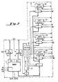
- Figure 1 shows a large bit map memory 11, a data processor 13 and a block of logic and control circuitry 15.
- four extended shift registers 17, 19, 21 and 23 are provided, each of which has an input means and an output means as depicted by the double-arrowed channels 25, 27, 29 and 31.
- Channels 25, 27, 29 and 31 are respectively connected to peripherals 33, 35, 37, and 39 (denoted by dashed lines to indicate that they are not part of the invention).
- the overall system of Figure 1 operates as follows.
- Information to be shown on a high-resolution video display 33 can be transmitted from the data processor 13 by way of the logic circuitry 15 to the large bit map memory 11. Said information thereafter can be addressed by the data processor 13 and transferred along channels 41 and 43, through logic circuitry 45, along channel 47, to the shift register 17.
- Shift register 17 is conditioned to accept said information by control signals on channel 49. Thereafter the shift register 17 serially transfers said information along channel 25 to the high-resolution video display 33.
- the information just described represents window information, i.e. less than a whole screen display
- some of the information bit signals are inhibited by logic circuitry 45 and other bit signals are passed.
- This partial inhibition is effected by masking information in the mask register 51.
- the system Prior to passing the information from the large bit map memory 11 to the shift register 17, the system, under the direction of the data processor 13, transfers masking data from the bit map memory 11 to the masking register 51 along channels 41 and 53. Thereafter, and in response to control signals from the logic circuitry 15, the masking information is transferred to logic circuitry 45 and controls certain gates therein to inhibit the flow of certain bit signals therethrough, to effect the window display.
- the shift register 19 is arbitrarily assigned to handle pixel information for a slow-speed video display 35.
- Information to be shown on the slow-speed video display can be loaded into the shift register 19 from the data processor 13 by way of the bit map memory 11 from any of the shift registers 17, 21 and 23, a transfer of said information into and out of the large bit map memory; or from an outside peripheral connected to its serial input means.
- the shift register 21 has been arbitrarily assigned the role of accepting information signals from a slow-speed source, such as a disk, camera, tape or the like. If the information received by the shift register 21 were to be displayed on the low-speed video, it would be transferred to the shift register 19 along a route (composed of channels 55, 47, 43 and 41) into and out of the bit map memory 11, in a fashion similar to that just described. If that information were burdened, as often is the case, with phase distortion, jitter or timing irregularities, such information would be loaded into the shift register 21 and held there momentarily while the irregularities settled down. Thereafter that same information would be transferred in good form as just described, to be seen on the low-speed video display 35. If such information were intended to be seen on the high-resolution video display, the information would be transferred to the shift register 17.
- a slow-speed source such as a disk, camera, tape or the like.
- the shift register 23 has been arbitrarily assigned to handle information which is going to be used in scrolling presentations or window presentations.
- the shift register 23 can be activated to shift right or left, and hence information bits which need to be located in new positions in the right or left sense are manipulated in this shift register.
- information is loaded into the shift register 23 from a certain address in the bit map memory 11 and is returned to the bit map memory at a new address so that the viewer sees the text, or picture, gently moving up (and possibly off) the screen.
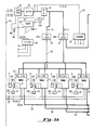
- Figure 2 shows the system elements coupled together on an integrated circuit chip.
- the elements shown in Figure 2 are the same as those shown in Figures 3A and 4A to be discussed below. However, some differences should be noted.
- Figure 2 shows a mask register 57 associated with the shift register units 64, 65, 67 and 69. In the system there is one mask register for each chip and hence for each vertically (in the drawings) associated set of four shift register units. However, in the description of figures 3A and 4A only one mask register is discussed. Only one mask register is shown to simplify the drawing but theoretically the system operates in the same manner with the one mask register as it would with four mask registers.
- Each chip also has an RA latch, a CA latch and a decoder. The description of Figures 3A and 4A discusses only one such RA latch 59, CA latch 61 and decoder 63, however the arrangement would be the same if four of each were used.
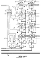
- Figure 3A shows a preferred embodiment with four bit map memory units 71, 73, 75 and 77, which are similar to the integrated circuit chips manufactured by Micron Technology Corporation and designated as MT4264 but are altered as described above and as shown in Figure 2.
- Each bit map memory unit has 256 columns and 256 rows.
- Figure 4A shows bit map memory units 78 through 89.
- the bit map memory units 71, 73, 75, 77 and 78-89 together represent a large bit map memory having 1024 rows and 1024 columns.
- the preferred embodiment accommodates a high-resolution display device 91, shown in Figure 3B, which has 1024 column positions and 660 row positions.
- rows 661 through 1024 contain information which does not appear on the screen during a display. That information is used to effect operations such as masking and font character storage.
- bit map memory units each contain two logic means for decoding as well as a logic means to effect read/write (write enable) operations.
- the logic circuitry to the right decodes the column addresses, while the logic circuitry to the left decodes the row address information.
- the decoding logic circuitry, as well as the write enable logic circuitry is part of the commercially available bit map memory (mentioned above) and no further description of such an operation is deemed necessary.
- the embodiment presented herein is related to a high-resolution display having 1024 columns and 660 row positions, in accordance with the invention other configurations could be used. Also other bit map memory unit sizes could be employed.
- the data processor 93 may be any well-known data processor having the capability of being programmable, handling such programs, and providing data information, instruction information, and address information. If we assume that the data processor has been programmed to transfer information into the large bit map memory, then the information will be loaded into the bit map memory at some column address and some row address and accordingly the data processor 93 will transmit both column address signals and row address signals to the buffer 95. Part of the address signals will be transmitted from the buffer 95 to the row address (RA) latch 59 and to the column address (CA) latch 61 through the multiplexer (MUX) 97. Two bits of the row address are sent directly to the decoder 99 while three bits of the column address are sent to decoder 101. MUX 97 can be any well-known multiplexer such as a 74F157 manufactured by Fairchild Semiconductor Corporation.
- the multiplexer 97 separates the column address signals and the row address signals.
- the column address signals are transmitted to the CA latch 61, while the row address signals are transmitted to the RA latch 59.
- the latches 59 and 61 can each be a 74F374 manufactured by Fairchild Semiconductor Co. or a similar device.
- a row address strobe (RAS) signal is transmitted from the timing generator to the RA latch 59 and a column address strobe (CAS) signal is transmitted to the CA latch 61.
- the address information comprises a 20-bit address on line 107. Bits 0 through 6 of the address are decodable to provide the column address. Bit 7 indicates whether the system is in a random access mode or a register mode of operation.
- Bits 8 and 9 used to determine which of the bit map memory units is to receive the column address information.
- the second ten bits of the address information include bits 10 through 17 to determine the row address within the bit map memory, and bits 18 and 19 to determine which one of the rows of bit map memory units, such as the rows starting respectively with bit map memory units 71, 78, 82 and 86, is to receive the row address information.
- the system needs only 7 bits to determine the column address but needs 8 bits to determine the row address because the data processor 93 transmits (or reads) two bits for two column positions, at one time, in response to a single column address. In other words, if the column address is "zero", one bit in column 1 and one bit in column 2 will be transmitted to or selected from the bit map memory.
- the 20-bit address signals are transmitted on line 107 to the MUX 97.
- the MUX 97 is controlled by a delayed RAS signal.
- bits 10 through 17 are transmitted to both latches 59 and 61.
- only latch 59 will be enabled to store the bits 10 through 17.
- Latches 59 and 61 only respond to leading edge changes in control signals.
- bits 0-7 are transmitted to both latches 59 and 61.
- only latch 61 will be enabled (by the leading edge of the CAS signal) to store bits 0 through 7.
- Bits 7, 8 and 9 are transmitted on line 109 to the decoder 101.
- bit 7 If the bit 7 is high, then all of the column lines are activated because bit 7 in its high form indicates a register mode and hence every bit in the row selected by the row address should be transferred from the bit map memory unit. If the bit 7 is low, the system is in a random access mode and the column of bit map memory units selected by decoding bits 8 and 9 receives the column address signals from latch 61. Accordingly the decoder 101 transmits one of four signals on the lines H, J, K and L, which lines respectively go to logic gates 111, 113, 115 and 117. Hence one of those gates is fully enabled and passes the CAS signal, which in turn causes the logic within the bit map memory unit to permit bits 0-6 to select a column address in the correct bit map memory unit.
- the eight bits 10 through 17 which make up the row address are transmitted to the latch 59 as described above.
- the bits 18 and 19 are separately transmitted on line 119 to the decoder 99.
- the row address signals are transmitted from RA latch 59 to the decoders of the respective bit map memories 71, 73, 75 and 77.
- row address information is transmitted to similar logic gates associated with the bit map memory units 78 through 89.
- the same row address information will be sent to each of the bit map memory units in a row.
- the large bit map memory includes (collectively) the 256 bits of each of the bit map memory units 71, 73, 75 and 77 to provide 1024 column positions.
- the decoder 99 provides enabling signals A, B, C and D to the bit map memories, which signals determine which one of the rows of bit map memory units will respond to the row address information. For instance, the A signal to logic circuit 121 permits the RAS signal to pass to the internal logic, which causes the bit map memory unit 71 to respond to the row address signals at decoder 123.
- Two lines 125 are connected to the data processor 93.
- the designations DI/01 and DI/02 stand for data input/output one and data input/output two.
- the present system uses a two-bit simultaneous input from the data processor for two reasons.
- the data processor is a 16-bit word data processor.
- the DI/01 and DI/02 signals are transmitted over the lines 125 to the lines 127, 129 and 131, and then to each bit map memory unit.
- the information from lines 125, going to the bit map memory units, is available to each pair of column lines in each bit map memory.
- only the column lines selected by the column address actually participate in the read or write operation. This procedure is well understood in the data processing art and no further description of that operation is necessary.
- In the large bit map memory there is a position for every pixel position on the high-resolution screen of device 91.
- the information to paint that display can be read into the bit map memory from the data processor through the DI/01 and DI/02 lines.
- Channels 133, 135, 137 and 139 are respectively connected to bit map memories 71, 73, 75 and 77.
- Each of these channels is made up of 256 lines so that during readout from a bit map memory unit, 256 bits can be read onto the channel and transmitted therefrom to the shift register structure as shown in Figure 3B. If readout of the row of bit map memory units in Figure 3A is to be effected, then the row address signals will be transmitted to the bit map memory, in particular to decoder 123 as well as the column address bit 7, equal to a logic ONE.
- the write enable signal transmitted to the logic circuitry 141 will be high to effect the readout. In addition, the logic circuitry 121 will be fully enabled.
- the 256 bits will be transmitted over channel 133 to the two logic circuit blocks 143 and 145. If the information read from the bit map memory unit 71 is "mask information", then logic circuitry 143 will be enabled by a signal on line 147, and the 256 bits will be transmitted into the mask register 57. Such mask information will be used to condition a plurality of gates (during the presence of a control signal on line 149) in the logic circuit 145 to enable certain of the signals on channel 133 to be transmitted therethrough and to inhibit the remaining signals. While the same information is transmitted through the gates 145 and along the channel 151, none of the logic circuits 153, 155, 157 and 159 will be enabled to transmit that information therethrough to the associated shift register units.
- logic circuit 153 would be conditioned by a signal on line 161 to transmit that information therethrough and the 256 bits would be loaded, in parallel, into shift register unit 64.
- the 8-bit address signals (bits 0-7) transmitted to the column address latch 61 serve a multiple purpose. In one mode these signals are column address signals, while in another mode these signals are decoded to determine which shift register will receive information; whether the mask register 57 will receive mask information; whether the mask information is to be used at logic circuit 145; and which direction, right or left, shift register 163 is to be shifted. Seven lines 165 leave decoder 63. The signals on those lines are generated in response to the decoding of bits 0-7 of the column address information which are transmitted to the column address latch 61. If bit 7 is a ONE, decoder 63 will provide signals on lines 165. The bit 7 signal also renders all of the column lines active.
- the data processor When the data processor is effecting a readout from the bit map memory to the shift register, it also takes into consideration which shift registers that information is to be transmitted to. For instance, if such information is to be transmitted to shift register unit 64, then the bits transmitted to decoder 63 will be decoded to provide a signal on the enable line 161 which will enable logic circuitry 153 to transmit the 256 bits to shift register 64.
- the enabling or control signals on lines 147, 149, 167, 169, 171, and 173 are generated in a similar manner to that described for the enabling signal on line 161.
- the decoder 63 is shown as having output lines to each of the logic gates connected to the shift register units. There is a decoder 63 on each integrated circuit chip, as shown in Figure 2. Each integrated circuit chip also has its own RA latch 59 and CA latch 61.
- the shift register units are arranged to form extended shift registers.
- the extended shift register made up of shift register units 64, 175, 177 and 179 is the high-speed extended shift register 181. Adjacent shift register units are coupled by two lines.
- the structure of one of the shift register units is shown in Fig. 6.
- a 20-MHz clock signal is transmitted on line 183.
- Figure 7 shows the relationship between the 20, 40 and 80 MHz clock signals.
- Figure 6 shows four shift register subunits, each of which has 64 bits of information therein. Together the four shift register subunits act as one shift register unit which is capable of handling 256 bits.
- shift register subunits 185, 187, 189 and 191 can be read out in response to a 20-MHz clock signal on line 183.
- the shift register subunits 185 and 191 respond to the leading edges 197 of the 20-MHz clock signal (see Figure 7) by shifting one bit position at a time, respectively, onto lines 193 and 195.
- the trailing edge 198 of the 20-MHz clock signal ( Figure 7) is inverted at the inverter 199 ( Figure 6) to provide a leading edge signal to the shift register subunits 187 and 189, in response to which one bit position is shifted at a time, respectively, onto lines 201 and 203.
- a bit signal on line 201 is immediately transmitted through the MUX 205 to output line 207 at the time when the leading edge 197 arrives.
- the MUX 205 receives the bit signals present on line 193 at the time when the trailing edge 198 arrives so that the signals output on line 207 appear at a rate of 40 MHz, as indicated by the trailing edges 209 and 211 in Figure 7.
- the times of the trailing edges 209 and 211 are the times that respective signals from shift register subunits 185 and 187 appear on line 207. Accordingly shift register subunits 185 and 187, although they are clocked out at a 20-MHz rate (in the arrangement shown in Figure 6), provide a 40-MHz output train of signals on line 207.
- the shift register subunits 189 and 191 are clocked to provide a train of bits on line 213 which are transmitted at a 40-MHz rate.
- Figure 6 also shows terminals 215 and 217.
- Terminal 215 is connected to transmit information to shift register subunits 185 and 187. The information is clocked into those subunits by the 20-MHz clock signal as just described.
- terminal 217 is connected to transmit information to subunits 189 and 191, which information is clocked into those shift register subunits as described above.
- the output signals on lines 207 and 213 are connected to terminals in the next shift register unit similar to terminals 215 and 217.
- Figure 3B1 in which shift register unit 64 is shown connected through two lines to shift register 175, which is in turn connected through two lines to shift register unit 177, and so forth.
- the two lines in Figure 3B1 are similar to lines 207 and 213.
- each shift register unit includes the MUX device as well as the inverter of Figure 6.
- the final output signals on lines 219 and 221 are transmitted to an ECL shift register 223 (for example 10141 manufactured by Fairchild Semiconductor Company).
- the ECL shift register 223 operates such that in response to the leading edge of a signal on the F terminal, with the E terminal low, the ECL logic will load a bit signal from line 219 onto the output line 225. On the other hand, in response to the leading edge of a signal on the F terminal, with the E terminal high, a bit signal from line 221 will be shifted onto line 225.
- the signal connected to the F terminal is at 80 MHz and that connected to the E terminal is at 40 MHz.
- the ECL shift register will load bit signals from line 219 as well as from line 221, via the logic within the block, onto the output line 225.
- the bit signals from line 219 are transferred to line 225, whereas at the leading edges 229 and 233 the bit signals from line 221 are transferred to line 225.
- the output on line 225 is an 80-MHz train of bit signals, which is a rate sufficient to accommodate the high-resolution display device 91.
- Figure 4B shows the other three high-speed extended shift registers, which provide the same kind of outputs as are available on line 225 ( Figure 3B2) on lines S, U, and W.
- the 80-MHz output signals on line S, U, and W are transmitted to the MUX 235 and therefrom to the high-resolution display device 91.
- the MUX 235 is controlled by the output of decoder 237 by way of latch 238, which passes the control signals in response to the enable signal on line 161.
- the output from decoder 99 selects which of the rows of bit map memory units is to be operative. Hence, the output from decoder 99 selects which of the lines S, U or V is to be selected by MUX 235.
- the enable signal on line 161 indicates that the high-speed shift register is addressed. Accordingly, although the extended shift register is clocked at a 20-MHz rate, it has an output at 80-MHz which provides bit signals having the density necessary to accommodate the high-resolution display device 91.
- bit map memory unit 71 The output signals on channel 133 from bit map memory unit 71 will be discussed by way of example, although the other bit map memories operate in a similar manner. If the user of the system decides, through the data processor, that the information should be transmitted into shift register unit 65 ( Figure 3B1), then the 256 bits transmitted along channel 151 are routed to the logic circuit 155. Logic circuit 155 is enabled by enabling signal 167 and hence the 256 bits are parallel loaded into shift register unit 65.
- Each of the extended shift registers has a different clock input labelled G, P, N or M, these clock signals being at different clock rates depending upon the use of the extended shift register. In a preferred embodiment the clock signal P, N, and M have respective rates of 22, 14 and 25 MHz.
- Timing circuits 239, 241, and 243 ( Figure 4B), which can be similar to the circuit shown in Figure 10.
- Timing circuit 241 generates a sync 1 signal which can be used with an input device connected to terminal 245 ( Figure 3B1).
- Timing circuit 239 generates a sync 2 signal which is used with display device 247.
- the shift registers 249, 251, 253 and 255 are series-connected to form extended shift register 257, which is in general assigned the job of providing relatively low-speed output information to a low-resolution data display device 247.
- Corresponding sets of slow-speed shift registers provide video output signals to low-resolution device 247.
- the output from these other low-speed shift registers are input on lines R, T, and V to MUX 259, which is controlled by the output of decoder 261 passed to latch 262.
- Latch 262 provides the control signals in response to the enabling signal 167.
- the control operation is similar to that discussed with respect to the control operation of MUX 235.
- the resulting displayed information can be viewed on both the high-resolution device 91 and the low-resolution device 247.
- Shift register units 67, 263, 265, and 267 are serially connected to form extended shift register 269.
- the shift register units are shifted in response to the clock signals N.
- the shift register unit 67 has an input line connected to terminal 245.
- the extended shift register 269 receives video input information from a video tape recorder, disk, or camera, and makes that information available to the low-resolution display device 247, the high-resolution device 91, or the data processor 93.
- information coming from a video tape recorder, disk or camera has time relationship problems and by loading such information into the extended shift register 269, before transferring it for ultimate use, these problems can be overcome.
- channels 133 and 151 and logic circuitry 153, 155, 157, and 159 are bidirectional devices
- input information from terminal 245 which is serially loaded into shift register units 67, 263, 265, and 267 can be parallel transferred into and out of the bit map memory to other shift registers.
- the logic circuit 157 will be conditioned to transfer in parallel the 256 bits from the shift register unit 67 onto channel 151, through the bidirectional mask gate 145, and back to the bit map memory unit 71, where the bits are loaded at addresses determined by the row address information on line 60.
- the information will be read from the bit map memory unit 71, along channel 133, through the bidirectional mask logic 145, along channel 151, to the gate 155.
- the gate 155 is enabled to load the information into the shift register unit 65.
- the information which was in the shift register unit 67 has been loaded into the shift register unit 65 and can be serially clocked therefrom to the low-resolution display device 247. All of the shift register units and equivalent logic devices in Figures 3 and 4 operate in this manner.
- shift register units 69, 271, 273, and 275 which can shift the information held therein to the right or left, form an extended shift register 163 which effects a scrolling operation.
- These shift registers may, for example, be the 74S299 type manufactured by Texas Instruments Corporation, which are tri-state, bidirectional shift registers having an output enable terminal, a load terminal, a clock terminal, and a serial input terminal.
- the load terminal receives a signal from decoder 63 while the output enable terminal receives a high WE signal.
- the load terminal again receives a signal from decoder 63 while the WE signal to the output enable terminal goes low.
- the logic circuitry shown associated with each shift register is part of the circuit design of such an integrated circuit chip.
- a scrolling operation the viewer sees, for instance, a line of text on the screen of a CRT and that line of text gently moves up and possibly off the screen. Sometimes this is a necessary operation if the screen cannot accommodate a full document to be viewed.
- the scrolling operation is accomplished by having the information rows, which are going to be moved up on the screen, read from the present bit map memory locations. That information is transferred along the channels (e.g. channels 133 and 151) to the shift registers 69, 271, and 275.
- the logic gates e.g. logic gate 159 must be conditioned to permit the 256 bits to be transferred from channel 151 to shift register unit 69.
- the next step would be to fetch the information from the extended shift register 163 and return it to the next higher row address in the bit map memory. This procedure would continue for each row of information of the text which is being scrolled. Accordingly the viewer will see text on the screen, each line of which was at a lower line a moment earlier.
- the time required to transfer 256 bits from the bit map memory unit 71 to the shift register unit 69 and back to the bit map memory at a new location is approximately 800 ns. Accordingly a whole page of text can be readily scrolled.
- the system were required by the user, through the data processor, to effect a window scroll, that is, a scrolling of only a part of a text or graphic display, then only the rows of information corresponding to that portion of the display to be window-scrolled would be transmitted from the bit map memory to the extended shift register 163.
- the mask register 57 prior to transmitting that information to the extended shift register 163, the mask register 57 would be loaded with a pre-determined set of mask bits so that only a portion of the row information, i.e. only the "window", made up of certain bits in certain columns, would pass through the logic circuitry 145.
- the window bits would be transmitted to the correct shift register units of extended shift register 163. Accordingly when the selected bits (i.e.
- the window bits are returned from the extended shift register 163 to the bit memory unit 71, they are located at new addresses to effect scrolling and therefore the viewer would see only the window bits being scrolled.
- a similar operation would take place if a split-screen presentation were to be performed. For instance, if there were a window on the screen which was to have a different display than was present in the bit map memory, then "new" window information could be transferred (from some location in memory such as from the off-screen section) to the extended shift register 163. The new information to be displayed as the split-screen or window presentation could be read from the extended shift register 163 back into the addresses corresponding to the window.
- FIG 8 depicts the relationship between the RAS signals, the CAS signal, the address signals, and the WE signal for both the read and write cycles.
- each bit map memory unit has internal logic circuitry which responds to the WE, RAS and CAS signals. While a number of operations can be accomplished in response to different combinations of these signals, in the present description we shall only be concerned with the read, write, register to memory and memory to register cycles. If a WE signal is high before the CAS signal goes low, then the logic circuitry of a bit map memory unit (such as logic circuitry 141 of bit map memory 71) will cause the bit map memory unit to read out information.
- bit 7 of the column address is low, then the read-out is on the DI/01 and DI/02 lines.
- the relationship of the WE signal to the CAS signal is shown in the upper half of Figure 8.
- the lower half of Figure 8 if WE goes low before CAS goes low, then a write cycle is in effect. If bit 7 of the column address is low, the information written into the bit map memory unit comes from the DI/01 and DI/02 lines.
- Figure 9 the relationship between the RAS, CAS, and WE signals and the address signals "ROW" and "Register” is shown to effect a transfer of information from the shift registers to the bit map memory units and vice versa.
- the WE signal goes low before the CAS signal goes low, there is a transfer of information from the shift register to the bit map memory.
- Such an operation would be a write-in to memory.
- the address available is the register address, i.e., the address signals from the column address latch 61 as decoded by decoder 63.
- bit 7 is high which enables the decoder 63 to provide the register address signals (i.e. the enabling signals).
- FIG. 9 shows the waveform for a memory to register cycle. If WE goes high before CAS goes low, then there is a transfer of information out of the bit map memory units (read out) to the registers. The register address is present because bit 7 of the column address is high.
- Figure 10 depicts a timing signal generator to provide the signals RAS, CAS, WE and Sync 3, as well as the 80-, 40- and 20-MHz clock signals.
- Figure 10 shows a crystal oscillator 275 which transmits an 80-MHz signal to counters 277 and 279.
- a plurality of output signals (taps) from counter 277 are transmitted to the ROM 281.
- the ROM 281 decodes the counter position of counter 277 and provides the gate signals RAS, CAS, WE and Sync 3 as shown in Figures 8 and 9.
- the WE signal is either high or low depending upon the state of the controllable inverter 283 shown in Figure 3A.
- the 80-MHz signal is tapped from line 285 and provided to terminals such as terminal F of the ECL shift register 223 (as described earlier).
- the 80-MHz signal is transmitted to drive counter 279 to generate the 40-MHz signal through OR gate 287 and the 20-MHz signal through OR gate 289.
- the present system advances the art of providing pixel signals by arranging a plurality of extended shift registers to be used with an enlarged bit map memory and by having the shift registers operate at different speeds. At least one of those shift registers in a preferred embodiment is designed to operate at very high speeds.
- the technology does not provide shift registers of different speed (particularly on the same integrated circuit chip) to be used with a common bit map memory.
- the present system advances the art of providing pixel signals by including a bidirectional mask device which can mask out any selected bits out of 256 bits or any bits out of 1024 bits, and by interconnecting extended shift registers and a bit map memory so that information can be entered into the system from peripheral devices as well as read out of memory simultaneously by low- and high-resolution devices, and can be repeatedly transferred between shift register units and the bit map memory to effect window scrolling presentations and the like.
Landscapes
- Engineering & Computer Science (AREA)
- Physics & Mathematics (AREA)
- Computer Hardware Design (AREA)
- General Physics & Mathematics (AREA)
- Theoretical Computer Science (AREA)
- Image Input (AREA)
- Controls And Circuits For Display Device (AREA)
- Digital Computer Display Output (AREA)
Claims (6)
- Schaltungsanordnung zum Speichern von Bildpunktinformationen und Ausgeben von Signalen, die die gespeicherten Bildpunktinformationen zur Darstellung darstellen, die folgendes aufweist: eine Bitmap-Speichereinrichtung (71) mit einer Anordnung von Zeilen- und Spaltenpositionen zum Speichern der Bildpunktinformationen, wobei die Bitmap-Speichereinrichtung eine Vielzahl von Datenanschlüssen aufweist, eine erste, mit der Bitmap-Speichereinrichtung verbundene Steuerungseinrichtung (99) zur Ermöglichung der Ein- und Ausgabe von Bildpunkt- und Maskeninformationen an und von vorbestimmten Adressen in der Bitmap-Speichereinrichtung, eine erste Schieberegistereinrichtung (64) zum Verschieben der darin gespeicherten Bildpunktinformationen, wobei die erste Schieberegistereinrichtung eine Vielzahl von Datenanschlüssen aufweist, die über eine erste Gattersteuereinrichtung (145) mit der Vielzahl von Datenanschlüssen der Bitmap-Speichereinrichtung verbunden ist, eine Maskenregistereinrichtung (57) zum Speichern von Maskeninformationen, wobei die Maskenregistereinrichtung über eine zweite Gattersteuereinrichtung (143) mit der Vielzahl von Datenanschlüssen der Bitmap-Speichereinrichtung verbunden ist, die erste und zweite Gattersteuereinrichtung zur Steuerung des Verknüpfens der ersten und zweiten Gattersteuereinrichtung mit einer zweiten Steuerungseinrichtung (63) verbunden ist und die Maskenregistereinrichtung mit der ersten Gattersteuereinrichtung verbunden ist,
worin die zweite Steuerungseinrichtung (63) zur Ermöglichung der Übertragung von Maskeninformationen von der Bitmap-Speichereinrichtung (71) zur Maskenregistereinrichtung (57) ein erstes Steuersignal an die zweite Gattersteuereinrichtung (143), und zur Ermöglichung der Übertragung von Bildpunktinformationen von der Bitmap-Speichereinrichtung (71) zur ersten Schieberegistereinrichtung (64) ein zweites Steuersignal (149) an die erste Gattersteuereinrichtung (145) abgeben kann, wobei die Maskenregistereinrichtung (57) zur Maskierung vorbestimmter Bits der Bildpunktinformationen die Maskeninformationen auf die erste Gattersteuereinrichtung (145) übertragen kann. - Schaltungsanordnung nach Anspruch 1, worin die Schaltungsanordnung als ein integrierter Chip ausgebildet ist.
- Schaltungsanordnung nach Anspruch 1, die weiterhin eine zwischen der ersten Schieberegistereinrichtung (64) und der ersten Gattersteuereinrichtung (145) angeschlossene dritte Gattersteuereinrichtung (153) und eine zweite Schieberegistereinrichtung (64), die eine Vielzahl von mit der Vielzahl von Datenanschlüssen der Bitmap-Speichereinrichtung (71) verbundenen Datenanschlüssen hat, zur seriellen Verschiebung von darin gespeicherten Bildpunktinformationen über eine vierte Gattersteuereinrichtung (155) und die erste Gattersteuereinrichtung (145), worin die zweite Steuerungseinrichtung (63) zur Ermöglichung der Übertragung von Bildpunktinformationen zwischen der ersten Schieberegistereinrichtung (64) und der ersten Gattersteuereinrichtung (145) ein drittes Steuersignal (161) an die dritte Gattersteuereinrichtung (153), und zur Ermöglichung der Übertragung von Bildpunktinformationen zwischen der zweiten Schieberegistereinrichtung (65) und der ersten Gattersteuereinrichtung (145) ein viertes Steuersignal (167) an die vierte Gattersteuereinrichtung (155) abgeben kann.
- Schaltungsanordnung nach Anspruch 3, die weiterhin eine dritte und vierte Schieberegistereinrichtung (67, 69), die über jeweils eine fünfte und sechste Gattersteuereinrichtung (157, 159) mit der ersten Gattersteuereinrichtung (145) verbunden ist, aufweist.
- Schaltungsanordnung nach Anspruch 3, die weiterhin zur Abgabe von Taktsignalen in einer ersten vorbestimmten Taktgeschwindigkeit eine mit der ersten Schieberegistereinrichtung (64) verbundene erste Takteinrichtung (103), und zur Abgabe von Taktsignalen in einer zweiten vorbestimmten Taktgeschwindigkeit, die zur ersten vorbestimmten Taktgeschwindigkeit unterschiedlich ist, eine mit der zweiten Schieberegistereinrichtung (65) verbundene zweite Takteinrichtung (239) aufweist.
- Schaltungsanordnung nach Anspruch 5, worin die erste Schieberegistereinrichtung (64) zur seriellen Abgabe von Bildpunktinformationen an eine erste periphere Einheit (91) in einer von der ersten vorbestimmten Taktgeschwindigkeit abhängigen ersten Geschwindigkeit einen Ausgangsanschluß, und die zweite Schieberegistereinrichtung (65) zur seriellen Abgabe von Bildpunktinformationen an eine zweite periphere Einheit (247) in einer von der zweiten vorbestimmten Taktgeschwindigkeit abhängigen zweiten Geschwindigkeit einen Ausgangsanschluß hat.
Priority Applications (3)
| Application Number | Priority Date | Filing Date | Title |
|---|---|---|---|
| DE8686400976T DE3684309D1 (de) | 1986-05-06 | 1986-05-06 | Multi-port-speicher und quelleneinrichtung fuer bildpunktinformation. |
| AT86400976T ATE73566T1 (de) | 1986-05-06 | 1986-05-06 | Multi-port-speicher und quelleneinrichtung fuer bildpunktinformation. |
| EP86400976A EP0245564B1 (de) | 1986-05-06 | 1986-05-06 | Multi-Port-Speicher und Quelleneinrichtung für Bildpunktinformation |
Applications Claiming Priority (1)
| Application Number | Priority Date | Filing Date | Title |
|---|---|---|---|
| EP86400976A EP0245564B1 (de) | 1986-05-06 | 1986-05-06 | Multi-Port-Speicher und Quelleneinrichtung für Bildpunktinformation |
Publications (2)
| Publication Number | Publication Date |
|---|---|
| EP0245564A1 EP0245564A1 (de) | 1987-11-19 |
| EP0245564B1 true EP0245564B1 (de) | 1992-03-11 |
Family
ID=8196299
Family Applications (1)
| Application Number | Title | Priority Date | Filing Date |
|---|---|---|---|
| EP86400976A Expired EP0245564B1 (de) | 1986-05-06 | 1986-05-06 | Multi-Port-Speicher und Quelleneinrichtung für Bildpunktinformation |
Country Status (3)
| Country | Link |
|---|---|
| EP (1) | EP0245564B1 (de) |
| AT (1) | ATE73566T1 (de) |
| DE (1) | DE3684309D1 (de) |
Families Citing this family (5)
| Publication number | Priority date | Publication date | Assignee | Title |
|---|---|---|---|---|
| US4953101A (en) * | 1987-11-24 | 1990-08-28 | Digital Equipment Corporation | Software configurable memory architecture for data processing system having graphics capability |
| NL8801116A (nl) * | 1988-04-29 | 1989-11-16 | Oce Nederland Bv | Werkwijze en inrichting voor het converteren van omtrekgegevens naar rastergegevens. |
| CN1049926A (zh) * | 1989-07-28 | 1991-03-13 | 德克萨斯仪器股份有限公司 | 图形显示对分式串行寄存器系统 |
| WO1993010518A2 (en) * | 1991-11-21 | 1993-05-27 | Videologic Limited | Video/graphics memory system |
| US5473566A (en) * | 1994-09-12 | 1995-12-05 | Cirrus Logic, Inc. | Memory architecture and devices, systems and methods utilizing the same |
Family Cites Families (3)
| Publication number | Priority date | Publication date | Assignee | Title |
|---|---|---|---|---|
| US4174536A (en) * | 1977-01-21 | 1979-11-13 | Massachusetts Institute Of Technology | Digital communications controller with firmware control |
| US4546451A (en) * | 1982-02-12 | 1985-10-08 | Metheus Corporation | Raster graphics display refresh memory architecture offering rapid access speed |
| JPS59180871A (ja) * | 1983-03-31 | 1984-10-15 | Fujitsu Ltd | 半導体メモリ装置 |
-
1986
- 1986-05-06 EP EP86400976A patent/EP0245564B1/de not_active Expired
- 1986-05-06 AT AT86400976T patent/ATE73566T1/de not_active IP Right Cessation
- 1986-05-06 DE DE8686400976T patent/DE3684309D1/de not_active Expired - Fee Related
Also Published As
| Publication number | Publication date |
|---|---|
| EP0245564A1 (de) | 1987-11-19 |
| ATE73566T1 (de) | 1992-03-15 |
| DE3684309D1 (de) | 1992-04-16 |
Similar Documents
| Publication | Publication Date | Title |
|---|---|---|
| US4851834A (en) | Multiport memory and source arrangement for pixel information | |
| EP0197413B1 (de) | Rasterpufferspeicher | |
| US4646270A (en) | Video graphic dynamic RAM | |
| US5442748A (en) | Architecture of output switching circuitry for frame buffer | |
| US5260905A (en) | Multi-port memory | |
| US4991110A (en) | Graphics processor with staggered memory timing | |
| US5148524A (en) | Dynamic video RAM incorporating on chip vector/image mode line modification | |
| EP0197412B1 (de) | Bildpufferspeicher mit variablem Zugriff | |
| US4745407A (en) | Memory organization apparatus and method | |
| EP0279693B1 (de) | Video-RAM mit vielfachen Ebenen | |
| EP0189576B1 (de) | Mehrfachvideospeichersystem mit Bildelementkartierung | |
| US5142637A (en) | Dynamic video RAM incorporating single clock random port control | |
| US4815033A (en) | Method and apparatus for accessing a color palette synchronously during refreshing of a monitor and asynchronously during updating of the palette | |
| US5148523A (en) | Dynamic video RAM incorporationg on chip line modification | |
| EP0677190B1 (de) | Für fensterumgebungsoperationen entworfenes rasterpuffersystem | |
| US5414447A (en) | Frame buffer, method and circuit | |
| US4912680A (en) | Image memory having plural input registers and output registers to provide random and serial accesses | |
| EP0778577B1 (de) | Integrierte Schaltung mit synchronem Halbleiter-Speicher, Methode zum Zugriff auf diesen Speicher und System mit einem solchen Speicher | |
| US4910505A (en) | Graphic display apparatus with combined bit buffer and character graphics store | |
| US4769637A (en) | Video display control circuit arrangement | |
| EP0245564B1 (de) | Multi-Port-Speicher und Quelleneinrichtung für Bildpunktinformation | |
| US5991186A (en) | Four-bit block write for a wide input/output random access memory in a data processing system | |
| JP3021810B2 (ja) | マルチポートメモリ | |
| CA1255804A (en) | Multiport memory and source arrangement for pixel information | |
| JPS62280796A (ja) | 画素情報用のマルチポ−トメモリ及びソ−ス装置 |
Legal Events
| Date | Code | Title | Description |
|---|---|---|---|
| PUAI | Public reference made under article 153(3) epc to a published international application that has entered the european phase |
Free format text: ORIGINAL CODE: 0009012 |
|
| AK | Designated contracting states |
Kind code of ref document: A1 Designated state(s): AT BE CH DE FR GB IT LI LU NL SE |
|
| 17P | Request for examination filed |
Effective date: 19880420 |
|
| 17Q | First examination report despatched |
Effective date: 19900824 |
|
| GRAA | (expected) grant |
Free format text: ORIGINAL CODE: 0009210 |
|
| AK | Designated contracting states |
Kind code of ref document: B1 Designated state(s): AT BE CH DE FR GB IT LI LU NL SE |
|
| REF | Corresponds to: |
Ref document number: 73566 Country of ref document: AT Date of ref document: 19920315 Kind code of ref document: T |
|
| REF | Corresponds to: |
Ref document number: 3684309 Country of ref document: DE Date of ref document: 19920416 |
|
| ITF | It: translation for a ep patent filed | ||
| ET | Fr: translation filed | ||
| PLBE | No opposition filed within time limit |
Free format text: ORIGINAL CODE: 0009261 |
|
| STAA | Information on the status of an ep patent application or granted ep patent |
Free format text: STATUS: NO OPPOSITION FILED WITHIN TIME LIMIT |
|
| 26N | No opposition filed | ||
| PGFP | Annual fee paid to national office [announced via postgrant information from national office to epo] |
Ref country code: FR Payment date: 19930409 Year of fee payment: 8 |
|
| PGFP | Annual fee paid to national office [announced via postgrant information from national office to epo] |
Ref country code: DE Payment date: 19930414 Year of fee payment: 8 Ref country code: CH Payment date: 19930414 Year of fee payment: 8 |
|
| PGFP | Annual fee paid to national office [announced via postgrant information from national office to epo] |
Ref country code: SE Payment date: 19930415 Year of fee payment: 8 |
|
| PGFP | Annual fee paid to national office [announced via postgrant information from national office to epo] |
Ref country code: AT Payment date: 19930419 Year of fee payment: 8 |
|
| PGFP | Annual fee paid to national office [announced via postgrant information from national office to epo] |
Ref country code: BE Payment date: 19930422 Year of fee payment: 8 |
|
| PGFP | Annual fee paid to national office [announced via postgrant information from national office to epo] |
Ref country code: LU Payment date: 19930428 Year of fee payment: 8 |
|
| PGFP | Annual fee paid to national office [announced via postgrant information from national office to epo] |
Ref country code: GB Payment date: 19930430 Year of fee payment: 8 |
|
| ITTA | It: last paid annual fee | ||
| PGFP | Annual fee paid to national office [announced via postgrant information from national office to epo] |
Ref country code: NL Payment date: 19930531 Year of fee payment: 8 |
|
| EPTA | Lu: last paid annual fee | ||
| PG25 | Lapsed in a contracting state [announced via postgrant information from national office to epo] |
Ref country code: LU Free format text: LAPSE BECAUSE OF NON-PAYMENT OF DUE FEES Effective date: 19940506 Ref country code: GB Effective date: 19940506 Ref country code: AT Effective date: 19940506 |
|
| PG25 | Lapsed in a contracting state [announced via postgrant information from national office to epo] |
Ref country code: SE Effective date: 19940507 |
|
| PG25 | Lapsed in a contracting state [announced via postgrant information from national office to epo] |
Ref country code: LI Effective date: 19940531 Ref country code: CH Effective date: 19940531 Ref country code: BE Effective date: 19940531 |
|
| BERE | Be: lapsed |
Owner name: DIGITAL EQUIPMENT CORP. Effective date: 19940531 |
|
| PG25 | Lapsed in a contracting state [announced via postgrant information from national office to epo] |
Ref country code: NL Effective date: 19941201 |
|
| GBPC | Gb: european patent ceased through non-payment of renewal fee |
Effective date: 19940506 |
|
| NLV4 | Nl: lapsed or anulled due to non-payment of the annual fee | ||
| EUG | Se: european patent has lapsed |
Ref document number: 86400976.6 Effective date: 19941210 |
|
| PG25 | Lapsed in a contracting state [announced via postgrant information from national office to epo] |
Ref country code: FR Effective date: 19950131 |
|
| REG | Reference to a national code |
Ref country code: CH Ref legal event code: PL |
|
| PG25 | Lapsed in a contracting state [announced via postgrant information from national office to epo] |
Ref country code: DE Effective date: 19950201 |
|
| EUG | Se: european patent has lapsed |
Ref document number: 86400976.6 |
|
| REG | Reference to a national code |
Ref country code: FR Ref legal event code: ST |
|
| REG | Reference to a national code |
Ref country code: GB Ref legal event code: 732E |
|
| PG25 | Lapsed in a contracting state [announced via postgrant information from national office to epo] |
Ref country code: IT Free format text: LAPSE BECAUSE OF NON-PAYMENT OF DUE FEES;WARNING: LAPSES OF ITALIAN PATENTS WITH EFFECTIVE DATE BEFORE 2007 MAY HAVE OCCURRED AT ANY TIME BEFORE 2007. THE CORRECT EFFECTIVE DATE MAY BE DIFFERENT FROM THE ONE RECORDED. Effective date: 20050506 |