EP0245513B1 - Vakuumschalter - Google Patents
Vakuumschalter Download PDFInfo
- Publication number
- EP0245513B1 EP0245513B1 EP86906924A EP86906924A EP0245513B1 EP 0245513 B1 EP0245513 B1 EP 0245513B1 EP 86906924 A EP86906924 A EP 86906924A EP 86906924 A EP86906924 A EP 86906924A EP 0245513 B1 EP0245513 B1 EP 0245513B1
- Authority
- EP
- European Patent Office
- Prior art keywords
- electrode
- high resistance
- resistance areas
- electrodes
- vacuum interrupter
- Prior art date
- Legal status (The legal status is an assumption and is not a legal conclusion. Google has not performed a legal analysis and makes no representation as to the accuracy of the status listed.)
- Expired - Lifetime
Links
Images


Classifications
-
- H—ELECTRICITY
- H01—ELECTRIC ELEMENTS
- H01H—ELECTRIC SWITCHES; RELAYS; SELECTORS; EMERGENCY PROTECTIVE DEVICES
- H01H33/00—High-tension or heavy-current switches with arc-extinguishing or arc-preventing means
- H01H33/60—Switches wherein the means for extinguishing or preventing the arc do not include separate means for obtaining or increasing flow of arc-extinguishing fluid
- H01H33/66—Vacuum switches
- H01H33/664—Contacts; Arc-extinguishing means, e.g. arcing rings
- H01H33/6644—Contacts; Arc-extinguishing means, e.g. arcing rings having coil-like electrical connections between contact rod and the proper contact
Definitions
- the present invention relates to a vacuum interrupter of high mechanical strength in which an arc is stably and uniformly distributed on surfaces of electrodes, and electro-magnetic repulsive force generated at the time of applying a large current is reduced.
- a vacuum interrupter comprises a vacuum container (1) closed with end plates (21), (22), a pair of electrodes (30), (40) facing to each other and conductive rods (5), (6) provided through said end plates (5), (6), and in which a bellows (7) is mounted on one electrode (6) to be movable in the axial direction without affecting air-tightness, and said electrodes (30), (40) are detachable and can be connected to each other. Further, a shield (8) is provided to acquire evaporated metals. Said conductive rod (6) is driven by a drive mechanism not shown for switching operation of an electric circuit.
- interruption performance can be improved by stably and uniformly distributing the arc on the surfaces of the electrodes by applying a magnetic field in parallel to the arc, particularly when interrupting a large current arc. It is also known that when said electrodes (30), (40) are in a closed state, an electro-magnetic repulsive force is generated due to the large current application, and a small gap is formed between said electrodes (30), (40), thereby generating a local arc which brings about welding or deteriorates the electrode surfaces, finally lowering withstand voltage performance.
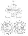
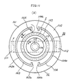
- Fig. 2(a)-(c) Japanese laid-open Patent Publication (unexamined) No.57-3327.
- Fig. 2 (a) is a side view showing an example of arrangement of electrodes in such prior vacuum interrupter
- Fig. 2 (b) is a plan view in the direction of the arrow b-b
- Fig. 2 (c) is a plan view in the direction of the arrow c-c.
- reference numerals (50), (60) designate bridge conductors respectively fixed on the ends of the bridge conductors (5), (6). These bridge conductors (5), (6) are rectangular and projecting parts (51), (52), (61), (62) are respectively formed on both ends thereof. Numerals (30), (40) disignate a pair of electrodes connected electrically to each bridge conductor (50), (60) on their outer peripheral back sides respectively.
- circular arc-shaped grooves (33), (34), (43), (44) serving as high resistance areas are formed on each electrode (30), (40) by cutting at required distances, thus circular arc-shaped electrode parts (31), (32) and (41), (42) serving as outside parts of the electrodes partitioned by these grooves (33), (34) and (43), (44) are formed.
- Said bridge conductor (50) is so arranged as to cross the grooves (43), (44), and the projecting parts (51), (52) and (61), (62) are electrically and mechanically connected to substantially central parts of said circular arc-shaped electrode parts (31), (32) and (41), (41).
- Gaps between said bridge conductors (50), (60) and the electrodes (30), (40) are desired to be as small as possible, but it is necessary that the gaps are in a range in which the electrodes (30), (40) do not come in contact with the bridge conductors (50), (60) when the electrodes are butted to each other bringing about elastic deformation due to a mechanical force applied.
- the aforesaid electrode (30) and the bridge conductor (50) are respectively of the same configuration as the electrode (40) and the bridge conductor (60), but the electrode (40) and the bridgre conductor (60) are so arranged as to face to the electrode (30) and the brdige conductor (50) by 90° respectively being deviated by 90° therefrom.
- the (51) ⁇ (31) ⁇ B ⁇ A is a loop formed by the electrode itself, the loop is near the point A and a strong axial magnetic field is generated.
- the current i passes from the point A' of the other electrode (40) to the conductive rod (6) by way of a gap C between the grooves (43), (44) of the electrode (40), the circular arc-shaped electrode part (41), the projecting part (61) and the bridge conductor (60). That is, one turn is further formed by a current loop A' ⁇ C ⁇ (41) ⁇ (61) ⁇ (60) ⁇ (6) is further formed, and a magnetic field of the same axial direction as the foregoing loop is generated.
- a strong combined magnetic flux in the axial direction acts in parallel to the arc A-A' as indicated by the arrow ⁇ in Fig. 2(a), effectively preventing emission and diffusion of ionized metals from the arc to outside, acquiring a sufficient amount of plasma particles and stabilizing the arc.
- an electro-magnetic repulsive force is generated at the contact points due to concentration of the current and acts to separate the electrodes 30, 40, but since the current direction from the projecting part 51 to the tap B in the electrode 30 is same as that from the gap C to the projecting part 61 in the other electrode 40, the circular arc-shaped electrode parts 31, 41 are strongly attracted to each other.
- the electrode contact force applied to said electrodes 30, 40 can be greatly reduced by means of the operation mechanism not shown, and the operation mechanism can be small-sized and light-weight.
- DE-A-3416368 discloses a vacuum interrupter generally similar to that shown in figure 2 but additionally provided with rectilinear slots in the electrode extending radially inwards from the circular arc-shaped grooves serving as high resistance areas, in order to direct and concentrate the current flow path and enhance the magnetic field generated, while reducing eddy currents.
- the object of the invention is to provide electrode structures for vacuum interrupters, in which the interrupting performance is still further improved relative to the prior art.
- a vacuum interrupter for opening and closing a current passage by a pair of electrodes which are incorporated in a vacuum container, connectable to and separable from each other and respectively mounted on conductive rods, wherein at least one of said pair of electrodes is provided with first high resistance areas formed passing through from a back side towards a contact surface thereof at specified distances from a peripheral edge of the electrode and facing each other, and second high resistance areas extending from ends of the first high resistance areas towards the centre of said electrode and not connected to each other, and wherein outside parts of the electrode between the first high resistance areas and said peripheral edge are electrically connected to said conductive rod on said back side of the electrode by way of a bridge conductor (50) arranged over the first high resistance areas, characterised by annular third high resistance areas (59) formed from the first high resistance areas inside the electrode to said peripheral edge of the electrode.
- a vacuum interrupter for opening and closing a current passage by a pair of electrodes which are incorporated in a vacuum container, connectable to and separable from each other and respectively mounted on conductive rods, wherein at least one of said pair of electrodes comprises at least one first high resistance area formed passing through from a facing surface to a back side thereof at specified distances from a peripheral edge of the electrode and facing each other, and a bridge conductor arranged over the first high resistance areas and electrically connecting outside parts of the electrode between the first high resistance areas and said peripheral edge to said conductive rod on said back side of the electrode, characterised by a second high resistance area formed inside the first high resistance area or areas of said electrode and passing through said electrode connecting an annular high resistance area of which the outer diameter is D1 on the back side of the electrode to an annular high resistance area (107b) of which the outer diameter is D2 in the facing sides of the electrode where D1>D2, a contact (113, 133) projecting in the form of a ring and of
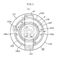
- Figure 3 (a) is a side view showing an electrode structure of a vacuum interrupter
- Fig. 3 (b) is a plan view in the direction of the arrow b-b in Figure 3
- Figure 3 (b) is a plan view in the direction of the arrow b-b in Fig. 3 (a)
- Fig. 3 (c) is a plan view in the direction of the arrow c-c in Fig. 3 (a).
- reference numberals 33, 34, 43, 44 denote high resistance areas formed on each electrode 30, 40 passing through from the contact surface to the back side thereof at specified distances from peripheral edges of the electrode 30, 40, and the high resistance areas are arranged symmetrical to the center of each electrode forming a pair of grooves not connected to each other.
- Numerals 35 to 38, 45 to 48 denote second high resistance areas extending from both ends of the first high resistance areas 33, 34, 43, 44 towards the center of each electrode 30, 40, and the second high resistance areas are linear grooves formed substantially perpendicular to bridge conductors 50, 60.
- Each electrode 30, 40 is partitioned by the first and second high resistance areas 33 to 38, 45 to 48, thereby current paths 53, 54, 55, 56 towards outside parts 31, 32, 41, 42 of the electrodes 30, 40 and center parts thereof are formed.
- the width of each current path 53 to 56 is narrower than that of the bridge conductors 50, 60.
- the bridge conductors 50, 60 are arranged over the first high resistance areas 33, 34, 41, 42 to electrically and mechanically connect the outside parts 31, 32, 41, 42 to conductive rods 5, 6.
- the electrode 30 and the bridge conductor 50 are of the same configuration as the electrode 40 and the bridge conductor 50 respectively, but the electrode 40 and the bridge conductor 60 are so arranged as to face to the electrode 30 and the bridge conductor 50 respectively being deviated by 90° therefrom.
- an arc is formed between the electrodes 30, 40.
- a current i passes from the conductive rod 5 towards the conductive rod 6 and the arc is formed between a point A of one electrode 30 and a point A' of the other electrode 40, the current i passes from the conductive rod 5 to the arc point A by way of the bridge conductor 50, the projecting part 51, the outside part 31 and the current passage 53. That is, a complete one turn is formed by a current loop 50 ⁇ 51 ⁇ 31 ⁇ 53 ⁇ A, and wherein since the 51 ⁇ 31 ⁇ 53 ⁇ A is a loop formed by the electrode itself and situated near the arc point A, a strong axial magnetic field is generated.
- the current i passes from the other point A' of the electrode 40 to the conductive rod 6 by way of the current passage 55, the outside part 41, the projecting part 61 and the bridge conductor 60. That is, a complete one turn is formed by the current loop A' ⁇ 55 ⁇ 41 ⁇ 61 ⁇ 60 ⁇ 6 and the same axial magnetic field as the foregoing current loop is formed.
- a strong combined axial magnetic flux acts in parallel to the arc A-A' indicated by the arrow ⁇ in Fig. 3 (a), emission and diffusion of ionized metals to outside are effectively prevented and the arc is stabilized by acquiring a sufficient amount of plasma particles.
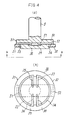
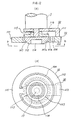
- Fig. 4 a, b shows a thin electrode structure attained by interposing a reinforcing member 57 between the bridge conductor 50 and the electrode, considering that electrode materials of high conductivity such as copper, silver used in general have disadvantages in view of mechanical strength and cost saving.
- An inside part 39 of the electrode 30 slightly projects to prevent application of mechanical force to the outside parts 31, 32 of the electrode and arm parts of the bridge conductor 50 when performing opening and closing.
- a material, such as stainless steel, of less conductivity than the electrode material is preferably used as the reinforcing member 57. It is also satisfactory to form the inside part 39 of the electrode 30 of an electrode material resistant to welding the high pressure, while forming the outside parts 31, 32 of ordinary copper.
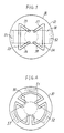
- the axial magnetic field can be generated even when the first high resistance areas 33, 34 are formed linear as in Fig. 5 instead of being circular arc-shaped. It is further preferable that, as shown in Fig. 6, the bridge conductor 50 is divided into three parts and the first high resistance areas are arranged to cross them, thereby increasing the area of generating the axial magnetic field. In this case, the electrodes facing each other are desired to be deviated by 60° from each other. It is further preferable that the bridge conductor is divided into more than three parts and the first high resistance areas are arranged to cross them.
- the high resistance areas in the electrodes described above can be formed by filling the groove 33 38, 43 48 with a high resistance material.
- Fig. 7 (a) is a side view showing an electrode structure of a vacuum interrupter in accordance with an embodiment of the present invention
- Fig. 7, (b) is a plan view in the direction of the arrow b-b
- Fig. 7 (c) is a plan view in the direction of the arrow c-c in fig. 7 (a).
- reference numerals 33, 34, 43, 44 denote grooves for the first high resistance areas in the same manner as in Fig.
- grooves do not pass through the contact surfaces of the electrodes 30, 40, and the grooves have a certain depth from the back sides of the electrodes 30, 40 towards the contact surfaces and are formed at a certain distance from the peripheral edges of the electrodes 30, 40.
- reference numerals 35 to 38, 45 to 48 denote the second high resistance areas, but they do not pass through from the contact surfaces of the electrodes 30, 40 toward the backs, and the grooves have a certain depth from the backs of the electrodes 30, 40 towards the contact surfaces.
- Numerals 59, 69 denote circular third high resistance areas formed inside the electrodes extending from the first high resistance areas 33, 34, 43, 44 towards the electrode peripheral edges and they are grooves in this embodiment. The arrangement of the grooves is also shown in Fig. 8.
- an arc A is formed between the electrodes 30, 40.
- This arc A is formed on all surfaces of the electrodes 30, 40 when the arc current is very large.
- the current i to passing from the conductive rod 5 towards the conductive rod 6 first passes from said conductive rod 5 being divided into two currents passing reversely to each other as shown in Fig. 7 (a), then passes reversely to each other as shown in Fig. 7 (a), then passes through the circular arc-shaped electrode parts 31, 32 by way of the projecting parts 52, 53 as shown in Fig.
- the current i coming from the contact surfaces passes through the current passages 55 and 56 being divided into two currents, then passes through the circular arc-shaped electrode parts 41, 42 in the reverse direction, and after passing through the projecting parts 61 and 62, reaches the conductive rod 6 by way of the bridge conductor 60.
- the axial magnetic fields generated by each loop are in reverse directions to one another as shown in Fig. 7 (b), (c) and the magnetic fields in the center part of the electrode axis are mutually offset.
- a residual magnetic flux affecting the extinction of ionized metals in the arc can be reduced.
- a strong axial magnetic field acts on almost all over the contact surfaces of the electrodes parallel to the arc, thereby the arc is stably and uniformly distributed.
- the high resistance areas 33 to 38, 43 to 48, 59, 69 are not exposed on the contact with the arc, local melting due to arc energy concentration can be effectively prevented.
- FIG. 8 (a), (b), A further embodiment of the present invention is shown in Fig. 8 (a), (b), wherein a thin electrode structure is attained by interposing a reinforcing member 57 between the bridge conductor 50 and the electrode 30, because electrode materials of high conductivity such as copper or silver used in general have disadvantages in view of mechanical strength and cost saving.
- An inside part 39 of the electrode 30 projects to prevent application of mechanical force to the outside parts 31, 32 of the electrode and arm parts of the bridge conductor 50 when performing opening and closing.
- a material, such as stainless steel, of less conductivity than the electrode material is preferably used as the reinforcing member 57. It is also satisfactory to form the inside part 39 of the electrode 30 of an electrode material resistant to welding and high pressure, while forming the outside parts 31, 32 of ordinary copper.
- the axial magnetic field can be generated even when the first high resistance areas 33, 34 are formed linear as in the embodiment of Fig. 9 instead of being circular arc-shaped.
- the bridge conductor 50 is divided into three parts and the first high resistance areas are arranged to cross them, thereby increasing the area of generating the axial magnetic field.
- the electrodes facing to each other are desired to be deviated by 60° from each other.
- the bridge conductor is divided into more than three parts and the first high resistance areas are arranged to cross them.
- the high resistance areas in the embodiments described above can be formed by impregnating a high resistance material in the groove 33 38, 43 48.
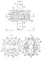
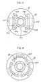
- Fig. 11 (a) is a side view showing an electrode structure of a vacuum interrupter in accordance with the present invention
- Fig. 11 (b) is a plan view in the direction of the arrow b-b in fig. 11 (a)
- Fig. 11 (c) is a plan view in the direction of the arrow c-c in Fig. 11 (a)
- Fig. 11 (d) is an explanatory sectional view showing one electrode in fig. 11 (a).
- reference numerals 103, 104, 123, 124 denote the first high resistance areas formed on each electrode 10, 20 facing one another, passing through from the facing surfaces to the back and keeping certain distances from the peripheral edges of the electrodes 10, 20, e.g., at about 20% of the diameter.
- the first high resistance areas are formed of grooves consisting of a pair of circular arc-shaped parts 103a, 104a, 123a, 124a arranged substantially symmetrical to the center of each electrode and not connected one another, and linear parts 103b, 103c, 104b, 104c, 123b, 123c, 124b, 124c extending from both ends of the circular arc towards the center of each electrode substantially perpendicular to the bridge conductors 50, 60 and not connected to one another.
- Numerals 107, 108 denote second high resistance areas provided inside the first high resistance areas 103, 104, 123, 124, and, as shown in Fig.
- these second high resistance areas pass through the electrodes 10, 20 connecting an annular high resistance area of which the outer diameter is D1 on the electrode back sides, to an annular high resistance area of which the outer diameter is D2 (where D1>D2) on the electrode facing sides.
- parallel annular parts 107a, 108a are formed on the electrode backs, while inclined annular parts 107b, 108b are formed on the electrode facing sides towards the center of the electrode in continuation to the parallel annular parts 107a, 108a.
- the second high resistance areas are actually formed of annular grooves coaxial with the first high resistance areas 103, 104, 123, 124.
- Numerals 113, 133 denote contacts each projecting in a form of a ring of which the inner diameter is D3, i.e. with central recesses 114, 134 of diameter D3.
- the electrodes 5, 6 are connected to the backs of the contacts 113, 134 by way of cylindrical conductive members 115, 135 with outer diameter D4 for electrical connection to the outside of the vacuum container. Since there is the relation of D3 > D4 between this outer diameter D4 of the conductive members 115, 135 and the inner diameter D3 of the contacts 113, 133, the contacts 113, 133 come in contact with each other outside the diameter D4.
- these contacts 113, 133 are made of an alloy of low melting point material such as bismuth and copper of which the mechanical strength is not high, and therefore in order to prevent the electrodes 10, 20 from deformation and breakage when they are opened and closed, reinforcing members 116, 136 of low conductivity and high mechanical strength as compared with copper, etc. are fixed to the back sides of the contacts 113, 133. Since the electrodes 10, 20 are disposed on the outer peripheries of the contacts 113, 133, the electrodes are insulated from the contacts 113, 133 with high insulation material as compared with the spacing portion or copper material forming the second high resistance areas 107, 108.
- Each electrode 10, 20 is partitioned by the first high resistance areas 103, 104, 123, 124 respectively.
- the bridge conductors 50, 60 are respectively arranged on the backs of the electrodes over the first high resistance areas 103, 104, 123, 124 so that the electrode outside parts 10, 20 and 131, 132 are electrically and mechanically connected to the conductive rods 5, 6.
- the electrodes 10, 20 are formed of an alloy of copper and chromium.
- the electrode 30 and the bridge conductor 50 are of the same configuration as the electrode 40 and the bridge conductor 50 respectively in this embodiment, but the electrode 40 and the bridge conductor 60 are so arranged as to face to the electrode 30 and the bridge conductor 50 respectively being deviated by 90° therefrom. This is because a magnetic field formed by the current passing through one electrode is in the same direction as a magnetic field formed by the current passing through the other electrode.
- the vacuum interrupter arranged as above described performs the following operation.
- the current passage is formed by the conductive rod 5, the conductive member 115, the contacts 113, 133, the conductive member 135 and the conductive rod 6 in that order.
- the outer diameter D4 of the conductive members 115, 135 and the inner diameter D3 of the contacts 113, 133 are in the relation D3 ⁇ D4, the current does not pass rectilinearly but is curved between the conductive members 115, 135 and the contacts 113, 133, thereby an arc formed after opening the electrodes being easily transferred.
- the current passes as indicated by the broken line in Fig. 11 (a) and an arc is formed between a point A of the contact 113 and a point A' of the contact 133. Since a force extending the arc from the surfaces of the contacts 113, 133 outward is applied to the arc, the arc is transferred across the second high resistance areas 107 to ignite between points B, B' on the surfaces of the electrodes 10, 20.
- the current i passes from the conductive rod 5 to the point B by way of the bridge conductor 50, projecting part 111, outside part 10 of the electrode and through between the linear parts 103c, 104c in the first high resistance areas.
- the current i further passes from the point B' to the bridge conductor 60 through between the linear parts 123b, 124b in the first high resistance areas and by way of the outside part 131 of the electrode and projecting part 141.
- each one turn is formed by the current loop 50 ⁇ 111 ⁇ 101 ⁇ B and B' ⁇ 131 ⁇ 141 ⁇ 60, and an axial magnetic field is generated.
- an arc is stably and uniformly distributed on the surfaces of the electrodes, enabling interruption of large currents thereby.
- Fig. 12 (a), (b) are a sectional view and a plan view in the direction of the arrow b-b of a portion near one electrode of a vacuum interrupter in accordance with a yet further embodiment, each first high resistance area is formed into one circular arc and the bridge conductor 50 is transformed according to such configuration of the first high resistance areas.
- the applied current does not pass through the electrode 10 and the bridge conductor 50 and Joule's heat is not generated, either, in this embodiment.
- the electrode 10 can be connected to the bridge conductor 50 at only one point in the projecting part 111.
- the current passing outside part of the first high resistance areas 104 is increased more, than the foregoing embodiment, and it is possible to generate a stronger axial magnetic field resulting in improvement of the interruption performance.
- Fig. 12 (a), (b) Although only one electrode 30 and one bridge conductor 50 are shown in Fig. 12 (a), (b), it is further possible to have a structure in which both or either of the facing electrodes and the bridge 2onductors is arranged as shown in Fig. 12 (a), (b).
- the axial magnetic field can be generated even when the first high resistance areas 33, 34 are formed linear as in fig. 13 instead of being circular arc-shaped.
- the bridge conductor 50 is divided into three parts and the first high resistance areas are arranged to cross them, thereby increasing the area of generating the axial magnetic field.
- the electrodes facing each other are desired to be deviated by 60° from each other considering the direction of the magnetic field.
- the bridge conductor is divided into more than three parts and the first high resistance areas are arranged to cross them.
- the high resistance areas in the embodiments described above can be formed by filling the grooves with a high resistance material.
- it is satisfactory if the first high resistance areas have no linear parts perpendicular to the bridge conductors and extending towards the center of each electrode.
Landscapes
- High-Tension Arc-Extinguishing Switches Without Spraying Means (AREA)
Claims (11)
- Vakuum-Leistungsschalter zum Einschalten und Ausschalten eines Stromdurchganges durch ein Paar von Elektroden (10, 20), die in einen Vakuumbehälter eingebaut, miteinander verbindbar und voneinander trennbar und jeweils an leitfähigen Stangen angebracht sind, wobei wenigstens die eine Elektrode des Paars von Elektroden folgendes aufweist: erste Bereiche (33, 34) mit hohem Widerstand, die so ausgebildet sind, daß sie von einer Rückseite in Richtung zu einer Kontaktfläche davon in bestimmten Abständen von einem Umfangsrand der Elektrode hindurchgehen und einander Zugewandt sind, sowie zweite Bereiche (35-38) mit hohem Widerstand, die sich von den Enden der ersten Bereiche mit hohem Widerstand in Richtung zum Mittelpunkt der Elektrode erstrecken und nicht miteinander verbunden sind, und wobei äußere Teile der Elektrode zwischen den ersten Bereichen mit hohem Widerstand und dem Umfangsrand mit der leitfähigen Stange an der Rückseite der Elektrode über einen Brückenleiter (50) elektrisch verbunden sind, der über den ersten Bereichen mit hohem Widerstand angeordnet ist,
gekennzeichnet durch
ringförmige dritte Bereiche (59) mit hohem Widerstand, die ausgehend von den ersten Bereichen mit hohem Widerstand innerhalb der Elektrode zu dem Umfangsrand der Elektrode hin gebildet sind. - Vakuum-Leistungsschalter nach Anspruch 1, wobei die ersten Bereiche mit hohem Widerstand kreisbogenförmige Bereiche mit hohem Widerstand sind, die im wesentlichen symmetrisch zu dem Mittelpunkt der Elektrode angeordnet und nicht miteinander verbunden sind.
- Vakuum-Leistungsschalter nach Anspruch 1 oder 2, wobei die ersten, zweiten und dritten Bereiche mit hohem Widerstand jeweils hohle Nuten sind.
- Vakuum-Leistungsschalter nach Anspruch 1, 2 oder 3, wobei die inneren und äußeren Teile der Elektrode jeweils aus verschiedenen Elektrodenmaterialien gebildet sind.
- Vakuum-Leistungsschalter nach Anspruch 1, 2, 3 oder 4, wobei die zweiten Bereiche mit hohem Widerstand so angeordnet sind, daß sie einander näher sind als die Breite des Brückenleiters (50) ausmacht.
- Vakuum-Leistungsschalter zum Einschalten und Ausschalten eines Stromdurchganges durch ein Paar von Elektroden (10, 20), die in einen Vakuumbehälter eingebaut, miteinander verbindbar und voneinander trennbar und jeweils an leitfähigen Stangen (5, 6) angebracht sind, wobei wenigstens die eine Elektrode des Paars von Elektroden folgendes aufweist: wenigstens einen ersten Bereich (103, 104, 123, 124) mit hohem Widerstand, der so ausgebildet ist, daß er von einer zugewandten Fläche zu einer Rückseite davon in bestimmten Abständen von einem Umfangsrand der Elektrode hindurchgeht, wobei die ersten Bereiche einander gegenüberliegen, und einen Brückenleiter (50), der über den ersten Bereichen mit hohem Widerstand angeordnet ist und äußere Teile der Elektrode zwischen den ersten Bereichen mit hohem Widerstand und dem Umfangsrand mit der leitfähigen Stange (5, 6) an der Rückseite der Elektrode elektrisch verbindet,
gekennzeichnet durch
einen zweiten Bereich (107, 108) mit hohem Widerstand, der innerhalb des ersten Bereichs oder der ersten Bereiche mit hohem Widerstand der Elektrode gebildet ist und der durch die Elektrode hindurchgeht und einen ringförmigen Bereich (107a) mit hohem Widerstand, dessen Außendurchmesser D₁ an der Rückseite der Elektrode ist, mit einem ringförmigen Bereich (107b) mit hohem Widerstand, dessen Außendurchmesser D₂ in den einander zugewandten Seiten der Elektrode ist, verbindet, wobei D₁ > D₂ gilt und wobei ein Kontakt (113, 133) in Form eines Rings vorsteht, dessen Innendurchmesser D₃ ist, und durch ein zylindrisches leitfähiges Element, dessen Durchmesser D₄ ist, das den Kontakt mit der leitfähigen Stange (5, 6) verbindet, wobei D₃ > D₄ gilt. - Vakuum-Leistungsschalter nach Anspruch 6, wobei die ersten Bereiche mit hohem Widerstand folgendes aufweisen: kreisbogenförmige Teile mit im wesentlichen gleichen Durchmessern, die um den Mittelpunkt der Elektrode herum in im wesentlichen gleichen Abständen angeordnet und nicht miteinander verbunden sind, und geradlinige Teile, die sich von den Enden der kreisbogenförmigen Teile in Richtung zum Mittelpunkt der Elektrode hin erstrecken und nicht miteinander verbunden sind.
- Vakuum-Leistungsschalter nach Anspruch 6 oder 7, wobei die Bereiche mit hohem Widerstand hohle Nuten sind.
- Vakuum-Leistungsschalter nach einem der Ansprüche 1 bis 8, wobei ein Verstärkungsmaterial (57, 116, 136) mit geringerer Leitfähigkeit als das Material der Elektrode zwischen den Brückenleiter und die Elektrode eingefügt ist.
- Vakuum-Leistungsschalter nach Anspruch 9, wobei der Durchmesser des Verstärkungsmaterials kleiner als die Breite der Brücke ist.
- Vakuum-Leistungsschalter nach einem der Ansprüche 1 bis 10, wobei beide Elektroden des Paars von Elektroden mit im wesentlichen gleicher Konfiguration geformt und die Elektroden einander zugewandt sind, wobei ihre Winkel voneinander abweichen, so daß ein Magnetfeld, das von einem durch die eine Elektrode hindurchgehenden Strom erzeugt wird, in der gleichen Richtung verläuft wie das Magnetfeld, das von einem durch die andere Elektrode hindurchgehenden Strom erzeugt wird.
Applications Claiming Priority (6)
| Application Number | Priority Date | Filing Date | Title |
|---|---|---|---|
| JP253962/85 | 1985-11-12 | ||
| JP253961/85 | 1985-11-12 | ||
| JP25396185A JPS62113328A (ja) | 1985-11-12 | 1985-11-12 | 真空しや断器 |
| JP25396285A JPH0670889B2 (ja) | 1985-11-12 | 1985-11-12 | 真空しや断器 |
| JP195966/86 | 1986-08-21 | ||
| JP19596686A JPH0693341B2 (ja) | 1986-08-21 | 1986-08-21 | 真空しや断器 |
Publications (2)
| Publication Number | Publication Date |
|---|---|
| EP0245513A1 EP0245513A1 (de) | 1987-11-19 |
| EP0245513B1 true EP0245513B1 (de) | 1993-09-29 |
Family
ID=27327173
Family Applications (1)
| Application Number | Title | Priority Date | Filing Date |
|---|---|---|---|
| EP86906924A Expired - Lifetime EP0245513B1 (de) | 1985-11-12 | 1986-11-12 | Vakuumschalter |
Country Status (4)
| Country | Link |
|---|---|
| US (1) | US4855547A (de) |
| EP (1) | EP0245513B1 (de) |
| DE (1) | DE3689122T2 (de) |
| WO (1) | WO1987003136A1 (de) |
Families Citing this family (5)
| Publication number | Priority date | Publication date | Assignee | Title |
|---|---|---|---|---|
| US5387771A (en) * | 1993-04-08 | 1995-02-07 | Joslyn Hi-Voltage Corporation | Axial magnetic field high voltage vacuum interrupter |
| DE19534398A1 (de) * | 1995-09-16 | 1997-03-20 | Abb Patent Gmbh | Kontaktanordnung für eine Vakuumschaltkammer |
| DE19716278A1 (de) * | 1997-04-18 | 1998-10-22 | Abb Patent Gmbh | Vakuumschaltgerät |
| DE19809305A1 (de) * | 1998-03-05 | 1999-09-09 | Abb Patent Gmbh | Kontaktstückanordnung für eine Vakuumkammer |
| CN107093535B (zh) * | 2017-06-06 | 2020-02-11 | 西安交通大学 | 一种高额定电流纵向磁场真空灭弧室触头结构 |
Family Cites Families (8)
| Publication number | Priority date | Publication date | Assignee | Title |
|---|---|---|---|---|
| US3327081A (en) * | 1964-11-25 | 1967-06-20 | Allis Chalmers Mfg Co | Contact with high resistance material insert |
| JPS58810B2 (ja) * | 1976-12-06 | 1983-01-08 | 株式会社日立製作所 | 真空しや断器 |
| DE3173171D1 (en) * | 1980-12-22 | 1986-01-23 | Mitsubishi Electric Corp | Vacuum interrupter |
| JPS58100325A (ja) * | 1981-12-09 | 1983-06-15 | 三菱電機株式会社 | 真空しや断器 |
| DE3401497A1 (de) * | 1982-07-22 | 1984-08-09 | Ernst Prof. Dr.techn.habil. 1000 Berlin Slamecka | Vakuumschalter-kontaktanordnung |
| DE3235298A1 (de) * | 1982-09-21 | 1984-03-22 | Siemens AG, 1000 Berlin und 8000 München | Vakuumschaltroehre mit ringteil und diametralem steg der schaltstuecke |
| DE3416368C2 (de) * | 1984-04-30 | 1986-07-17 | Ernst Prof. Dr.techn.habil. 1000 Berlin Slamecka | Vakuumschalter-Kontaktanordnung |
| JPS61195528A (ja) * | 1985-02-22 | 1986-08-29 | 三菱電機株式会社 | 真空しや断器の電極構造 |
-
1986
- 1986-11-12 EP EP86906924A patent/EP0245513B1/de not_active Expired - Lifetime
- 1986-11-12 DE DE86906924T patent/DE3689122T2/de not_active Expired - Fee Related
- 1986-11-12 WO PCT/JP1986/000576 patent/WO1987003136A1/en not_active Ceased
- 1986-11-12 US US07/069,555 patent/US4855547A/en not_active Expired - Fee Related
Also Published As
| Publication number | Publication date |
|---|---|
| WO1987003136A1 (en) | 1987-05-21 |
| DE3689122T2 (de) | 1994-05-05 |
| EP0245513A1 (de) | 1987-11-19 |
| DE3689122D1 (de) | 1993-11-04 |
| US4855547A (en) | 1989-08-08 |
Similar Documents
| Publication | Publication Date | Title |
|---|---|---|
| US3946179A (en) | Vacuum interrupter | |
| KR100295905B1 (ko) | 진공인터럽터용전극구조체 | |
| CA1077547A (en) | Vacuum type circuit interrupter with a contact having integral axial magnetic field means | |
| US5438174A (en) | Vacuum interrupter with a radial magnetic field | |
| JP2002184273A (ja) | 真空遮断機用真空インタラプター | |
| CA1118475A (en) | Vacuum-type circuit interrupter with an improved contact with axial magnetic field coil | |
| JPH027318A (ja) | バキュームインターラプタ | |
| CA1224233A (en) | Vacuum interrupter | |
| JPS62103928A (ja) | 真空しや断器 | |
| US3764764A (en) | Vacuum circuit breaker | |
| US4553002A (en) | Axial magnetic field vacuum-type circuit interrupter | |
| KR920006060B1 (ko) | 진공스위치관 | |
| US3935406A (en) | Vacuum interrupter | |
| EP0245513B1 (de) | Vakuumschalter | |
| EP0052371B1 (de) | Vakuumschalter | |
| KR880002576B1 (ko) | 진공 차단기 | |
| JPH0112355Y2 (de) | ||
| JP3577740B2 (ja) | 真空バルブ | |
| JPH0670889B2 (ja) | 真空しや断器 | |
| JP3231595B2 (ja) | 真空バルブ | |
| JPH03272530A (ja) | 真空遮断器用真空バルブ | |
| JP3431487B2 (ja) | 真空バルブ | |
| JPS6313633Y2 (de) | ||
| JPH0693341B2 (ja) | 真空しや断器 | |
| JPH11149855A (ja) | 回路遮断器 |
Legal Events
| Date | Code | Title | Description |
|---|---|---|---|
| PUAI | Public reference made under article 153(3) epc to a published international application that has entered the european phase |
Free format text: ORIGINAL CODE: 0009012 |
|
| 17P | Request for examination filed |
Effective date: 19870630 |
|
| AK | Designated contracting states |
Kind code of ref document: A1 Designated state(s): DE GB |
|
| 17Q | First examination report despatched |
Effective date: 19910313 |
|
| GRAA | (expected) grant |
Free format text: ORIGINAL CODE: 0009210 |
|
| AK | Designated contracting states |
Kind code of ref document: B1 Designated state(s): DE GB |
|
| REF | Corresponds to: |
Ref document number: 3689122 Country of ref document: DE Date of ref document: 19931104 |
|
| REG | Reference to a national code |
Ref country code: GB Ref legal event code: 727A |
|
| REG | Reference to a national code |
Ref country code: GB Ref legal event code: 727B |
|
| REG | Reference to a national code |
Ref country code: GB Ref legal event code: SP |
|
| PLBE | No opposition filed within time limit |
Free format text: ORIGINAL CODE: 0009261 |
|
| STAA | Information on the status of an ep patent application or granted ep patent |
Free format text: STATUS: NO OPPOSITION FILED WITHIN TIME LIMIT |
|
| 26N | No opposition filed | ||
| REG | Reference to a national code |
Ref country code: GB Ref legal event code: 746 Effective date: 19951026 |
|
| PGFP | Annual fee paid to national office [announced via postgrant information from national office to epo] |
Ref country code: GB Payment date: 19981113 Year of fee payment: 13 |
|
| PGFP | Annual fee paid to national office [announced via postgrant information from national office to epo] |
Ref country code: DE Payment date: 19981120 Year of fee payment: 13 |
|
| PG25 | Lapsed in a contracting state [announced via postgrant information from national office to epo] |
Ref country code: GB Free format text: LAPSE BECAUSE OF NON-PAYMENT OF DUE FEES Effective date: 19991112 |
|
| GBPC | Gb: european patent ceased through non-payment of renewal fee |
Effective date: 19991112 |
|
| PG25 | Lapsed in a contracting state [announced via postgrant information from national office to epo] |
Ref country code: DE Free format text: LAPSE BECAUSE OF NON-PAYMENT OF DUE FEES Effective date: 20000901 |