EP0244571A2 - RF-Synthezierer mit niedrigem Phasenrauschen - Google Patents
RF-Synthezierer mit niedrigem Phasenrauschen Download PDFInfo
- Publication number
- EP0244571A2 EP0244571A2 EP87102161A EP87102161A EP0244571A2 EP 0244571 A2 EP0244571 A2 EP 0244571A2 EP 87102161 A EP87102161 A EP 87102161A EP 87102161 A EP87102161 A EP 87102161A EP 0244571 A2 EP0244571 A2 EP 0244571A2
- Authority
- EP
- European Patent Office
- Prior art keywords
- frequency
- signal
- output
- mhz
- loop
- Prior art date
- Legal status (The legal status is an assumption and is not a legal conclusion. Google has not performed a legal analysis and makes no representation as to the accuracy of the status listed.)
- Granted
Links
- 230000001360 synchronised effect Effects 0.000 claims 2
- 238000000034 method Methods 0.000 description 4
- 238000010586 diagram Methods 0.000 description 3
- 239000013078 crystal Substances 0.000 description 2
- 230000000694 effects Effects 0.000 description 1
- 230000003595 spectral effect Effects 0.000 description 1
- 238000010897 surface acoustic wave method Methods 0.000 description 1
Images

Classifications
-
- H—ELECTRICITY
- H03—ELECTRONIC CIRCUITRY
- H03L—AUTOMATIC CONTROL, STARTING, SYNCHRONISATION OR STABILISATION OF GENERATORS OF ELECTRONIC OSCILLATIONS OR PULSES
- H03L7/00—Automatic control of frequency or phase; Synchronisation
- H03L7/06—Automatic control of frequency or phase; Synchronisation using a reference signal applied to a frequency- or phase-locked loop
- H03L7/16—Indirect frequency synthesis, i.e. generating a desired one of a number of predetermined frequencies using a frequency- or phase-locked loop
- H03L7/22—Indirect frequency synthesis, i.e. generating a desired one of a number of predetermined frequencies using a frequency- or phase-locked loop using more than one loop
- H03L7/23—Indirect frequency synthesis, i.e. generating a desired one of a number of predetermined frequencies using a frequency- or phase-locked loop using more than one loop with pulse counters or frequency dividers
Definitions
- the invention relates generally to a low noise RF frequency synthesizer, and in particular to a quiet, inexpensive IF reference loop for an RF synthesizer which gives very low phase noise levels at a relatively low cost.
- a well-known tradeoff in synthesizer design is between frequency resolution on one hand and phase noise or spectral purity on the other.
- the problem arises because the noise content of a signal increases somewhat linearly as the bandwidth of the signal increases.
- increasing the frequency resolution results in an output signal with higher phase noise.
- synthesizers have used a series of phase-locked loops generating successively narrower frequency ranges and equivalent bandwidths. In order to achieve 1.0 Hz resolution over 1000 to 1500 MHz, five or six separate loops have typically been required. The frequencies are generated by multiplying a reference frequency through a series of multipliers and using summing loops for each frequency range. One technique uses a fractional-N summing loop for the final high resolution loop. The main disadvantage of these synthesizers has been that many loops are required to provide both the desired low noise signal, high resolution and wide frequency coverage at the same time. This increases the cost and complexity of the synthesizer.
- An object of the invention is to provide a relatively low cost synthesizer that produces a low noise, high resolution signal over a wide frequency range.
- Another object of the invention is to provide a synthesizer that produces the desired output signal using fewer phase-locked loop circuits than currently known devices.
- a further object of the invention is to provide a synthesizer whose output signal contains the prime factors up to five in its divisor, so that the synthesizer's output signal can be multiplied by any of those factors without producing a fractional frequency result.
- a relatively low cost synthesizer achieves 1.0 Hz resolution over a 1000 to 1500 MHz frequency range with a low phase noise output signal using only three phase-locked loops.
- the base RF signal 980 to 1520 MHz in 20 MHz steps is generated by one loop, while the high resolution IF signal is generated by a fractional-N loop.
- the RF and IF signals are combined in a third phase-locked loop, the output sum loop, to produce the output signal.
- a programmable variable divider divides the IF output frequency, achieving coverage over the necessary frequency range by changing the divide number.
- the fractional-N circuit thus only has to fill in the fine steps between the divide numbers, with the largest bandwidth requirement being the range between the two lowest divide numbers. This reduces the effect of the noise from the IF reference loop because the coverage obtained by increasing the divide number reduces noise in contrast to the other techniques for increasing frequency coverage which increase noise.
- Another aspect of the invention is the use of a reference frequency in the fractional-N loop that has each of the factors 2, 3, and 5 in its divisor. This is accomplished by substituting a divide-by-96 circuit where a divide-by-100 would normally be used. The result is that the output signal of the synthesizer can be multiplied by any of these factors without producing a fractional frequency.
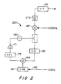
- the synthesizer includes three phase-locked loops and a reference frequency section.
- the RF frequencies are directly or indirectly generated from a 100 MHz crystal oscillator in the timebase section 141.
- RF reference loop 121 generates an RF signal that can step from 980 MHz to 1520 MHz in 20 MHz steps using the reference frequencies from timebase section 141.
- IF reference loop 161 provides the high resolution fine frequency steps, generating a 10 MHz to 20 MHz signal with 1.0 Hz steps.
- the RF and IF signals are combined in the output sum loop 193, yielding the output signal of 980 MHz to 1520 MHz with 1.0 Hz resolution.
- Timebase 141 provides reference and mixing frequencies for RF reference loop 121 and IF reference loop 161, starting with a 100 MHz signal from crystal oscillator 103.
- Timebase 141 provides the following frequencies: l00 MHz for downconverting the ocsillator output frequency in the RF loop 121; switched 20 MHz and 40 MHz reference frequencies for the RF loop 121; 400 MHz for downconverting the oscillator output frequency in the IF loop 161; a 10 MHz reference frequency for the IF loop 161; and a 100 MHz auxiliary output.
- the 100 MHz reference signal generated by time base loop 101 can be locked to an external 10 MHz input signal on input line 111 by operation of timebase loop 101, which comprises oscillator 103, phase detector 105, and amplifier 107 connected in a phase-locked loop.
- the external reference signal on line 111 is multiplied up to 100 MHz by multipliers 113 and 115 and applied to phase detector 105 via input 109.
- the 100 MHz output signal from timebase loop 101 is applied to the RF reference loop 121 via line 117, to the timebase 141 via line 119, and to auxiliary output jack 120.
- the 100 MHz signal on line 119 is doubled by multiplier 143 to produce a 200 MHz signal, then filtered by bandpass filter 145 to suppress spurious frequencies and doubled again by multiplier 177 to produce a 400 MHz signal.
- the 400 MHz signal is filtered by a 400 MHz surface acoustic wave bandpass filter 179 and applied to the IF reference loop 161 via line 181.
- the 200 MHz signal from filter 145 passes through divider 147 which divides by 5 to produce a 40 MHz signal.
- the 40 MHz signal is applied to output line l49 and also applied to divider 151 which divides by two to produce a 20 MHz signal.
- the 20 MHz signal in turn is applied to output line 153 and to divider 183 which divides the signal by two to produce a 10 MHz signal which is applied to the IF reference loop 161 on line 185.
- Switch 155 selects either the 40 MHz signal on line 149 or the 20 MHz signal on line 53 to be applied to the RF reference loop 121 on line 157.
- RF reference loop 121 generates a 980 to 1520 MHz signal in 20 MHz steps.
- RF reference loop 121 includes oscillator 123, sampler 127, phase detector 129 and amplifier 131 connected in a phase-locked loop.
- the output signal from oscillator 123 is filtered by a l.7 GHz low pass filter 139 to suppress unwanted harmonics.
- Signal sampler 127 receives the filtered output signal from oscillator 123 and the 100 MHz reference signal from time base loop 101 to produce 0 Hz, 20 MHz or 40 MHz sum or difference signal, depending on the frecqency generatad by oscillator 123.
- the sum or difference signal is filtered by a 50 MHz low-pass filter 135 to remove unwanted higher frequencies.
- the 20 MHz or 40 MHz signal is applied to phase detector 129, which also receives either the 20 MHz or 40 MHz reference signal from time base 141 as selected by switch 155 on line 157.
- Switch 133 selects the 0 Hz DC lock signal on line 136, for frequencies that are multiples of 100 MHz, or the IF lock signal from phase detector l29, to be applied to amplifier 131.
- the signal from amplifier 131 is filtered by 7 MHz low pass filter l37 and applied to oscillator 123.
- the gain of amplifier 131 may be switched to either positive or negative polarity to lock the loop to either the upper or lower sideband from phase detector 129.
- the output from oscillator 123 will be n times the 100 MHz output from oscillator 103.
- the selection of n is done by setting oscillator 123 close to the desired frequency before phase lock is established. This allows the output of oscillator 123 to be locked at frequencies every 100 MHz, e.g., 1000, 1100, 1200 ... MHz.
- phase detector 129 When switch 133 selects line 138 and switch 155 selects line 149, the input to phase detector 129 is 40 MHz and the output of the sampler 127 will be 40 MHz by the operation of phase detector 129.
- the frequency of oscillator 123 will be either 40 MHz above or 40 MHz below n times 100 MHz as determined by the polarity of amplifier 131. This allows the output of oscillator 123 to be locked at frequencies n times 100 MHZ plus or minus 40 MHz, e.g., 1040, 1060, 140, 1160 ... MHz.
- phase detector 129 When switch 155 selects line 153, the input to phase detector 129 is 20 MHz, which allows the output of oscillator 123 to be locked at frequencies n times 100 MHz plus or minus 20 MHz, e.g., 1020, 1080, 1120, 1180 ... MHz.
- RF reference loop 121 can produce a signal with 20 MHz resolution with respect to any selected output signal.
- the output signal from RF reference loop 121, the filtered output of oscillator 123, is applied to the output sum loop 193 via line 159.
- IF reference loop 161 is a fractional-N phase-locked loop which provides an output signal from l0 to 20 MHz in fractional Hz steps. This output signal is combined with the output of the RF reference loop 121, as described below, to produce the selected synthesizer output signal with a 1 Hz resolution.
- the frequency range of the IF reference loop is adequate to cover the 20 MHz step size interval of the RF reference loop output.
- IF reference loop 161 includes oscillator l63, mixer 167, filter 173, fractional-N divider circuit 165, phase detector 169, phase correction circuit l75 and amplifier 171.
- the output from oscillator 163, a 421 to 422 MHz signal, is applied to mixer 167 with the 400 MHz reference signal from time base 141 to produce a 21 to 42 MHz difference signal.
- the 21 to 42 MHz difference signal is filtered by a 60 MHz low pass filter 173 and applied to fractional-N divider l65.
- Divider 165 uses the fractional-N technique to produce a division by 210.XXX to 420.XXX.
- phase detector 169 which also receives a l04.2 KHz reference signal from time base 141.
- the 104.2 KHz reference is produced by dividing the 10 MHz signal on line 185 by 96 at divider 187.
- the output of phase detector 169 is smoothed by API 175 and applied to amplifier 171 to drive oscillator 163, completing the loop.
- the gain of amplifier 171 may be switched to positive or negative polarity to lock the loop to either the upper or lower sideband from mixer 167.
- the output of the fractional-N IF reference loop 161 is a signal of 421.001 MHz to 442.000 MHz which is applied to variable divider circuit 191.
- Divider circuit 191 divides this signal by a variable interger ranging from 22 to 44 to produce a 10 to 20 MHz output signal with 1.0 Hz resolution to be applied to phase detector 199 of output sum loop 193.
- an octive tuning range is required at phase detector 199.
- this range has customarily been produced by an IF reference loop followed by a fixed divider, generally a divide-by-two. Because the divider is fixed, the variable oscillator in the IF reference loop must be able to cover the octive range.
- the tuning range is produced by a fractional-N IF reference loop followed by a variable divider with a large divisor, e.g. 22 to 44. Because varying the divisor can provide coverage of a large portion of the tuning range, the variable oscillator in the IF reference loop needs to cover only a fraction of an octive.
- the result is to reduce the noise of the IF reference signal while providing continuous coverage in small steps over the required octive tuning range.
- the noise contribution from the fractional-N loop consists of two parts.
- One source of noise is the fractional noise which is a function of the fractional division and the nonideality of the API. This noise is reduced by the factor used for the divisor in the output divider.
- the second source of noise is proportional to the varactor tuning range of oscillator 163. Since the fractional-N divider is working at approximately 20 to 40 MHz, the tuning range of oscillator 163 is 20 MHz. This range is twice the normally required 10 MHz, but here again the noise is reduced by the factor of the divisor, so this noise source is also reduced by a factor of between 11 and 22 over the conventional approach.
- variable divider has another advantage.
- the variable oscillator i.e., oscillator 163
- the variable oscillator 163 must cover the range of frequencies between the two smallest divide numbers.
- the larger the divisor the smaller this range becomes with respect to the divided output.
- the higher the frequency into the divider the larger the divide number, the smaller the range that has to be covered and the lower the output noise becomes.
- Output sum loop 193 combines the signal from RF reference loop 121 and the signal from IF reference loop 161 to produce the synthesizer's output signal.
- Output sum loop 193 includes oscillator 195, mixer 197, phase detector 199 and amplifier 201.
- the output signal from oscillator 195 is applied to mixer 197.
- Mixer 197 also receives the output signal from the RF sum loop 121 to produce a difference signal in the range of 10 to 20 MHz which is applied to phase detector 199.
- Phase detector 199 also receives the 10 to 20 MHz IF reference signal from divider 191.
- the output signal from phase detector 199 is applied to amplifier 201 to drive oscillator 195.
- the gain of amplifier 201 may be switched to either positive or negative polarity to lock the loop to the upper or lower sideband from mixer 197.
- Oscillator 195 therefore produces the desired output signal in the 980 to 1520 MHz range with 1.0 Hz resolution on output line 208.
- IF reference loop 261 is a fractional-N phase-locked loop which provides an output signal from l0 to 20 MHz in fractional Hz steps, the same as the output of loop 161 shown in Figure 1. The difference is that the variable oscillator 263 operates at lower frequency, and the output of oscillator 263 is mixed with the 400 MHz reference frequency and filtered outside the fractional-N loop rather than inside the loop.
- IF reference loop 261 includes oscillator 263, fractional-N divider circuit 165, phase detector 169, phase correction circuit 175, amplifier 171, mixer 167 and filter 273.
- the output from oscillator 263, a 40 to 60 MHz signal, is applied fractional-N divider l65.
- Divider l65 uses the fractional-N technique to produce a division by 400.XXX to 600.XXX.
- the output of divider 165 is applied to phase detector l69 which also receives a 104.2 KHz reference signal from time base 141.
- the 104.2 KHz reference is produced by dividing the 10 MHz signal on line 185 by 96 at divider 187.
- phase detector l69 is smoothed by API 175 and applied to amplifier 171 to drive oscillator 263, completing the fractional-N loop.
- the output of oscillator 263 is also applied to mixer 167 with the 400 MHz reference signal from time base 141 to produce a 440 to 460 MHz sum signal.
- the 440 to 460 MHz sum signal is filtered by a band pass filter 273 to eliminate unwanted harmonics.
- the output of IF reference loop 261 is a signal of 440.001 MHz to 460.000 MHz which is applied to variable divider circuit 191.
- Divider circuit 191 divides this signal by a variable interger ranging from 23 to 44 to produce a 10 to 20 MHz output signal with 1.0 Hz resolution to be applied to phase detector 199 of output sum loop 193.
Landscapes
- Stabilization Of Oscillater, Synchronisation, Frequency Synthesizers (AREA)
Applications Claiming Priority (2)
| Application Number | Priority Date | Filing Date | Title |
|---|---|---|---|
| US06/859,096 US4763083A (en) | 1986-05-02 | 1986-05-02 | Low phase noise RF synthesizer |
| US859096 | 2004-06-03 |
Publications (3)
| Publication Number | Publication Date |
|---|---|
| EP0244571A2 true EP0244571A2 (de) | 1987-11-11 |
| EP0244571A3 EP0244571A3 (en) | 1989-03-22 |
| EP0244571B1 EP0244571B1 (de) | 1991-11-13 |
Family
ID=25330025
Family Applications (1)
| Application Number | Title | Priority Date | Filing Date |
|---|---|---|---|
| EP87102161A Expired EP0244571B1 (de) | 1986-05-02 | 1987-02-16 | RF-Synthezierer mit niedrigem Phasenrauschen |
Country Status (5)
| Country | Link |
|---|---|
| US (1) | US4763083A (de) |
| EP (1) | EP0244571B1 (de) |
| JP (1) | JP2637418B2 (de) |
| CA (1) | CA1282123C (de) |
| DE (1) | DE3774482D1 (de) |
Cited By (3)
| Publication number | Priority date | Publication date | Assignee | Title |
|---|---|---|---|---|
| EP0306249A3 (de) * | 1987-09-04 | 1990-03-28 | Marconi Instruments Limited | Frequenzsynthesierer |
| DE3837246A1 (de) * | 1988-10-28 | 1990-05-03 | Siemens Ag | Frequenzgenerator |
| EP0467449A3 (en) * | 1990-07-20 | 1992-02-19 | Siemens Telecomunicazioni S.P.A. | Multiloop microwave frequency synthesizer with low phase noise |
Families Citing this family (15)
| Publication number | Priority date | Publication date | Assignee | Title |
|---|---|---|---|---|
| US4994762A (en) * | 1989-11-20 | 1991-02-19 | Motorola, Inc. | Multiloop synthesizer with optimal spurious performance |
| US5146186A (en) * | 1991-05-13 | 1992-09-08 | Microsource, Inc. | Programmable-step, high-resolution frequency synthesizer which substantially eliminates spurious frequencies without adversely affecting phase noise |
| US5267182A (en) * | 1991-12-31 | 1993-11-30 | Wilke William G | Diophantine synthesizer |
| US5224132A (en) * | 1992-01-17 | 1993-06-29 | Sciteq Electronics, Inc. | Programmable fractional-n frequency synthesizer |
| EP0595377A1 (de) * | 1992-10-29 | 1994-05-04 | MIZAR S.p.A. | System zum Erzeugen von Mikrowellenschwingungen durch Frequenzsynthese |
| FR2702107B1 (fr) * | 1993-02-25 | 1995-06-09 | Dassault Electronique | Synthétiseur de fréquence. |
| US5374902A (en) * | 1993-05-12 | 1994-12-20 | Wiltron Company | Ultra low phase noise microwave synthesizer |
| US6087865A (en) * | 1994-12-22 | 2000-07-11 | Anritsu Company | Programmable frequency divider |
| DE19534462C2 (de) * | 1995-09-16 | 1999-08-26 | Temic Semiconductor Gmbh | Übertragungsverfahren |
| US5717730A (en) * | 1995-12-22 | 1998-02-10 | Microtune, Inc. | Multiple monolithic phase locked loops |
| RU2220499C2 (ru) * | 2002-02-05 | 2003-12-27 | Открытое акционерное общество "Российский институт радионавигации и времени" | Квантовый стандарт частоты |
| RU2220500C2 (ru) * | 2002-02-05 | 2003-12-27 | Открытое акционерное общество "Российский институт радионавигации и времени" | Квантовый стандарт частоты (варианты) |
| RU2270518C2 (ru) * | 2004-05-05 | 2006-02-20 | ФГУП Центральный научно-исследовательский институт связи (ФГУП ЦНИИС) | Система синхронизации первичных эталонных генераторов |
| RU2310983C2 (ru) * | 2005-12-20 | 2007-11-20 | Федеральное государственное образовательное учреждение высшего профессионального образования "Морской государственный университет имени адмирала Г.И. Невельского" | Схема фазовой автоматической подстройки частоты радиоэлектронной аппаратуры |
| RU2399155C1 (ru) * | 2009-03-23 | 2010-09-10 | Открытое Акционерное Общество "Российские Железные Дороги" | Способ тактовой сетевой синхронизации генераторов цифровой сети связи железных дорог |
Family Cites Families (5)
| Publication number | Priority date | Publication date | Assignee | Title |
|---|---|---|---|---|
| US4107612A (en) * | 1976-05-05 | 1978-08-15 | Frederick Electronics Corporation | Phase locked loop exciter generator for high frequency transmitter |
| GB2024546B (en) * | 1978-05-26 | 1982-12-22 | Racal Group Services Ltd | Frequency synthesisers |
| JPS5741859A (en) * | 1980-08-27 | 1982-03-09 | Nippon Steel Corp | Method for teeming molten metal from ladle into tundish |
| FR2565437A1 (fr) * | 1984-06-01 | 1985-12-06 | Adret Electronique | Etage de synthese de frequence de frequence ajoutant des grands pas de frequence a une frequence initiale. |
| US4603304A (en) * | 1984-06-27 | 1986-07-29 | Hewlett-Packard Company | Reference frequency generation for split-comb frequency synthesizer |
-
1986
- 1986-05-02 US US06/859,096 patent/US4763083A/en not_active Expired - Lifetime
-
1987
- 1987-01-19 CA CA000527623A patent/CA1282123C/en not_active Expired - Lifetime
- 1987-02-16 DE DE8787102161T patent/DE3774482D1/de not_active Expired - Lifetime
- 1987-02-16 EP EP87102161A patent/EP0244571B1/de not_active Expired
- 1987-04-27 JP JP62104164A patent/JP2637418B2/ja not_active Expired - Fee Related
Cited By (3)
| Publication number | Priority date | Publication date | Assignee | Title |
|---|---|---|---|---|
| EP0306249A3 (de) * | 1987-09-04 | 1990-03-28 | Marconi Instruments Limited | Frequenzsynthesierer |
| DE3837246A1 (de) * | 1988-10-28 | 1990-05-03 | Siemens Ag | Frequenzgenerator |
| EP0467449A3 (en) * | 1990-07-20 | 1992-02-19 | Siemens Telecomunicazioni S.P.A. | Multiloop microwave frequency synthesizer with low phase noise |
Also Published As
| Publication number | Publication date |
|---|---|
| DE3774482D1 (de) | 1991-12-19 |
| US4763083A (en) | 1988-08-09 |
| CA1282123C (en) | 1991-03-26 |
| EP0244571B1 (de) | 1991-11-13 |
| JP2637418B2 (ja) | 1997-08-06 |
| EP0244571A3 (en) | 1989-03-22 |
| JPS62260429A (ja) | 1987-11-12 |
Similar Documents
| Publication | Publication Date | Title |
|---|---|---|
| US4763083A (en) | Low phase noise RF synthesizer | |
| EP0659313B1 (de) | Harmonischer frequenzsynthetisierer mit einstellbarem frequenzversatz | |
| US4914405A (en) | Frequency synthesizer | |
| US5150078A (en) | Low noise fine frequency step synthesizer | |
| US5152005A (en) | High resolution frequency synthesis | |
| US20030119466A1 (en) | Fully integrated low noise multi-loop synthesizer with fine frequency resolution for HDD read channel and RF wireless local oscillator applications | |
| US5019785A (en) | Frequency synthesizing device | |
| US5831481A (en) | Phase lock loop circuit having a broad loop band and small step frequency | |
| US4603304A (en) | Reference frequency generation for split-comb frequency synthesizer | |
| US5752175A (en) | Frequency synthesizer for V/UHF wideband receiver | |
| US4225828A (en) | PLL Synthesizer | |
| CA1215133A (en) | Low noise signal generator | |
| EP0665651A2 (de) | PLL-Synthetisierer mit einer einen digitalen Rate-Multiplier enthaltenden Referenzschaltung | |
| EP0454917B1 (de) | Frequenzsynthesizer | |
| US4791387A (en) | Microwave band frequency synthesizer | |
| GB2080057A (en) | Improvements in and relating to frequency synthesizers | |
| US4249138A (en) | Citizens band transceiver frequency synthesizer with single offset and reference oscillator | |
| EP1104112A1 (de) | Rauscharmer, breitbandiger Synthetisierer mit hoher Auflösung | |
| US6806746B1 (en) | Direct frequency synthesizer for offset loop synthesizer | |
| US4845443A (en) | Low noise multi-band channelized microwave frequency synthesizer | |
| JPS6384320A (ja) | マイクロ波帯周波数シンセサイザ | |
| JPS6238352Y2 (de) | ||
| JPH0727701Y2 (ja) | 広帯域pll回路 | |
| JPS6359223A (ja) | 局部発振器 | |
| JPH06224957A (ja) | 無線送信器 |
Legal Events
| Date | Code | Title | Description |
|---|---|---|---|
| PUAI | Public reference made under article 153(3) epc to a published international application that has entered the european phase |
Free format text: ORIGINAL CODE: 0009012 |
|
| AK | Designated contracting states |
Kind code of ref document: A2 Designated state(s): DE FR GB |
|
| PUAL | Search report despatched |
Free format text: ORIGINAL CODE: 0009013 |
|
| AK | Designated contracting states |
Kind code of ref document: A3 Designated state(s): DE FR GB |
|
| 17P | Request for examination filed |
Effective date: 19890720 |
|
| 17Q | First examination report despatched |
Effective date: 19900319 |
|
| GRAA | (expected) grant |
Free format text: ORIGINAL CODE: 0009210 |
|
| AK | Designated contracting states |
Kind code of ref document: B1 Designated state(s): DE FR GB |
|
| REF | Corresponds to: |
Ref document number: 3774482 Country of ref document: DE Date of ref document: 19911219 |
|
| ET | Fr: translation filed | ||
| PLBE | No opposition filed within time limit |
Free format text: ORIGINAL CODE: 0009261 |
|
| STAA | Information on the status of an ep patent application or granted ep patent |
Free format text: STATUS: NO OPPOSITION FILED WITHIN TIME LIMIT |
|
| 26N | No opposition filed | ||
| PGFP | Annual fee paid to national office [announced via postgrant information from national office to epo] |
Ref country code: FR Payment date: 19980121 Year of fee payment: 12 |
|
| PG25 | Lapsed in a contracting state [announced via postgrant information from national office to epo] |
Ref country code: FR Free format text: LAPSE BECAUSE OF NON-PAYMENT OF DUE FEES Effective date: 19991029 |
|
| REG | Reference to a national code |
Ref country code: FR Ref legal event code: ST |
|
| REG | Reference to a national code |
Ref country code: GB Ref legal event code: 732E |
|
| REG | Reference to a national code |
Ref country code: GB Ref legal event code: 732E |
|
| REG | Reference to a national code |
Ref country code: GB Ref legal event code: IF02 |
|
| PGFP | Annual fee paid to national office [announced via postgrant information from national office to epo] |
Ref country code: GB Payment date: 20060223 Year of fee payment: 20 |
|
| PGFP | Annual fee paid to national office [announced via postgrant information from national office to epo] |
Ref country code: DE Payment date: 20060331 Year of fee payment: 20 |
|
| PG25 | Lapsed in a contracting state [announced via postgrant information from national office to epo] |
Ref country code: GB Free format text: LAPSE BECAUSE OF EXPIRATION OF PROTECTION Effective date: 20070215 |
|
| REG | Reference to a national code |
Ref country code: GB Ref legal event code: PE20 |