EP0241202A2 - Analog electronic timepiece with charging function - Google Patents
Analog electronic timepiece with charging function Download PDFInfo
- Publication number
- EP0241202A2 EP0241202A2 EP87302774A EP87302774A EP0241202A2 EP 0241202 A2 EP0241202 A2 EP 0241202A2 EP 87302774 A EP87302774 A EP 87302774A EP 87302774 A EP87302774 A EP 87302774A EP 0241202 A2 EP0241202 A2 EP 0241202A2
- Authority
- EP
- European Patent Office
- Prior art keywords
- electric energy
- electronic timepiece
- capacitor
- voltage
- analog electronic
- Prior art date
- Legal status (The legal status is an assumption and is not a legal conclusion. Google has not performed a legal analysis and makes no representation as to the accuracy of the status listed.)
- Granted
Links
Images

Classifications
-
- G—PHYSICS
- G04—HOROLOGY
- G04C—ELECTROMECHANICAL CLOCKS OR WATCHES
- G04C1/00—Winding mechanical clocks electrically
- G04C1/04—Winding mechanical clocks electrically by electric motors with rotating or with reciprocating movement
- G04C1/06—Winding mechanical clocks electrically by electric motors with rotating or with reciprocating movement winding-up springs
- G04C1/067—Winding mechanical clocks electrically by electric motors with rotating or with reciprocating movement winding-up springs by stepping rotating movement
-
- G—PHYSICS
- G04—HOROLOGY
- G04C—ELECTROMECHANICAL CLOCKS OR WATCHES
- G04C10/00—Arrangements of electric power supplies in time-pieces
- G04C10/02—Arrangements of electric power supplies in time-pieces the power supply being a radioactive or photovoltaic source
Definitions
- This invention relates to analog electronic timepieces with charging function.
- FIG. 1 One example of a charging circuit of an electronic timepiece with charging function employed heretofore is shown in Figure 2.
- each of a plurality of switches a , b , c which may be MOSFETs are open. Accordingly, a capacitor 2 having a relatively small capacitance is charged with electric energy generated by a solar cell 1.
- an integrated circuit 3 begins to operate. This will be referred to as state (1).
- the switch a is closed, and a capacity 4 of relatively large capacitance starts to charge. This will be referred to as stage (2).
- the integrated circuit 3 drives a step motor (not shown) to perform a time keeping operation.
- the capacitance of the capacitor 2 used herein is set to be very small, about 6.8 micro F, for example, for the purpose of reducing the time for starting operation of the integrated circuit 3.
- the capacitance of the capacitor 4 used herein is set to be about 0.3 F, for instance. Accordingly, it takes about 10 minutes for the current of 200 micro A to raise the voltage of the capacitor 4 from, for example, 0.9V to 1.3V which enables operation of the step motor. During this period the electronic timepiece cannot be restarted.
- states (1) and (2) alternate in accordance with a balance between electric energy generated by the solar cell and electric energy consumed by the electronic timepiece in the initial state of charging.
- FIG. 3 shows the prior art voltage detecting timing. This shows the timing of a drive pulse in a compensated driving system in which a compensating drive pulse P2 is outputted when the step motor is not rotated by a main driving pulse P1.
- a compensated driving system is a requisite for an electronic timepiece with charging function in order to reduce power requirements.
- the prior art voltage detection timing is executed after the end of driving of the step motor, as shown by a voltage detection pulse 12 in Figure 3 (the plurality of the pulse 12 means nothing in particular).
- Diodes 7,8 in Figure 2 are reverse-current check diodes which prevent an ineffective current bypassing the integrated circuit 3.
- the switch b and the switch c are used in an advanced state of charging. These switches b and c will not be described herein, because they have no direct relation with the description of the present invention.
- an analog electronic timepiece with charging function comprising: an electric energy generating means; a plurality of capacitor means for storing electric energy generated by said electric energy generating means; and a voltage detector circuit means for detecting the voltages on said plurality of capacitor means, characterised by a driving pulse generator circuit means for generating a plurality of drive pulses for a step motor, wherein said drive pulses consist of relatively wide interval pulses and relatively narrow interval pulses; and a voltage detection timing generator circuit means for determining a detection timing of said voltage detector circuit means.
- Said voltage detector circuit means may be arranged to carry out voltage detection at said relatively narrow pulses.
- Said electric energy generating means may comprise a solar cell or a manually operated generator.
- Said plurality of capacitor means preferably comprises a first capacitor having a relatively large capacitance and arranged to be connected to and disconnected from said electric energy generating means according to the output of said voltage detector circuit means, and a second capacitor having a relatively small capacitance.
- the present invention is designed to detect voltage between the main driving pulse P1 and the compensating drive pulse P2 so as to ensure that the compensating drive pulse P2 rotates the step motor.
- the timing of the voltage detection pulse 13 is set, as shown in Figure 4, between the main drive pulse P1 and the compensating drive pulse P2. As a result, state (1) is restored owing to voltage detection being executed before the compensating drive pulse P2, although the potential
- can be restored from a 1.05 V to approximately 1.31V until the compensating drive pulse P2 rises. Therefore the step motor is driven normally by the compensating drive pulse P2.
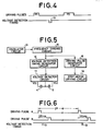
- FIG. 5 illustrates schematically an integrated circuit of an electronic timepiece according to the present invention.
- a reference timing signal produced by an oscillator circuit 14 is frequency divided by a frequency dividing circuit 15.
- An output signal of the frequency dividing circuit 15 is supplied to a voltage detection timing generator circuit 16 and a driving pulse generator circuit 18.
- a voltage detector circuit 17 detects voltages VC2 and VC1 by a timing outputted from the voltage detection timing generator circuit 16.
- the driving pulse generator circuit 18 delivers driving pulses to a step motor driving circuit 19.
- This circuit 19 detects rotation and non-rotation of a step motor, while driving the same, and requests the driving pulse generator circuit 18 for a compensating drive pulse P2 when non-rotation is detected.
- the relationship between the timing of an output signal of the voltage detection timing generator circuit 16 and the timing of output of the driving pulse generator circuit 18 is shown in Figure 1.
- the timing of a detection pulse 13 of the voltage detector circuit 17, which is the output of the voltage detection timing generating circuit 16 is set at 7.8 ms after the rise of the main drive pulse P1 while the timing for shifting between states (1) and (2) is set at 0.48 ms after the start of voltage detection.
- a time of 22.97 ms is left until the output of the compensating drive pulse P2 after the shift between states.
- Charge stored in the capacitor 2 in the above time period is 4.59 micro C when a charging current is 200 micro A.
- the charge of 4.59 micro C can raise the terminal voltage VC2 of the capacitor 2 by about 0.67V when the capacity of the capacitor 2 is 6.8 micro F, for instance. Accordingly, even when the terminal voltage
- the present invention is effected not only for a compensated drive system of electronic timepiece, but also for a construction in which cell life is displayed by an electronic timepiece.
- Figure 6 shows a driving waveform in the case where cell life of the electronic timepiece is displayed.
- the second drive of those given with a period of 2 seconds cannot be compensated if the detection of voltage is executed during a period of 1.825 second after a first drive pulse P to a following drive pulse A. Therefore, the detection of voltage is designed to be conducted during a period of 125 ms which forms a narrow interval of driving, as shown in Figure 6.
- the detection of voltage conducted within said short interval enables the compensation of drive conducted just after detection.
- the probability of stoppage of the electronic timepiece or failure of rhythmic movement of time indicating hands in the initial state of charging can be reduced, and thus the efficiency of the electronic timepiece with charging function can be improved.
Landscapes
- Physics & Mathematics (AREA)
- General Physics & Mathematics (AREA)
- Engineering & Computer Science (AREA)
- Power Engineering (AREA)
- Electromechanical Clocks (AREA)
- Direct Current Feeding And Distribution (AREA)
Abstract
Description
- This invention relates to analog electronic timepieces with charging function.
- One example of a charging circuit of an electronic timepiece with charging function employed heretofore is shown in Figure 2.
- In a first state of charging each of a plurality of switches a,b,c which may be MOSFETs are open. Accordingly, a
capacitor 2 having a relatively small capacitance is charged with electric energy generated by a solar cell 1. When the voltage VC₂ on thecapacitor 2 rises, an integratedcircuit 3 begins to operate. This will be referred to as state (1). When the voltage VC₂ on thecapacitor 2 exceeds a predetermined value after the integratedcircuit 3 begins to operate, the switch a is closed, and acapacity 4 of relatively large capacitance starts to charge. This will be referred to as stage (2). In the meantime the integratedcircuit 3 drives a step motor (not shown) to perform a time keeping operation. - In states (1) and (2) the integrated
circuit 3 and the step motor are driven by the charge accumulated on thecapacitor 2 and/or thecapacitor 4. - The capacitance of the
capacitor 2 used herein is set to be very small, about 6.8 micro F, for example, for the purpose of reducing the time for starting operation of the integratedcircuit 3. - It will be assumed that the shift from state (1) to state (2) occurs when the absolute value of the terminal voltage |VC₂| of the
capacitor 2 exceeds 2.0V. Further, it will be assumed that the solar cell 1 ceases to be irradiated with light for several seconds at the moment of rise of the terminal voltage |VC₂| above 2.0V brings about the shift to state (2) and thus electric energy ceases to be generated by the solar cell. The terminal voltage |VC₂| of thecapacitor 2 falls to approximately 0.9V after having driven the step motor several times. If no measures are taken in this condition the voltage VC₂ falls below the lowest operating voltage of the step motor, which causes operation to cease or failure of rhythmic movement of time indicating hands (not shown) driven by the step motor. - Even when the solar cell is again irradiated with light, the terminal voltage |VC₂| of the
capacitor 2 rises very slowly since thelarge capacitance capacitor 4 is connected in parallel across the solar cell 1. Consequently the operation of the step motor ceases for a relatively long time. The capacitance of thecapacitor 4 used herein is set to be about 0.3 F, for instance. Accordingly, it takes about 10 minutes for the current of 200 micro A to raise the voltage of thecapacitor 4 from, for example, 0.9V to 1.3V which enables operation of the step motor. During this period the electronic timepiece cannot be restarted. - In order to prevent this occurrence the voltage VC₂ is detected in state (2) and when VC₂ falls to a predetermined value or below, the switch a is opened to restore state (1). As a result, the
capacitor 2 receives all the electric energy generated by the solar cell 1 and therefore the terminal voltage of |VC₂| of thecapacitor 2 will be raised in a relatively short time. Accordingly, states (1) and (2) alternate in accordance with a balance between electric energy generated by the solar cell and electric energy consumed by the electronic timepiece in the initial state of charging. - The timing of detection of the voltage VC₂, the tiring in state (2) in particular, is at issue. Figure 3 shows the prior art voltage detecting timing. This shows the timing of a drive pulse in a compensated driving system in which a compensating drive pulse P₂ is outputted when the step motor is not rotated by a main driving pulse P₁. Such a compensated driving system is a requisite for an electronic timepiece with charging function in order to reduce power requirements.
- The prior art voltage detection timing is executed after the end of driving of the step motor, as shown by a
voltage detection pulse 12 in Figure 3 (the plurality of thepulse 12 means nothing in particular). Diodes 7,8 in Figure 2 are reverse-current check diodes which prevent an ineffective current bypassing the integratedcircuit 3. - The switch b and the switch care used in an advanced state of charging. These switches b and cwill not be described herein, because they have no direct relation with the description of the present invention.
- In the case where voltage detection is conducted after a compensating drive pulse P₂ is produced as shown in Figure 3, it sometimes happens that the compensating pulse P₂ cannot rotate the step motor. Assume, for instance, that the condition for a shift from state (2) to state (1) is |VC₂| ≦ 1.3V. If |VC₂| = 1.31V and the pulse width of the main drive pulse P₁ is 4 ms, |VC₂| is lowered to approximately 1.5V by the production of the main drive pulse P₁. If the lowest drive voltage for rotating the step motor is 1.2V, the step motor will not be rotated in this instance by the compensating drive pulse P₂.
- Since the condition |VC₂| ≦ 1.3V is detected by the
voltage detection pulse 12 and the shift is made from state (2) to state (1), thereafter, the potential VC₂ rises rapidly, so that there is sufficient energy to create the next drive pulse. However, the next drive pulse also fails to rotate the step motor due to failure of the preceding drive pulse, thus relating in a delay of 2 seconds. - According to the present invention there is provided an analog electronic timepiece with charging function comprising: an electric energy generating means; a plurality of capacitor means for storing electric energy generated by said electric energy generating means; and a voltage detector circuit means for detecting the voltages on said plurality of capacitor means, characterised by a driving pulse generator circuit means for generating a plurality of drive pulses for a step motor, wherein said drive pulses consist of relatively wide interval pulses and relatively narrow interval pulses; and a voltage detection timing generator circuit means for determining a detection timing of said voltage detector circuit means.
- Said voltage detector circuit means may be arranged to carry out voltage detection at said relatively narrow pulses.
- Said electric energy generating means may comprise a solar cell or a manually operated generator.
- Said plurality of capacitor means preferably comprises a first capacitor having a relatively large capacitance and arranged to be connected to and disconnected from said electric energy generating means according to the output of said voltage detector circuit means, and a second capacitor having a relatively small capacitance.
- The invention is illustrated, merely by way of example, in the accompanying drawings, in which:-
- Figure 1 shows the relationship between drive pulses and timing of voltage detection in an electronic timepiece according to the present invention;
- Figure 2 is a connection diagram of a conventional charging circuit of an electronic timepiece;
- Figure 3 shows the timing of voltage detection according to the conventional electronic timepiece;
- Figure 4 shows the timing of voltage detection of an electronic timepiece according to the present invention;
- Figure 5 is a block diagram showing schematically the function of an integrated circuit of an electronic timepiece according to the present invention; and
- Figure 6 shows driving waveforms and timing of voltage detection in the case where cell life display is conducted in an electronic timepiece according to the present invention.
- In order to solve the above described problem of an analog electronic timepiece with charging function employed heretofore, the present invention is designed to detect voltage between the main driving pulse P₁ and the compensating drive pulse P₂ so as to ensure that the compensating drive pulse P₂ rotates the step motor.
- The timing of the
voltage detection pulse 13 is set, as shown in Figure 4, between the main drive pulse P₁ and the compensating drive pulse P₂. As a result, state (1) is restored owing to voltage detection being executed before the compensating drive pulse P₂, although the potential |VC₂| reduces below the lowest operating voltage of the step motor, under the same condition as described above. - On the assumption that the time from voltage detection to the output of the compensating drive pulse P₂ is 10 ms, for example, and the generated current of 200 micro A flows, the terminal voltage |VC₂| can be restored from a 1.05 V to approximately 1.31V until the compensating drive pulse P₂ rises. Therefore the step motor is driven normally by the compensating drive pulse P₂.
- Figure 5 illustrates schematically an integrated circuit of an electronic timepiece according to the present invention. A reference timing signal produced by an oscillator circuit 14 is frequency divided by a
frequency dividing circuit 15. An output signal of thefrequency dividing circuit 15 is supplied to a voltage detectiontiming generator circuit 16 and a drivingpulse generator circuit 18. Avoltage detector circuit 17 detects voltages VC₂ and VC₁ by a timing outputted from the voltage detectiontiming generator circuit 16. - The driving
pulse generator circuit 18 delivers driving pulses to a stepmotor driving circuit 19. Thiscircuit 19 detects rotation and non-rotation of a step motor, while driving the same, and requests the drivingpulse generator circuit 18 for a compensating drive pulse P₂ when non-rotation is detected. - The relationship between the timing of an output signal of the voltage detection
timing generator circuit 16 and the timing of output of the drivingpulse generator circuit 18 is shown in Figure 1. For instance, the timing of adetection pulse 13 of thevoltage detector circuit 17, which is the output of the voltage detectiontiming generating circuit 16, is set at 7.8 ms after the rise of the main drive pulse P₁ while the timing for shifting between states (1) and (2) is set at 0.48 ms after the start of voltage detection. By these settings, a time of 22.97 ms is left until the output of the compensating drive pulse P₂ after the shift between states. - Charge stored in the
capacitor 2 in the above time period is 4.59 micro C when a charging current is 200 micro A. The charge of 4.59 micro C can raise the terminal voltage VC₂ of thecapacitor 2 by about 0.67V when the capacity of thecapacitor 2 is 6.8 micro F, for instance. Accordingly, even when the terminal voltage |VC₂| of thecapacitor 2 is lowered sharply by generation of the main drive pulse P₁, the voltage VC₂ can be raised by the time the following compensating drive pulse P₂ is generated when the solar cell is irradiated with light. - The present invention is effected not only for a compensated drive system of electronic timepiece, but also for a construction in which cell life is displayed by an electronic timepiece.
- Figure 6 shows a driving waveform in the case where cell life of the electronic timepiece is displayed. In this case also, it sometimes happens that the second drive of those given with a period of 2 seconds cannot be compensated if the detection of voltage is executed during a period of 1.825 second after a first drive pulse P to a following drive pulse A. Therefore, the detection of voltage is designed to be conducted during a period of 125 ms which forms a narrow interval of driving, as shown in Figure 6.
- As above described, it is necessary for improving the quality or efficiency of electronic timepieces, to set the timing of voltage detection in the period forming a narrow interval of driving in the case of an analog electronic timepiece with charging function based on the compensated driving system or conducting cell life display, which is driven at a relatively wide driving interval and at a relatively narrow driving interval.
- It is relatively very easy to determine the timing of voltage detection from the output timing of the driving
pulse generator circuit 18, by modifying the construction of a logic circuit of the voltage detection tiringgenerator circuit 16. - As above described, in the case where there is a possibility of a step motor being driven at a shorter interval than an ordinary period of operation of time indicating hands as in the compensated driving system, the detection of voltage conducted within said short interval enables the compensation of drive conducted just after detection. As a result, the probability of stoppage of the electronic timepiece or failure of rhythmic movement of time indicating hands in the initial state of charging can be reduced, and thus the efficiency of the electronic timepiece with charging function can be improved.
Claims (5)
Applications Claiming Priority (2)
| Application Number | Priority Date | Filing Date | Title |
|---|---|---|---|
| JP80723/86 | 1986-04-08 | ||
| JP61080723A JPS62237384A (en) | 1986-04-08 | 1986-04-08 | Analog electronic timepiece with charging function |
Publications (3)
| Publication Number | Publication Date |
|---|---|
| EP0241202A2 true EP0241202A2 (en) | 1987-10-14 |
| EP0241202A3 EP0241202A3 (en) | 1989-12-06 |
| EP0241202B1 EP0241202B1 (en) | 1993-06-02 |
Family
ID=13726282
Family Applications (1)
| Application Number | Title | Priority Date | Filing Date |
|---|---|---|---|
| EP87302774A Expired - Lifetime EP0241202B1 (en) | 1986-04-08 | 1987-03-31 | Analog electronic timepiece with charging function |
Country Status (4)
| Country | Link |
|---|---|
| US (1) | US4760564A (en) |
| EP (1) | EP0241202B1 (en) |
| JP (1) | JPS62237384A (en) |
| DE (1) | DE3786035T2 (en) |
Cited By (3)
| Publication number | Priority date | Publication date | Assignee | Title |
|---|---|---|---|---|
| EP0320754A1 (en) * | 1987-12-11 | 1989-06-21 | Asulab S.A. | Device for rewinding the main spring of a clockwork comprising a photo-electric cell |
| GB2211679A (en) * | 1987-10-27 | 1989-07-05 | Eric Paul Paterson | Solar powered current supply circuit |
| EP0420796B1 (en) * | 1989-09-26 | 1993-04-14 | LEMRICH & CIE S.A. | Electronic timepiece |
Families Citing this family (10)
| Publication number | Priority date | Publication date | Assignee | Title |
|---|---|---|---|---|
| JPH07130400A (en) * | 1993-11-02 | 1995-05-19 | Fuji Photo Film Co Ltd | Non-aqueous electrolyte battery charging method and charging device |
| DE69511649T2 (en) * | 1994-04-06 | 2000-04-06 | Citizen Watch Co., Ltd. | ELECTRONIC CLOCK |
| CH690523A5 (en) * | 1996-12-09 | 2000-09-29 | Asulab Sa | Timepiece including a generator of electricity. |
| JP4343549B2 (en) * | 2003-02-24 | 2009-10-14 | セイコーインスツル株式会社 | Step motor control device and electronic timepiece |
| JP4236956B2 (en) * | 2003-02-24 | 2009-03-11 | セイコーインスツル株式会社 | Step motor control device and electronic timepiece |
| JP4542370B2 (en) * | 2004-05-24 | 2010-09-15 | オリンパス株式会社 | Intra-subject introduction device |
| JP4800787B2 (en) * | 2006-02-15 | 2011-10-26 | セイコーインスツル株式会社 | Step motor drive circuit and analog electronic timepiece |
| US8111033B2 (en) * | 2008-06-17 | 2012-02-07 | Seiko Instruments Inc. | Stepping motor control circuit and analog electronic timepiece |
| JP2012078343A (en) * | 2010-09-08 | 2012-04-19 | Seiko Instruments Inc | Drive controller, clocking device, and electronic equipment |
| CN105607461B (en) * | 2014-11-13 | 2019-04-16 | 精工电子有限公司 | The control method of electronic watch and electronic watch |
Family Cites Families (8)
| Publication number | Priority date | Publication date | Assignee | Title |
|---|---|---|---|---|
| JPS53132386A (en) * | 1977-04-23 | 1978-11-18 | Seiko Instr & Electronics Ltd | Electronic watch |
| US4240021A (en) * | 1977-05-20 | 1980-12-16 | Citizen Watch Co., Ltd. | Solar cell battery charging control system |
| JPS5643575A (en) * | 1979-09-18 | 1981-04-22 | Seiko Instr & Electronics Ltd | Electronic clock |
| JPS5743526A (en) * | 1980-08-27 | 1982-03-11 | Seiko Instr & Electronics | Charge control circuit |
| CH642808B (en) * | 1981-01-05 | 1900-01-01 | Rolex Montres | PROCESS FOR DETERMINING THE DISCHARGE STATE OF AN ELECTRIC BATTERY AND DEVICE FOR IMPLEMENTING THIS PROCESS. |
| CH646576GA3 (en) * | 1981-10-02 | 1984-12-14 | ||
| US4634953A (en) * | 1984-04-27 | 1987-01-06 | Casio Computer Co., Ltd. | Electronic equipment with solar cell |
| NL8402113A (en) * | 1984-07-03 | 1986-02-03 | Kinetron Bv | SYSTEM FOR ELECTRICAL SUPPLY OF PORTABLE MINIATURE ENERGY CONSUMERS. |
-
1986
- 1986-04-08 JP JP61080723A patent/JPS62237384A/en active Granted
-
1987
- 1987-03-31 EP EP87302774A patent/EP0241202B1/en not_active Expired - Lifetime
- 1987-03-31 DE DE8787302774T patent/DE3786035T2/en not_active Expired - Fee Related
- 1987-04-06 US US07/035,088 patent/US4760564A/en not_active Expired - Lifetime
Cited By (4)
| Publication number | Priority date | Publication date | Assignee | Title |
|---|---|---|---|---|
| GB2211679A (en) * | 1987-10-27 | 1989-07-05 | Eric Paul Paterson | Solar powered current supply circuit |
| EP0320754A1 (en) * | 1987-12-11 | 1989-06-21 | Asulab S.A. | Device for rewinding the main spring of a clockwork comprising a photo-electric cell |
| CH671496GA3 (en) * | 1987-12-11 | 1989-09-15 | ||
| EP0420796B1 (en) * | 1989-09-26 | 1993-04-14 | LEMRICH & CIE S.A. | Electronic timepiece |
Also Published As
| Publication number | Publication date |
|---|---|
| JPH045956B2 (en) | 1992-02-04 |
| DE3786035D1 (en) | 1993-07-08 |
| DE3786035T2 (en) | 1993-09-09 |
| EP0241202A3 (en) | 1989-12-06 |
| US4760564A (en) | 1988-07-26 |
| JPS62237384A (en) | 1987-10-17 |
| EP0241202B1 (en) | 1993-06-02 |
Similar Documents
| Publication | Publication Date | Title |
|---|---|---|
| EP0194136B1 (en) | Electronic timepiece with a solar cell | |
| US5889734A (en) | Electronic timepiece | |
| EP0326313B1 (en) | Wrist watch | |
| EP0241202B1 (en) | Analog electronic timepiece with charging function | |
| US4785435A (en) | Self-chargeable electronic timepiece with operating voltage checking | |
| JP3623397B2 (en) | Electronic watch and its charging method | |
| GB2149942A (en) | Electronic timepiece | |
| CN1319242C (en) | Electronic device, electronic timepiece and power control method | |
| EP1542099B1 (en) | Electronic clock | |
| GB2158274A (en) | Electronic timepiece | |
| JP2940546B2 (en) | Electronic clock with generator | |
| JP3592371B2 (en) | Solar clock | |
| GB2159351A (en) | Charge/discharge circuit | |
| JPS62242882A (en) | Electronic timepiece | |
| JP2534484B2 (en) | Electronic watch with charging device | |
| JP3673318B2 (en) | Rechargeable watch and power supply method | |
| JPH05264751A (en) | Analog electronic clock | |
| JP3592359B2 (en) | Solar clock | |
| JP3706622B2 (en) | Solar clock | |
| JP4564122B2 (en) | Electronic clock | |
| JPH03148092A (en) | electronic clock | |
| JPH0797141B2 (en) | How to display the charge status of an electronic watch | |
| JP3017541B2 (en) | Electronic clock | |
| JP2004135497A (en) | Electronic device, electronically controlled timepiece, and power supply control method | |
| JPH0631725B2 (en) | Electronic clock with charging function |
Legal Events
| Date | Code | Title | Description |
|---|---|---|---|
| PUAI | Public reference made under article 153(3) epc to a published international application that has entered the european phase |
Free format text: ORIGINAL CODE: 0009012 |
|
| AK | Designated contracting states |
Kind code of ref document: A2 Designated state(s): CH DE GB LI |
|
| PUAL | Search report despatched |
Free format text: ORIGINAL CODE: 0009013 |
|
| AK | Designated contracting states |
Kind code of ref document: A3 Designated state(s): CH DE GB LI |
|
| 17P | Request for examination filed |
Effective date: 19900525 |
|
| 17Q | First examination report despatched |
Effective date: 19910711 |
|
| GRAA | (expected) grant |
Free format text: ORIGINAL CODE: 0009210 |
|
| AK | Designated contracting states |
Kind code of ref document: B1 Designated state(s): CH DE GB LI |
|
| REF | Corresponds to: |
Ref document number: 3786035 Country of ref document: DE Date of ref document: 19930708 |
|
| PLBE | No opposition filed within time limit |
Free format text: ORIGINAL CODE: 0009261 |
|
| STAA | Information on the status of an ep patent application or granted ep patent |
Free format text: STATUS: NO OPPOSITION FILED WITHIN TIME LIMIT |
|
| 26N | No opposition filed | ||
| REG | Reference to a national code |
Ref country code: GB Ref legal event code: IF02 |
|
| PGFP | Annual fee paid to national office [announced via postgrant information from national office to epo] |
Ref country code: GB Payment date: 20030326 Year of fee payment: 17 |
|
| PGFP | Annual fee paid to national office [announced via postgrant information from national office to epo] |
Ref country code: CH Payment date: 20030331 Year of fee payment: 17 |
|
| PGFP | Annual fee paid to national office [announced via postgrant information from national office to epo] |
Ref country code: DE Payment date: 20030409 Year of fee payment: 17 |
|
| PG25 | Lapsed in a contracting state [announced via postgrant information from national office to epo] |
Ref country code: LI Free format text: LAPSE BECAUSE OF NON-PAYMENT OF DUE FEES Effective date: 20040331 Ref country code: GB Free format text: LAPSE BECAUSE OF NON-PAYMENT OF DUE FEES Effective date: 20040331 Ref country code: CH Free format text: LAPSE BECAUSE OF NON-PAYMENT OF DUE FEES Effective date: 20040331 |
|
| PG25 | Lapsed in a contracting state [announced via postgrant information from national office to epo] |
Ref country code: DE Free format text: LAPSE BECAUSE OF NON-PAYMENT OF DUE FEES Effective date: 20041001 |
|
| REG | Reference to a national code |
Ref country code: CH Ref legal event code: PL |
|
| GBPC | Gb: european patent ceased through non-payment of renewal fee |