EP0238247B1 - Method for measuring dimensions of fine pattern - Google Patents
Method for measuring dimensions of fine pattern Download PDFInfo
- Publication number
- EP0238247B1 EP0238247B1 EP87302042A EP87302042A EP0238247B1 EP 0238247 B1 EP0238247 B1 EP 0238247B1 EP 87302042 A EP87302042 A EP 87302042A EP 87302042 A EP87302042 A EP 87302042A EP 0238247 B1 EP0238247 B1 EP 0238247B1
- Authority
- EP
- European Patent Office
- Prior art keywords
- pattern
- pattern image
- image
- displayed
- line
- Prior art date
- Legal status (The legal status is an assumption and is not a legal conclusion. Google has not performed a legal analysis and makes no representation as to the accuracy of the status listed.)
- Expired
Links
Images


Classifications
-
- G—PHYSICS
- G01—MEASURING; TESTING
- G01B—MEASURING LENGTH, THICKNESS OR SIMILAR LINEAR DIMENSIONS; MEASURING ANGLES; MEASURING AREAS; MEASURING IRREGULARITIES OF SURFACES OR CONTOURS
- G01B11/00—Measuring arrangements characterised by the use of optical techniques
- G01B11/02—Measuring arrangements characterised by the use of optical techniques for measuring length, width or thickness
- G01B11/024—Measuring arrangements characterised by the use of optical techniques for measuring length, width or thickness by means of diode-array scanning
Definitions
- the present invention relates to a method for measuring dimensions of a fine pattern of, for example, integrated circuits (IC's) or semiconductors, etc. More precisely, the present invention relates to a method for measuring the dimensions of a fine pattern or patterns displayed on a display unit, such as a monitor TV by an optical image forming system.
- IC's integrated circuits
- semiconductors etc. More precisely, the present invention relates to a method for measuring the dimensions of a fine pattern or patterns displayed on a display unit, such as a monitor TV by an optical image forming system.
- the fine patterns such as contact holes, are usually reproduced on an enlarged scale on a screen of a monitor TV by an optical image forming system. Namely, enlarged dimensions of the fine patterns are optically displayed on the TV screen.
- the fine patterns are usually designed to be rectangular- or square-shaped, as is well known.
- circular patterns are formed on the wafer, etc., in place of the intended angular patterns, mainly because of a limited resolving power of the optical system used, or a limited etching precision or development, during the wafer manufacturing process. Namely, it is impossible or next to impossible to exactly reproduce an angular fine pattern as designed.
- the deviation or deformation of the pattern images on the monitor screen which is mainly caused by a failure or inaccuracy of the positioning or adjustment of the optical image forming system, as mentioned above, results in incorrect dimensional measurement of the patterns.
- An embodiment of the present invention may, therefore, provide a precise and reliable measuring method which is free from the aforementioned drawbacks of the prior art.
- a method for controlling a fine pattern comprising detecting the surface area and the profile of a displayed pattern image, determining the center of gravity of the displayed pattern image, determining the equivalent diameter of a circular pattern having the same surface area as the displayed patern image, determining the mean value of pattern lengths of lines which pass through the center of gravity of the displayed pattern image and which intersect the displayed profiler of the pattern image at two points of intersection, and comparing the obtained mean value with the equivalent diameter of the displayed pattern image.
- the pattern lengths are conveniently defined as distances between the two points of intersection.
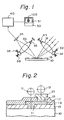
- Figure 2 shows an IC wafer 10 having contact holes II and 13, to be measured.
- the wafer 10 has an insulation layer 15 thereon, and having a contact hole or contact holes II in which an electrode 17 is formed.
- On the insulation layer 15 and the electrode 17 is formed another insulation layer 19 having a contact hole or contact holes 13 in which an electrode 21 is formed, to establish an electrical connection between the .two electrodes 17 and 21 through the contact holes II and 13.
- the contact holes II and 13 are fine circular patterns, as mentioned above.
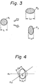
- the displayed pattern 100 is not a true circle but is slightly deformed, i.e., an elliptical pattern, as mentioned before.
- Figure I shows an optical image forming system in which a light beam from a light source (not shown) is focused on the wafer 10 having the insulation layer 15 having the contact hole II to be measured, by means of a focusing lens 31.
- a light beam from a light source (not shown) is focused on the wafer 10 having the insulation layer 15 having the contact hole II to be measured, by means of a focusing lens 31.
- measuring is effected before the insulation layer 19 is formed on the insulation layer 15 and on the electrode 17.
- the light beams reflected by the wafer 10 and the insulation layer 15 are displayed on a charge-coupled device image sensor (CCD) image sensor) 35 by an imaging lens 33.
- CCD-image sensor 35 produces electrical charges when a light beam is focused thereon, to create image signals.
- the output signal of the CCD image sensor 35 is fed to a control unit 40 which feeds the image signals to the monitor TV 50, so that a pattern image 100 is displayed on the screen 51 of the TV 50 in accordance with the fine pattern formed on the wafer 10. Then, the pattern 100 displayed on the monitor screen 51 is measured by a measuring method embodying the present invention.
- the circular pattern PI formed on the wafer 10 is displayed as an elliptical image patterns P2 and P3 on the monitor screen, as shown in Fig. 3. Consequently, the actually measured dimensions (diameters) LI and L2 are different from the real diameter L of the circular pattern Pl. Accordingly, it can not be determined whether the dimensions of the fine pattern PI formed on the wafer 10 are identical to a design value.
- the inventors of the present invention have discovered that, when pattern dimensions which are calculated from the surface area of the pattern displayed on the monitor screen are substantially identical to mathematical mean values of pattern dimensions which are measured along lines passing through the center of gravity of the pattern, the pattern image displayed on the monitor screen substantially correctly represents the actual pattern formed on the wafer.
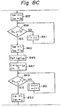
- FIG. 7 shows a flow chart of the process carried out in the control unit 40 (Fig. I), in a method embodying the invention.
- step 701 the image data from the CCD image sensor 35 are fetched into the control unit (computer) 40, and then at step 703, a surface area A of the pattern image is displayed on the monitor screen 51, and is detected by the CCD image sensor 35 at step 705.
- the CCD image sensor 35 has a large number of photoelectric devices 35a (Fig. 5) which are in a matrix arrangement and which are given predetermined addresses (i, j) in an X-Y coordinate.
- the surface area of the pattern image displayed on the monitor screen can be obtained by counting the number of photoelectric devices (picture elements) 35a activated when the light beam impinges thereon.
- the picture elements 35a are designed so that when, for example, the light beam impinges on more than half the surface area of each picture element 35a, that element 35a issues image signals (image data).
- the accuracy of the detection of the surface area of the pattern image displayed on the monitor screen can be easily increased by increasing the density of the matrix arrangement of the picture elements 35a.
- the outline (profile) of the pattern image displayed on the monitor screen can be also determined by the picture elements 35a, which are activated when the light beam impinges on more than half the surface area thereof.
- the center of gravity G(i G , j G ) of the pattern image is detected.
- the center of gravity G can be easily mathematically obtained by the following equations: wherein ai,j are image data which is "I" when the picture elements 35a are activated, i.e., when the light beam impinges on more than half the surface area of the picture elements 35a, and which is "0" when the picture elements 35a are not activated, i.e.
- n the number of picture elements 35a along the X-axis (ordinate) and the Y-axis (abscissa) in the coordinate (Fig. 5).
- the number of picture elements 35a is identical in the ordinate and in the abscissa.
- a difference in the number of the picture elements 35a between in the ordinate and in the abscissa can be made.
- the origin O of the coordinate is represented by (0,0) in Fig. 5.
- an equivalent diameter D A of the generally elliptical pattern image PI or P2 displayed on the screen is calculated.
- the equivalent diameter D A is a diameter of an equivalent circle having the same surface area A as the pattern image measured at step 705.
- the equivalent diameter D A can be easily obtained from the following equation: wherein, A is a surface area of the pattern image measured at step 705.
- step 711 actual lengths D 1 , D 2 , ... D n of lines x 1 , x 2 , ... x n (Fig. 4) which pass the center of gravity G and extend between two extremities at which the lines intersect the profile of the pattern image, are measured.
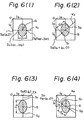
- step 711 for the detection of the pattern length Details of step 711 for the detection of the pattern length are shown in Fig. 8.
- Fig. 8 the detection of only four pattern lengths Di , D 2 , Da , and D 4 of four lines xi , x 2 , x 3 and X 4 , which are spaced at an equiangular distance of 45 ° , is shown for clarification.
- the line X 1 is successively shifted by 45° in the counterclockwise direction to assume the positions x 2 , X 3 , and x 4 , respectively.
- step 801 the line x i is determined.
- the line x i intersects the X-axis at a point So , which is represented by (i G , 0).
- step 803 if a i,j is "0" the control proceeds to step 805, which counts the abscissa up by I and returns the flow to step 803.
- the data ai,j becomes "I” only when the line extends within the profile of the pattern image.
- step 815 the line x 2 is determined, which is angularly spaced from the line X 1 by 45 ° .
- the line x 2 intersects the X-axis at a point So which is represented by (i G + j G , 0), since the ordinate of the point So is (iG + jG).
- step 819 the control proceeds to step 819 which counts both the ordinate and the abscissa down and up by I, respectively and returns the flow to step 815.
- step 815 if ai,j is "I”, the control proceeds to step 821, which causes values (isi , jsl) of a first intersecting point S i in which the line x 2 first intersects the profile of the pattern image to be i and j, respectively.
- step 823 if the data ai,j is "I”, the control proceeds to step 825, which counts the ordinate and the abscissa down and up by I, respectively. If ai,j is "0" at step 823, values (i S2 , j S2 ) of a second intersecting point S 2 , at which the line X 2 again intersects the profile of the pattern image, are caused to be i and j, respectively at the step 827. Thus, the pattern length D 2 of the line x 2 is obtained form the distance between the points PI and P2, i.e. from at step 829.
- the third line xs is determined, which is angularly spaced from the second line x 2 by 45°.
- the line X 3 intersects the Y-axis (abscissa) at the point So , which is represented by (0, j G ). If ai,j is "0" at step 833, the control proceeds to step 835 which counts the ordinate up by I and returns the flow to step 833. At step 833, if ai,j is "I”, the control proceeds to step 837, which causes values (isl , jsl) of a first intersecting point S 1 in which the line X 3 first intersents the profile of the pattern image to be i and j G , respectively.
- the fourth line X 4 is determined which is angularly spaced from the third line x 3 by 45°.
- the line X 4 intersects the X-axis (ordinate) at the starting point So , which is represented by (i G - jG , 0), subsequently, if ai,j is "0" at step 849, the control proceeds to step 851 which counts the ordinate and the abscissa up by I and returns the flow to step 849.
- step 849 if ai,j is "I”, the control proceeds to step 853, which causes values (isl , jsl) of a first intersecting point S 1 in which the line X 4 first intersects the profile of the pattern image to be i and j, respectively.
- step 855 if the data ai,j is "I", the control proceeds to step 857, which counts th ordinate and the abscissa up by I. If ajj is "0" at step 855, values (is 2 , js 2 ) of a second intersecting points S 2 , at which the line X4 again intersects the profile of the pattern image, are caused to be i and j, respectively at step 859. the data aii becomes "0" when the line X4 intersects the profile of the pattern image at the second intersecting point S 2 .
- the pattern length D 4 of the line X4 obtained from the distance between the points PI and P2, i.e., from D 4 at step 861.
- the detection of the pattern length at step 711 is completed at step 863.
- a mean value D a of the pattern lengths D 1 , D 2 , D 3 , ... D n is detected.
- the mean value can be obtained from the following equation:
- step 715 the mean value D a thus obtained is compared with the equivalent diameter D A obtained at step 709. If a difference between D a and D A is below a predetermined limit value T at step 717, the control proceeds to step 719 which outputs a display "good", which means that the pattern image on the wafer is correctly displayed on the monitor screen by the optical image forming system.
- the adjustment of the optical system includes, for example, an adjustment of the optical axis of the light source, an adjustment of lens angles of the lenses 31 and 33 with respect to the light beams incident thereupon, or an adjustment of lens centers of the lenses 31 and 33.
- the lenses 31 and 33 are supported at one ends by springs 43 and 45 for universal movement.
- the opposite ends of the lenses 31 and 33 are provided with adjusting screws 32, 34 and 36, 38.
- the adjusting screws 32 and 36 adjust the lens angles of the lenses 31 and 33 with respect to the light beams incident thereupon.
- the adjusting screws 34 and 38 adjust the lens centers of the lenses 31 and 33 in the lens axis directions.
- the lenses 31 and 33 can be provided with additional adjusting screws (not shown) which adjust the lens position in the direction perpendicular to the directions of adjustment by the adjusting screws 32, 34 and 36, 38, respectively.
- the operator can manually adjust the adjusting screws in accordance with the display at steps 719 and 721.
- either the equivalent diameter D A or the mean value Da can be sued as an actual diameter of the substantially circular pattern formed on the wafer.
- the optical system reproduces the pattern on the display unit, such as monitor TV, with an increased precision.
- the present invention is not limited to the embodiments described above and illustrated in the drawings and can be applied to measure dimensions of any fine pattern, for example, that of a mask which forms the contact holes or through holes on the wafer mentioned above.
Landscapes
- Physics & Mathematics (AREA)
- General Physics & Mathematics (AREA)
- Length Measuring Devices By Optical Means (AREA)
Applications Claiming Priority (2)
| Application Number | Priority Date | Filing Date | Title |
|---|---|---|---|
| JP61051959A JPS62209304A (ja) | 1986-03-10 | 1986-03-10 | 寸法測定方法 |
| JP51959/86 | 1986-03-10 |
Publications (2)
| Publication Number | Publication Date |
|---|---|
| EP0238247A1 EP0238247A1 (en) | 1987-09-23 |
| EP0238247B1 true EP0238247B1 (en) | 1990-01-24 |
Family
ID=12901400
Family Applications (1)
| Application Number | Title | Priority Date | Filing Date |
|---|---|---|---|
| EP87302042A Expired EP0238247B1 (en) | 1986-03-10 | 1987-03-10 | Method for measuring dimensions of fine pattern |
Country Status (4)
| Country | Link |
|---|---|
| US (1) | US4790023A (enExample) |
| EP (1) | EP0238247B1 (enExample) |
| JP (1) | JPS62209304A (enExample) |
| DE (1) | DE3761515D1 (enExample) |
Families Citing this family (23)
| Publication number | Priority date | Publication date | Assignee | Title |
|---|---|---|---|---|
| GB8800570D0 (en) * | 1988-01-12 | 1988-02-10 | Leicester Polytechnic | Measuring method |
| US5340992A (en) * | 1988-02-16 | 1994-08-23 | Canon Kabushiki Kaisha | Apparatus and method of detecting positional relationship using a weighted coefficient |
| US4969200A (en) * | 1988-03-25 | 1990-11-06 | Texas Instruments Incorporated | Target autoalignment for pattern inspector or writer |
| IT1220409B (it) * | 1988-06-29 | 1990-06-15 | Gd Spa | Metodo per il controllo di estremita' di sigarette disposte ammassate |
| DE3835981A1 (de) * | 1988-10-21 | 1990-04-26 | Mtu Muenchen Gmbh | Verfahren zur pruefung der toleranzen von bohrungen |
| US5850465A (en) * | 1989-06-26 | 1998-12-15 | Fuji Photo Film Co., Ltd. | Abnormnal pattern detecting or judging apparatus, circular pattern judging apparatus, and image finding apparatus |
| US5231678A (en) * | 1989-11-15 | 1993-07-27 | Ezel, Inc. | Configuration recognition system calculating a three-dimensional distance to an object by detecting cross points projected on the object |
| US5164994A (en) * | 1989-12-21 | 1992-11-17 | Hughes Aircraft Company | Solder joint locator |
| US5231675A (en) * | 1990-08-31 | 1993-07-27 | The Boeing Company | Sheet metal inspection system and apparatus |
| US5288938A (en) * | 1990-12-05 | 1994-02-22 | Yamaha Corporation | Method and apparatus for controlling electronic tone generation in accordance with a detected type of performance gesture |
| JPH0750508A (ja) * | 1993-08-06 | 1995-02-21 | Fujitsu Ltd | アンテナモジュール |
| US6084986A (en) * | 1995-02-13 | 2000-07-04 | Eastman Kodak Company | System and method for finding the center of approximately circular patterns in images |
| US6072897A (en) * | 1997-09-18 | 2000-06-06 | Applied Materials, Inc. | Dimension error detection in object |
| US7262864B1 (en) * | 2001-07-02 | 2007-08-28 | Advanced Micro Devices, Inc. | Method and apparatus for determining grid dimensions using scatterometry |
| US7424902B2 (en) * | 2004-11-24 | 2008-09-16 | The Boeing Company | In-process vision detection of flaw and FOD characteristics |
| US20060108048A1 (en) * | 2004-11-24 | 2006-05-25 | The Boeing Company | In-process vision detection of flaws and fod by back field illumination |
| US8668793B2 (en) * | 2005-08-11 | 2014-03-11 | The Boeing Company | Systems and methods for in-process vision inspection for automated machines |
| US9052294B2 (en) * | 2006-05-31 | 2015-06-09 | The Boeing Company | Method and system for two-dimensional and three-dimensional inspection of a workpiece |
| US20070277919A1 (en) * | 2006-05-16 | 2007-12-06 | The Boeing Company | Systems and methods for monitoring automated composite manufacturing processes |
| US8050486B2 (en) * | 2006-05-16 | 2011-11-01 | The Boeing Company | System and method for identifying a feature of a workpiece |
| US8331648B2 (en) * | 2008-10-03 | 2012-12-11 | Patent Store Llc | Making sealant containing twist-on wire connectors |
| CN101979751B (zh) * | 2010-09-28 | 2012-07-25 | 中华人民共和国陕西出入境检验检疫局 | 基于图像分析的织物尺寸稳定性检测方法 |
| US11410281B1 (en) * | 2021-11-29 | 2022-08-09 | Unity Technologies Sf | Increasing dynamic range of a virtual production display |
Family Cites Families (9)
| Publication number | Priority date | Publication date | Assignee | Title |
|---|---|---|---|---|
| US3679820A (en) * | 1970-01-19 | 1972-07-25 | Western Electric Co | Measuring system |
| US4017721A (en) * | 1974-05-16 | 1977-04-12 | The Bendix Corporation | Method and apparatus for determining the position of a body |
| DE2542904A1 (de) * | 1975-09-26 | 1977-03-31 | Automationsanlagen Dipl Ing Kl | Verfahren zum pruefen eines gegenstandes |
| GB2067326B (en) * | 1980-01-09 | 1983-03-09 | British United Shoe Machinery | Workpiece identification apparatus |
| DE3587220T2 (de) * | 1984-01-13 | 1993-07-08 | Komatsu Mfg Co Ltd | Identifizierungsverfahren von konturlinien. |
| IT1179997B (it) * | 1984-02-24 | 1987-09-23 | Consiglio Nazionale Ricerche | Procedimento ed apparecchiatura per il rilievo dell impronta lasciata in un provino nella misura della durezza alla penetrazione |
| US4596037A (en) * | 1984-03-09 | 1986-06-17 | International Business Machines Corporation | Video measuring system for defining location orthogonally |
| JPS61293657A (ja) * | 1985-06-21 | 1986-12-24 | Matsushita Electric Works Ltd | 半田付け外観検査方法 |
| US4658428A (en) * | 1985-07-17 | 1987-04-14 | Honeywell Inc. | Image recognition template generation |
-
1986
- 1986-03-10 JP JP61051959A patent/JPS62209304A/ja active Granted
-
1987
- 1987-03-09 US US07/023,493 patent/US4790023A/en not_active Expired - Lifetime
- 1987-03-10 EP EP87302042A patent/EP0238247B1/en not_active Expired
- 1987-03-10 DE DE8787302042T patent/DE3761515D1/de not_active Expired - Lifetime
Also Published As
| Publication number | Publication date |
|---|---|
| DE3761515D1 (de) | 1990-03-01 |
| US4790023A (en) | 1988-12-06 |
| EP0238247A1 (en) | 1987-09-23 |
| JPS62209304A (ja) | 1987-09-14 |
| JPH044524B2 (enExample) | 1992-01-28 |
Similar Documents
| Publication | Publication Date | Title |
|---|---|---|
| EP0238247B1 (en) | Method for measuring dimensions of fine pattern | |
| EP0895279A1 (en) | Manufacture of semiconductor device | |
| EP0457843B1 (en) | Method and apparatus for measuring registration between layers of a semiconductor wafer | |
| US7180189B2 (en) | Abberation mark and method for estimating overlay error and optical abberations | |
| JP3181050B2 (ja) | 投影露光方法およびその装置 | |
| US7244623B2 (en) | Method of manufacturing semiconductor device and apparatus of automatically adjusting semiconductor pattern | |
| JP2009156877A (ja) | 三次元検査システム | |
| JPH0244137B2 (enExample) | ||
| CN112634373A (zh) | 基于零膨胀陶瓷标定板的视觉测量系统动态校正方法 | |
| US5978094A (en) | Alignment device and method based on imaging characteristics of the image pickup system | |
| CN115289997A (zh) | 一种双目相机三维轮廓扫描仪及其使用方法 | |
| US4845530A (en) | Reduced projection type step- and repeat-exposure apparatus | |
| JPS62110248A (ja) | 回転角度補正方法およびその装置 | |
| JP3258178B2 (ja) | 位置合わせ方法 | |
| US5929529A (en) | Reticle semiconductor wafer, and semiconductor chip | |
| JP2806242B2 (ja) | 電子線露光の位置合わせマークおよび電子線露光の位置合わせマークの検出方法 | |
| US6335785B1 (en) | Scan-type reducing projection exposure method and apparatus | |
| JPH11132735A (ja) | Icリード浮き検査装置及び検査方法 | |
| JP2549847B2 (ja) | 半導体装置の製造方法とこれに使用するパタ−ンパタ−ン寸法測定装置 | |
| JPH0145735B2 (enExample) | ||
| JP3084711B2 (ja) | 焦点検出装置 | |
| KR0136427B1 (ko) | 평면 스텝 모터를 이용한 노광 장비 스테이지의 미소 각도 보정장치 및 그 방법 | |
| KR19990084736A (ko) | 웨이퍼의 노광 포커스 정렬 방법 | |
| JP2513281B2 (ja) | 位置合わせ装置 | |
| JP2659704B2 (ja) | 露光装置 |
Legal Events
| Date | Code | Title | Description |
|---|---|---|---|
| PUAI | Public reference made under article 153(3) epc to a published international application that has entered the european phase |
Free format text: ORIGINAL CODE: 0009012 |
|
| AK | Designated contracting states |
Kind code of ref document: A1 Designated state(s): DE FR GB |
|
| 17P | Request for examination filed |
Effective date: 19880126 |
|
| 17Q | First examination report despatched |
Effective date: 19890512 |
|
| GRAA | (expected) grant |
Free format text: ORIGINAL CODE: 0009210 |
|
| AK | Designated contracting states |
Kind code of ref document: B1 Designated state(s): DE FR GB |
|
| ET | Fr: translation filed | ||
| REF | Corresponds to: |
Ref document number: 3761515 Country of ref document: DE Date of ref document: 19900301 |
|
| PLBE | No opposition filed within time limit |
Free format text: ORIGINAL CODE: 0009261 |
|
| STAA | Information on the status of an ep patent application or granted ep patent |
Free format text: STATUS: NO OPPOSITION FILED WITHIN TIME LIMIT |
|
| 26N | No opposition filed | ||
| PGFP | Annual fee paid to national office [announced via postgrant information from national office to epo] |
Ref country code: DE Payment date: 19940310 Year of fee payment: 8 |
|
| PG25 | Lapsed in a contracting state [announced via postgrant information from national office to epo] |
Ref country code: DE Effective date: 19951201 |
|
| REG | Reference to a national code |
Ref country code: GB Ref legal event code: IF02 |
|
| PGFP | Annual fee paid to national office [announced via postgrant information from national office to epo] |
Ref country code: GB Payment date: 20030305 Year of fee payment: 17 |
|
| PGFP | Annual fee paid to national office [announced via postgrant information from national office to epo] |
Ref country code: FR Payment date: 20030310 Year of fee payment: 17 |
|
| PG25 | Lapsed in a contracting state [announced via postgrant information from national office to epo] |
Ref country code: GB Free format text: LAPSE BECAUSE OF NON-PAYMENT OF DUE FEES Effective date: 20040310 |
|
| GBPC | Gb: european patent ceased through non-payment of renewal fee |
Effective date: 20040310 |
|
| PG25 | Lapsed in a contracting state [announced via postgrant information from national office to epo] |
Ref country code: FR Free format text: LAPSE BECAUSE OF NON-PAYMENT OF DUE FEES Effective date: 20041130 |
|
| REG | Reference to a national code |
Ref country code: FR Ref legal event code: ST |