EP0237694B1 - Agencement de circuit pour l'évaluation de signaux de courant alternatif obtenus à partir d'une source de signal - Google Patents
Agencement de circuit pour l'évaluation de signaux de courant alternatif obtenus à partir d'une source de signal Download PDFInfo
- Publication number
- EP0237694B1 EP0237694B1 EP19860890036 EP86890036A EP0237694B1 EP 0237694 B1 EP0237694 B1 EP 0237694B1 EP 19860890036 EP19860890036 EP 19860890036 EP 86890036 A EP86890036 A EP 86890036A EP 0237694 B1 EP0237694 B1 EP 0237694B1
- Authority
- EP
- European Patent Office
- Prior art keywords
- amplifiers
- signal source
- circuit
- amplifier
- voltage
- Prior art date
- Legal status (The legal status is an assumption and is not a legal conclusion. Google has not performed a legal analysis and makes no representation as to the accuracy of the status listed.)
- Expired
Links
- 238000011156 evaluation Methods 0.000 claims description 3
- 230000000694 effects Effects 0.000 description 3
- 238000004804 winding Methods 0.000 description 2
- 230000001629 suppression Effects 0.000 description 1
Images

Classifications
-
- H—ELECTRICITY
- H03—ELECTRONIC CIRCUITRY
- H03F—AMPLIFIERS
- H03F1/00—Details of amplifiers with only discharge tubes, only semiconductor devices or only unspecified devices as amplifying elements
- H03F1/52—Circuit arrangements for protecting such amplifiers
-
- G—PHYSICS
- G01—MEASURING; TESTING
- G01R—MEASURING ELECTRIC VARIABLES; MEASURING MAGNETIC VARIABLES
- G01R19/00—Arrangements for measuring currents or voltages or for indicating presence or sign thereof
- G01R19/0092—Arrangements for measuring currents or voltages or for indicating presence or sign thereof measuring current only
-
- H—ELECTRICITY
- H02—GENERATION; CONVERSION OR DISTRIBUTION OF ELECTRIC POWER
- H02H—EMERGENCY PROTECTIVE CIRCUIT ARRANGEMENTS
- H02H3/00—Emergency protective circuit arrangements for automatic disconnection directly responsive to an undesired change from normal electric working condition with or without subsequent reconnection ; integrated protection
- H02H3/26—Emergency protective circuit arrangements for automatic disconnection directly responsive to an undesired change from normal electric working condition with or without subsequent reconnection ; integrated protection responsive to difference between voltages or between currents; responsive to phase angle between voltages or between currents
- H02H3/32—Emergency protective circuit arrangements for automatic disconnection directly responsive to an undesired change from normal electric working condition with or without subsequent reconnection ; integrated protection responsive to difference between voltages or between currents; responsive to phase angle between voltages or between currents involving comparison of the voltage or current values at corresponding points in different conductors of a single system, e.g. of currents in go and return conductors
- H02H3/33—Emergency protective circuit arrangements for automatic disconnection directly responsive to an undesired change from normal electric working condition with or without subsequent reconnection ; integrated protection responsive to difference between voltages or between currents; responsive to phase angle between voltages or between currents involving comparison of the voltage or current values at corresponding points in different conductors of a single system, e.g. of currents in go and return conductors using summation current transformers
-
- H—ELECTRICITY
- H03—ELECTRONIC CIRCUITRY
- H03F—AMPLIFIERS
- H03F3/00—Amplifiers with only discharge tubes or only semiconductor devices as amplifying elements
- H03F3/68—Combinations of amplifiers, e.g. multi-channel amplifiers for stereophonics
Definitions
- the invention relates to a switching arrangement for evaluating AC signals obtained from a signal source, in which the signal source is connected to an amplifier arrangement having two amplifiers, the outputs of which are connected to one another and on the output side to a signal evaluation circuit, e.g. a threshold circuit is connected.
- a signal evaluation circuit e.g. a threshold circuit
- the object of the present invention is therefore to improve the behavior of a circuit arrangement for evaluating AC signals obtained from a signal source with respect to the quantities mentioned above.
- the signal source is connected to one of its two poles, each with an amplifier, the signal source being connected to the inputs of the amplifiers or, in the case of differential amplifiers, to their similar inputs and the remaining inputs of the differential amplifiers to one Reference potential are set, wherein each amplifier has a feedback formed by a parallel connection of a resistor with a diode and both diodes have the same forward direction.
- the differential amplifiers Due to the symmetrical use of the differential amplifiers, interference is practically compensated for itself, so that it can be found with amplifiers that are constructed much more simply. Furthermore, the parallel connection of a resistor with a diode in the feedback branch of a differential amplifier ensures that only positive voltages can occur at the output of the amplifier at its output, so that both amplifiers remain in the linear range.
- the amplifier inputs can be designed with very low impedance by appropriate dimensions of the feedback circuit.
- a preferred embodiment of the invention is that both amplifiers are supplied with the same supply voltage, the supply voltage being supplied to the two amplifiers via a PTC resistor, to which an ohmic resistor is also connected in series, and a voltage limiter circuit, e.g. a Zener diode, connected in parallel to the voltage source.
- a voltage limiter circuit e.g. a Zener diode
- the same voltage supply for both amplifiers enables the circuitry complexity to be minimized in a particularly effective manner, and by using a PTC resistor and a voltage limiter circuit, the power consumption of the switching arrangement is reduced at higher operating voltages, and thus the thermal stability is also improved. Furthermore, this also gives the possibility, if a rectifier is provided for the supply, to operate the circuit with an AC voltage that varies over a wide range.
- the signal source is replaced by a coil, e.g. the secondary coil of a converter, and if the amplifiers are connected to the coil via very low-resistance resistors, the amplifiers are additionally protected against various interferences.
- a coil e.g. the secondary coil of a converter
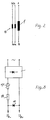
- an amplifier 4 or 5 is connected to each output A or B. of a signal source 1 via a respective resistor 2 or 3.
- These resistors 2, 3 can be part of a surge voltage protection circuit or a radio interference suppression circuit and should not be significantly greater than the internal resistance of the signal source.
- Each of these two amplifiers 4, 5 is designed as an operational amplifier, a potential U A being applied to the non-inverting inputs of the amplifiers 4, 5; both amplifiers are expediently supplied with the same supply voltage U B + and U B -.
- each amplifier has a feedback circuit, which consists of a parallel connection of a diode 6 or 7 and a resistor 8 or 9. The two diodes 6, 7 in the feedback circuits are transparent in the same direction.
- the outputs of the two amplifiers 4, 5 are each connected via a diode 10 or 11 to an input of a signal evaluation circuit 12, which in the present case is a threshold circuit.
- a signal evaluation circuit 12 which in the present case is a threshold circuit.
- This threshold circuit controls a thyristor 13, which in turn controls a consumer 14, which is supplied by a voltage U R1 , U R2 .
- the design of the circuit arrangement according to the invention allows the voltage U a present at the non-inverting inputs of the amplifiers 4, 5 to be advantageously selected only slightly, for example 1.5-2V, more positively than the potential U B - of the supply voltage of the amplifiers 4, 5 can be. Furthermore, the reference voltage U G can be chosen only slightly more negatively than the positive potential U B + of the supply voltage of the amplifiers. In this way, the operating voltage U B -, U B + of the amplifier is used optimally, the amplifiers 5, 6 only having to be controllable in one direction.
- the signal source 1 is formed by the secondary winding 1 'of a summation current transformer 15, as can be seen from FIG. 2.
- the secondary winding 1 'of the converter 15 is connected to the terminals A, B, of the circuit shown in FIG. 1.
- the resistors 2, 3 should have a low resistance, i.e. their resistance values should not be significantly greater than the impedance of the coil 1 '.
- a circuit according to FIG. 3 is expediently provided for the voltage supply of the amplifiers 5, 6.
- a series circuit consisting of a PTC resistor 17 and a resistor 18 is connected to a rectifier 16, so that in conjunction with a voltage limiter circuit, in this case a Zener diode 19, the amplifiers 4, 5 can be supplied with a very different voltage via an AC voltage network.
- the resistance value of the PTC resistor changes due to the resulting increased current flow through the Zener diode Z1, as a result of which the current flow is limited and at the same time the power consumption of the resistors 17, 18 is reduced.
Landscapes
- Engineering & Computer Science (AREA)
- Power Engineering (AREA)
- Physics & Mathematics (AREA)
- General Physics & Mathematics (AREA)
- Amplifiers (AREA)
- Control Of Voltage And Current In General (AREA)
Claims (2)
Applications Claiming Priority (1)
| Application Number | Priority Date | Filing Date | Title |
|---|---|---|---|
| AT260384A AT391559B (de) | 1984-08-10 | 1984-08-10 | Schaltungsanordnung zur auswertung von von einer signalquelle gewonnenen wechselstromsignalen |
Publications (2)
| Publication Number | Publication Date |
|---|---|
| EP0237694A1 EP0237694A1 (fr) | 1987-09-23 |
| EP0237694B1 true EP0237694B1 (fr) | 1989-11-29 |
Family
ID=3537239
Family Applications (1)
| Application Number | Title | Priority Date | Filing Date |
|---|---|---|---|
| EP19860890036 Expired EP0237694B1 (fr) | 1984-08-10 | 1986-02-19 | Agencement de circuit pour l'évaluation de signaux de courant alternatif obtenus à partir d'une source de signal |
Country Status (4)
| Country | Link |
|---|---|
| EP (1) | EP0237694B1 (fr) |
| AT (1) | AT391559B (fr) |
| CH (1) | CH668515A5 (fr) |
| DE (1) | DE3527854C2 (fr) |
Families Citing this family (2)
| Publication number | Priority date | Publication date | Assignee | Title |
|---|---|---|---|---|
| DE3888243D1 (de) * | 1987-06-19 | 1994-04-14 | Festo Kg | Schaltungsanordnung zum Schutz gegen Fehlerströme. |
| FR2698450A1 (fr) * | 1992-11-26 | 1994-05-27 | Balogh Sa | Détecteur de passage inductif. |
Family Cites Families (6)
| Publication number | Priority date | Publication date | Assignee | Title |
|---|---|---|---|---|
| US3546596A (en) * | 1968-06-24 | 1970-12-08 | Sylvania Electric Prod | Absolute value amplifier circuit |
| US4162456A (en) * | 1978-01-10 | 1979-07-24 | Sundstrand Data Control, Inc. | Differential amplifying system |
| US4228475A (en) * | 1978-08-28 | 1980-10-14 | Amf Incorporated | Ground monitoring system |
| DE2838716C3 (de) * | 1978-09-02 | 1981-08-13 | Satchwell Birka Regelungstechnik Gmbh, 5630 Remscheid | Elektrische Schaltungsanordnung zum Betrieb eines mit Wechselspannung gespeisten Elektromotors |
| DE2915703C2 (de) * | 1979-04-12 | 1984-03-29 | Siemens AG, 1000 Berlin und 8000 München | Schaltungsanordnung zur Überwachung der Werte mindestens zweier elektrischer Meßsignale |
| EP0020080A1 (fr) * | 1979-05-29 | 1980-12-10 | Trident Equipment Limited | Dispositifs de protection contre un courant de défaut à la terre |
-
1984
- 1984-08-10 AT AT260384A patent/AT391559B/de not_active IP Right Cessation
-
1985
- 1985-08-02 DE DE19853527854 patent/DE3527854C2/de not_active Expired - Fee Related
- 1985-08-09 CH CH341785A patent/CH668515A5/de not_active IP Right Cessation
-
1986
- 1986-02-19 EP EP19860890036 patent/EP0237694B1/fr not_active Expired
Also Published As
| Publication number | Publication date |
|---|---|
| EP0237694A1 (fr) | 1987-09-23 |
| DE3527854A1 (de) | 1986-02-27 |
| CH668515A5 (de) | 1988-12-30 |
| ATA260384A (de) | 1990-04-15 |
| AT391559B (de) | 1990-10-25 |
| DE3527854C2 (de) | 1993-12-02 |
Similar Documents
| Publication | Publication Date | Title |
|---|---|---|
| DE3141714C2 (fr) | ||
| DE3783348T2 (de) | Leitungsspeiseschaltung mit aktiver impedanz. | |
| DE2642146C2 (de) | Schutzschaltung für ein Leistungselement einer integrierten Schaltung | |
| DE2240538C3 (de) | Stromstabilisierungseinrichtung | |
| DE3521316A1 (de) | Teilnehmeranschlussschaltung mit digitaler signaluebertragung fuer fernsprechanlagen | |
| EP0237694B1 (fr) | Agencement de circuit pour l'évaluation de signaux de courant alternatif obtenus à partir d'une source de signal | |
| DE1176192B (de) | Elektronisches Schaltnetz zum selektiven Verbinden einer ersten oder einer zweiten Klemme mit einer dritten Klemme nach Mass-gabe der momentanen Polaritaet eines Steuersignals | |
| DE2328402A1 (de) | Konstantstromkreis | |
| DE1229601B (de) | Frequenzumsetzer | |
| DE3717591C2 (fr) | ||
| EP0233443B1 (fr) | Agencement de circit pour l'évaluation de signaux de courant alternatif obtenus à partir du secondaire d'un transformateur | |
| DE3013212C2 (fr) | ||
| EP0023683A1 (fr) | Circuit de redresseur en pont | |
| DE1289553B (de) | Elektronischer Schalter mit einer Dioden-Brueckenschaltung | |
| DE69429080T2 (de) | Konstantstromquelle | |
| DE2716038C3 (de) | Phasenschieberschaltung | |
| DE2329579B2 (de) | Quadrier- oder Effektivwertgleichrichter-Schaltung | |
| DE4230977C2 (de) | Schaltungsanordnung zum Gleichrichten einer Wechselspannung | |
| DE903826C (de) | Schaltung mit einem statischen Sekundaerelektronenverstaerker zur Erzielung konstanter Verstaerkung bei Schwankungen der Betriebsspannungen | |
| DE2361806B2 (de) | Linearer Verstärker mit großer Bandbreite und hohem Verstärkungsfaktor auf der Basis von Josephson-Elementen | |
| DE3236148A1 (de) | Schaltungsanordnung zum einstellen der verstaerkung eines verstaerkers | |
| DE3531645A1 (de) | Schaltungsanordnung zum schutz gegen auf signalleitungen auftretenden stoerspannungen | |
| DE2809400A1 (de) | Als nichtlinearer zweipol mit schwellencharakteristik verwendbare schaltungsanordnung und ihre verwendung | |
| DE1234800B (de) | Halbleiteranordnung mit nichtlinearer oder fallender Strom-Spannungscharakteristik | |
| DE1954061C3 (de) | Schaltungsanordnung mit einer von der Kurvenform einer zu überwachenden elektrischen MeßgröBe abhängigen Ansprechempfindlichkeit |
Legal Events
| Date | Code | Title | Description |
|---|---|---|---|
| PUAI | Public reference made under article 153(3) epc to a published international application that has entered the european phase |
Free format text: ORIGINAL CODE: 0009012 |
|
| AK | Designated contracting states |
Kind code of ref document: A1 Designated state(s): FR GB IT |
|
| 17P | Request for examination filed |
Effective date: 19870904 |
|
| 17Q | First examination report despatched |
Effective date: 19871202 |
|
| GRAA | (expected) grant |
Free format text: ORIGINAL CODE: 0009210 |
|
| AK | Designated contracting states |
Kind code of ref document: B1 Designated state(s): FR GB IT |
|
| PG25 | Lapsed in a contracting state [announced via postgrant information from national office to epo] |
Ref country code: IT Free format text: LAPSE BECAUSE OF FAILURE TO SUBMIT A TRANSLATION OF THE DESCRIPTION OR TO PAY THE FEE WITHIN THE PRESCRIBED TIME-LIMIT;WARNING: LAPSES OF ITALIAN PATENTS WITH EFFECTIVE DATE BEFORE 2007 MAY HAVE OCCURRED AT ANY TIME BEFORE 2007. THE CORRECT EFFECTIVE DATE MAY BE DIFFERENT FROM THE ONE RECORDED. Effective date: 19891129 |
|
| GBT | Gb: translation of ep patent filed (gb section 77(6)(a)/1977) | ||
| ET | Fr: translation filed | ||
| PLBE | No opposition filed within time limit |
Free format text: ORIGINAL CODE: 0009261 |
|
| PLBE | No opposition filed within time limit |
Free format text: ORIGINAL CODE: 0009261 |
|
| STAA | Information on the status of an ep patent application or granted ep patent |
Free format text: STATUS: NO OPPOSITION FILED WITHIN TIME LIMIT |
|
| 26N | No opposition filed | ||
| 26N | No opposition filed | ||
| REG | Reference to a national code |
Ref country code: FR Ref legal event code: TP |
|
| PGFP | Annual fee paid to national office [announced via postgrant information from national office to epo] |
Ref country code: FR Payment date: 19960130 Year of fee payment: 11 |
|
| REG | Reference to a national code |
Ref country code: FR Ref legal event code: TP |
|
| PGFP | Annual fee paid to national office [announced via postgrant information from national office to epo] |
Ref country code: GB Payment date: 19960212 Year of fee payment: 11 |
|
| REG | Reference to a national code |
Ref country code: GB Ref legal event code: 732E |
|
| PG25 | Lapsed in a contracting state [announced via postgrant information from national office to epo] |
Ref country code: GB Effective date: 19970219 |
|
| GBPC | Gb: european patent ceased through non-payment of renewal fee |
Effective date: 19970219 |
|
| PG25 | Lapsed in a contracting state [announced via postgrant information from national office to epo] |
Ref country code: FR Effective date: 19971030 |
|
| REG | Reference to a national code |
Ref country code: FR Ref legal event code: ST |