EP0237083B1 - An electric device with an operation indicating lamp - Google Patents
An electric device with an operation indicating lamp Download PDFInfo
- Publication number
- EP0237083B1 EP0237083B1 EP87103705A EP87103705A EP0237083B1 EP 0237083 B1 EP0237083 B1 EP 0237083B1 EP 87103705 A EP87103705 A EP 87103705A EP 87103705 A EP87103705 A EP 87103705A EP 0237083 B1 EP0237083 B1 EP 0237083B1
- Authority
- EP
- European Patent Office
- Prior art keywords
- main frame
- electric device
- indicating lamp
- operation indicating
- lamp according
- Prior art date
- Legal status (The legal status is an assumption and is not a legal conclusion. Google has not performed a legal analysis and makes no representation as to the accuracy of the status listed.)
- Expired - Lifetime
Links
- 239000011347 resin Substances 0.000 claims abstract description 24
- 229920005989 resin Polymers 0.000 claims abstract description 24
- 239000000463 material Substances 0.000 claims abstract description 10
- 238000000034 method Methods 0.000 claims description 3
- 238000004519 manufacturing process Methods 0.000 claims 1
- 238000012856 packing Methods 0.000 abstract description 6
- 229910000679 solder Inorganic materials 0.000 abstract description 4
- 239000007787 solid Substances 0.000 description 3
- 239000000428 dust Substances 0.000 description 1
- 238000012986 modification Methods 0.000 description 1
- 230000004048 modification Effects 0.000 description 1
- 238000000465 moulding Methods 0.000 description 1
Images

Classifications
-
- H—ELECTRICITY
- H05—ELECTRIC TECHNIQUES NOT OTHERWISE PROVIDED FOR
- H05K—PRINTED CIRCUITS; CASINGS OR CONSTRUCTIONAL DETAILS OF ELECTRIC APPARATUS; MANUFACTURE OF ASSEMBLAGES OF ELECTRICAL COMPONENTS
- H05K5/00—Casings, cabinets or drawers for electric apparatus
- H05K5/0091—Housing specially adapted for small components
-
- H—ELECTRICITY
- H05—ELECTRIC TECHNIQUES NOT OTHERWISE PROVIDED FOR
- H05K—PRINTED CIRCUITS; CASINGS OR CONSTRUCTIONAL DETAILS OF ELECTRIC APPARATUS; MANUFACTURE OF ASSEMBLAGES OF ELECTRICAL COMPONENTS
- H05K3/00—Apparatus or processes for manufacturing printed circuits
- H05K3/22—Secondary treatment of printed circuits
- H05K3/28—Applying non-metallic protective coatings
- H05K3/284—Applying non-metallic protective coatings for encapsulating mounted components
-
- Y—GENERAL TAGGING OF NEW TECHNOLOGICAL DEVELOPMENTS; GENERAL TAGGING OF CROSS-SECTIONAL TECHNOLOGIES SPANNING OVER SEVERAL SECTIONS OF THE IPC; TECHNICAL SUBJECTS COVERED BY FORMER USPC CROSS-REFERENCE ART COLLECTIONS [XRACs] AND DIGESTS
- Y10—TECHNICAL SUBJECTS COVERED BY FORMER USPC
- Y10T—TECHNICAL SUBJECTS COVERED BY FORMER US CLASSIFICATION
- Y10T29/00—Metal working
- Y10T29/49—Method of mechanical manufacture
- Y10T29/49002—Electrical device making
- Y10T29/49117—Conductor or circuit manufacturing
- Y10T29/49124—On flat or curved insulated base, e.g., printed circuit, etc.
- Y10T29/4913—Assembling to base an electrical component, e.g., capacitor, etc.
- Y10T29/49146—Assembling to base an electrical component, e.g., capacitor, etc. with encapsulating, e.g., potting, etc.
-
- Y—GENERAL TAGGING OF NEW TECHNOLOGICAL DEVELOPMENTS; GENERAL TAGGING OF CROSS-SECTIONAL TECHNOLOGIES SPANNING OVER SEVERAL SECTIONS OF THE IPC; TECHNICAL SUBJECTS COVERED BY FORMER USPC CROSS-REFERENCE ART COLLECTIONS [XRACs] AND DIGESTS
- Y10—TECHNICAL SUBJECTS COVERED BY FORMER USPC
- Y10T—TECHNICAL SUBJECTS COVERED BY FORMER US CLASSIFICATION
- Y10T29/00—Metal working
- Y10T29/49—Method of mechanical manufacture
- Y10T29/49002—Electrical device making
- Y10T29/49117—Conductor or circuit manufacturing
- Y10T29/49169—Assembling electrical component directly to terminal or elongated conductor
- Y10T29/49171—Assembling electrical component directly to terminal or elongated conductor with encapsulating
Definitions
- This invention relates to an electric device with an operation indicating lamp which may be used with a solid state relay and, more particularly to an improved device which can be easily assembled.
- An electric device which is used for a solid state relay and has a light emitting diode (LED) as an operation indicating lamp is well known.
- the LED is electrically connected to a circuit board and can be seen through an indicating hole disposed in the front cover of a case.
- a packing is interposed between the base of the LED and the front cover.
- the case is filled with a resin material which is injected through an opening in the case. The resin in set to fix the position of the circuit board and the electric components mounted on the board.
- an electric device with an operation indicating lamp comprising a base; a case transversely divisible into a main frame and a case cover, the main frame being fitted to the base and the case cover having an indicating hole; an operation indicating lamp visible through the indicating hole provided in the case cover; and a resin material for fixing the components in the case, the resin material being injected into the space provided by the base and the main frame.
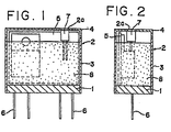
- the device includes a case 2 which is divisible into a main frame 3 and a case cover 4.
- the case 2 is fitted to a base 1 at an open end of the main frame 3.
- a circuit board 5 is electrically connected to a plurality of terminals 6 which protrude from the base 1.
- An LED 7 serving as an operation indicating lamp is electrically connected to the circuit board 5 and visible through an indicating hole 2a of the case cover 4.
- a resin material 8 is injected into the space provided by the base 1 and the main frame 3 and set to fix the circuit board 5 and the components mounted on the board 5.
- the LED 7 is positioned on the board 5 so that the top thereof slightly protrudes from an edge of the board 5 and is electrically connected to the board 5. Then, the board 5 is vertically set and electrically connected to the terminals 6. Subsequently, the main frame 3 is fitted to the base 1 at one open end of the frame 3. The resin material 8 is injected into the space provided by the base 1 and the main frame 3. Finally, the case cover 4 is fitted to the other open end of the main frame 3 so that the LED 7 can be seen through the indicating hole of the case cover 4.
- the resin material 8 does not leak from the indicating hole 2a and the gap between the LED 7 and the indicating hole 2a.
- the LED 7 does not need to be continuously pushed against the case cover 4, preventing cracks from developing in the solder connecting the LED 7 to the circuit board 5 and allowing the easy assembly of the device. Further, because no packings are required for preventing the resin leakage, the LED 7 can be positioned precisely.
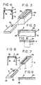
- Figs. 3 through 6 showing an electric device in accordance with a second embodiment of this invention
- guide grooves 4c, 4c on case cover 4 are respectively engaged with guide rails 3c, 3c which are longitudinally provided along the longer edge of the open end of the main frame 3.
- the case cover 4 is slid along the guide rails 3c, 3c to plug the open end of the main frame 3.
- the case cover 4 has a protrusion 4b with which the cover 4 is locked to the open end of the main frame 3 (See Fig. 5).
- the indicating hole 2a is tapered with the inner diameter smaller than the outer one. Because the minimum diameter of the hole 2a is smaller than the diameter of the LED 7, a gap is not developed between the hole 2a and the LED 7 even if the LED is positioned with a deviation from the normal position, preventing foreign matter such as dust from entering.
- the guides 4d, 4d of the case cover 4 are respectively engaged with the guide grooves 3d, 3d provided at the open end of the main frame 3.
- the case cover 4 is slid along the guide grooves 3d, 3d to plug the opening end of the main frame 3.
- the case cover 4 has four locking holes 4e, and the main frame 3 has four locking pieces 3e at the open end.
- the cover 4 is mounted to plug the open end of the main frame 3 by locking the pieces 3e to the holes 4e.
- the indicating hole 2a provided on the cover 4 is tapered with the outer diameter smaller than the inner one. Because the minimum diameter is smaller than the diameter of the LED 7, the LED 7 is positioned by the inner wall of the hole 2a leaving no gap between the LED 7 and the hole 2a.
- a bar 4g disposed on the cover 4 is fixed by the resin, preventing the cover 4 from coming off the main frame 3.
- the cover 4 has four locking pieces 4f, and the main frame 3 has four locking holes 3f at the opening.
- the cover 4 is mounted to plug the open end of the main frame 3 by locking the pieces 4f to the holes 3f.
Landscapes
- Engineering & Computer Science (AREA)
- Microelectronics & Electronic Packaging (AREA)
- Manufacturing & Machinery (AREA)
- Casings For Electric Apparatus (AREA)
- Illuminated Signs And Luminous Advertising (AREA)
- Road Signs Or Road Markings (AREA)
- Circuit Arrangement For Electric Light Sources In General (AREA)
- Push-Button Switches (AREA)
- Devices For Indicating Variable Information By Combining Individual Elements (AREA)
- Lead Frames For Integrated Circuits (AREA)
Priority Applications (1)
| Application Number | Priority Date | Filing Date | Title |
|---|---|---|---|
| AT87103705T ATE79508T1 (de) | 1986-03-14 | 1987-03-13 | Elektrische vorrichtung mit einer betriebsanzeigelampe. |
Applications Claiming Priority (2)
| Application Number | Priority Date | Filing Date | Title |
|---|---|---|---|
| JP37798/86U | 1986-03-14 | ||
| JP1986037798U JPS62149856U (enExample) | 1986-03-14 | 1986-03-14 |
Publications (3)
| Publication Number | Publication Date |
|---|---|
| EP0237083A2 EP0237083A2 (en) | 1987-09-16 |
| EP0237083A3 EP0237083A3 (en) | 1989-10-18 |
| EP0237083B1 true EP0237083B1 (en) | 1992-08-12 |
Family
ID=12507518
Family Applications (1)
| Application Number | Title | Priority Date | Filing Date |
|---|---|---|---|
| EP87103705A Expired - Lifetime EP0237083B1 (en) | 1986-03-14 | 1987-03-13 | An electric device with an operation indicating lamp |
Country Status (5)
| Country | Link |
|---|---|
| US (1) | US4899257A (enExample) |
| EP (1) | EP0237083B1 (enExample) |
| JP (1) | JPS62149856U (enExample) |
| AT (1) | ATE79508T1 (enExample) |
| DE (1) | DE3780987T2 (enExample) |
Cited By (1)
| Publication number | Priority date | Publication date | Assignee | Title |
|---|---|---|---|---|
| DE4407967A1 (de) * | 1994-03-10 | 1995-10-05 | Leuze Electronic Gmbh & Co | Elektronische Vorrichtung |
Families Citing this family (24)
| Publication number | Priority date | Publication date | Assignee | Title |
|---|---|---|---|---|
| US5097592A (en) * | 1989-08-17 | 1992-03-24 | Amp Incorporated | Method of making molded electrical interconnection system |
| JPH07121636B2 (ja) * | 1989-09-27 | 1995-12-25 | 三菱電機株式会社 | 半導体装置カード |
| FR2652941B1 (fr) * | 1989-10-05 | 1993-12-10 | Bull Sa | Piece de fixation multifonctionnelle. |
| US5136460A (en) * | 1990-04-20 | 1992-08-04 | Hubbell Incorporated | Electrical system surge protector |
| US5264661A (en) * | 1991-10-21 | 1993-11-23 | Ford Motor Company | Automotive electronics module |
| US5272594A (en) * | 1992-03-13 | 1993-12-21 | Oneac Corporation | Telephone line overvoltage protection device having aligned, bent terminals supporting a circuit board |
| EP0605712B1 (en) * | 1992-07-17 | 1999-09-08 | Vlt Corporation | Packaging electrical components |
| DE4407782C2 (de) * | 1994-03-09 | 1997-08-28 | Braun Ag | Gehäuse für ein elektrisches Gerät sowie Verfahren zum Einbringen von Vergußmasse in das Gehäuse |
| US5421747A (en) * | 1994-03-28 | 1995-06-06 | The Whitaker Corporation | Connector assembly |
| US5644103A (en) * | 1994-11-10 | 1997-07-01 | Vlt Corporation | Packaging electrical components having a scallop formed in an edge of a circuit board |
| US5945130A (en) * | 1994-11-15 | 1999-08-31 | Vlt Corporation | Apparatus for circuit encapsulation |
| US5728600A (en) * | 1994-11-15 | 1998-03-17 | Vlt Corporation | Circuit encapsulation process |
| US6462265B1 (en) * | 1995-08-15 | 2002-10-08 | Canon Kabushiki Kaisha | Terminal lead-out structure and solar-cell apparatus provided with such structure |
| SE512121C2 (sv) * | 1995-12-19 | 2000-01-31 | Ericsson Telefon Ab L M | Förfarande för att passivt upplinjera ett vågledardon på ett substrat |
| JP3913306B2 (ja) * | 1997-01-21 | 2007-05-09 | キヤノン株式会社 | 太陽電池モジュール |
| DE19844461A1 (de) | 1998-09-28 | 2000-03-30 | Siemens Ag | Hanhabungs- und Montageschutz |
| US6316737B1 (en) | 1999-09-09 | 2001-11-13 | Vlt Corporation | Making a connection between a component and a circuit board |
| US6549409B1 (en) | 2000-08-21 | 2003-04-15 | Vlt Corporation | Power converter assembly |
| US6985341B2 (en) | 2001-04-24 | 2006-01-10 | Vlt, Inc. | Components having actively controlled circuit elements |
| US7443229B1 (en) | 2001-04-24 | 2008-10-28 | Picor Corporation | Active filtering |
| US20060003609A1 (en) * | 2003-09-29 | 2006-01-05 | Tien-Wan Hwang | Fastening structure for memory card |
| JP2007123314A (ja) * | 2005-10-25 | 2007-05-17 | Yazaki Corp | リレーモジュール及び電装ユニット |
| JP2010113842A (ja) * | 2008-11-04 | 2010-05-20 | Fujitsu Component Ltd | 電磁継電器 |
| CN102651443B (zh) * | 2011-02-28 | 2015-01-07 | 展晶科技(深圳)有限公司 | 用于发光二极管封装的导电基板 |
Family Cites Families (9)
| Publication number | Priority date | Publication date | Assignee | Title |
|---|---|---|---|---|
| DE2031395A1 (de) * | 1970-06-25 | 1971-12-30 | Licentia Gmbh | Steuerungsbaugruppe |
| US4028515A (en) * | 1975-09-15 | 1977-06-07 | Illinois Tool Works Inc. | Spring contact switch for dual in line multiple switch assembly having momentary actuated lighted indicators |
| US4054932A (en) * | 1976-02-02 | 1977-10-18 | Square D Company | Over-current protective apparatus for a power circuit |
| US4038584A (en) * | 1976-06-15 | 1977-07-26 | Heinemann Electric Company | Protective arrangement for dependent switching circuits |
| US4172272A (en) * | 1978-05-01 | 1979-10-23 | International Rectifier Corporation | Solid state relay having U-shaped conductive heat sink frame |
| JPS5578418A (en) * | 1978-12-09 | 1980-06-13 | Omron Tateisi Electronics Co | Illumination pushhbutton switch |
| US4361371A (en) * | 1980-12-08 | 1982-11-30 | Amf Incorporated | Packaging of solid state relay |
| DE3048185A1 (de) * | 1980-12-19 | 1982-07-29 | Siemens Ag | Gehaeuse fuer eine gruppe von elektronischen bauelementen |
| JPS59158389U (ja) * | 1983-04-08 | 1984-10-24 | 三菱電機株式会社 | 制御装置 |
-
1986
- 1986-03-14 JP JP1986037798U patent/JPS62149856U/ja active Pending
-
1987
- 1987-03-13 DE DE8787103705T patent/DE3780987T2/de not_active Expired - Lifetime
- 1987-03-13 AT AT87103705T patent/ATE79508T1/de not_active IP Right Cessation
- 1987-03-13 EP EP87103705A patent/EP0237083B1/en not_active Expired - Lifetime
-
1989
- 1989-04-04 US US07/333,865 patent/US4899257A/en not_active Expired - Lifetime
Cited By (1)
| Publication number | Priority date | Publication date | Assignee | Title |
|---|---|---|---|---|
| DE4407967A1 (de) * | 1994-03-10 | 1995-10-05 | Leuze Electronic Gmbh & Co | Elektronische Vorrichtung |
Also Published As
| Publication number | Publication date |
|---|---|
| DE3780987D1 (de) | 1992-09-17 |
| ATE79508T1 (de) | 1992-08-15 |
| EP0237083A3 (en) | 1989-10-18 |
| US4899257A (en) | 1990-02-06 |
| JPS62149856U (enExample) | 1987-09-22 |
| DE3780987T2 (de) | 1993-03-25 |
| EP0237083A2 (en) | 1987-09-16 |
Similar Documents
| Publication | Publication Date | Title |
|---|---|---|
| EP0237083B1 (en) | An electric device with an operation indicating lamp | |
| US5125849A (en) | Connector guide means | |
| US4160576A (en) | Electric power supply connector especially for a fan of the flat type | |
| KR940008442Y1 (ko) | 전도성 각부와 인서어트를 구비한 콘넥터 | |
| US4593221A (en) | Electric motor brush box with stressed opposing walls | |
| US7140885B2 (en) | Housing case for electronic circuit board | |
| KR910003908Y1 (ko) | 전기 접속기 | |
| EP1005109A2 (en) | Electronic control unit with electrical connector | |
| EP0113238B1 (en) | Assembling construction of electronic apparatus | |
| EP0765010A2 (en) | Anti-wicking board to board connector | |
| US5391088A (en) | Surface mount coupling connector | |
| KR970001032Y1 (ko) | 전기 접속기용 가이드 장치 | |
| US3429980A (en) | Electronic component package and cover | |
| KR19990029558A (ko) | 표면실장부품의 형성방법 | |
| US5655042A (en) | Molded slotted optical switch structure and method | |
| US6120324A (en) | Waterproof connector | |
| CN214384726U (zh) | 一种组合式互感器 | |
| KR101786334B1 (ko) | 조인트 커넥터 | |
| US6356454B1 (en) | Electrical unit having an aligning element | |
| KR101733232B1 (ko) | 백커버의 역삽입이 방지된 번인보드 지지대 | |
| KR890002367Y1 (ko) | 릴레이 조립체와 그 제조방법 | |
| JPH0285880A (ja) | 電子機器の表示装置 | |
| KR102681513B1 (ko) | 전자부품의 제조 방법 및 전자부품 | |
| CN223957781U (zh) | 显示屏防水盒及包括其的净水机 | |
| KR102494808B1 (ko) | 직류 전자식 스위치 장치 |
Legal Events
| Date | Code | Title | Description |
|---|---|---|---|
| PUAI | Public reference made under article 153(3) epc to a published international application that has entered the european phase |
Free format text: ORIGINAL CODE: 0009012 |
|
| 17P | Request for examination filed |
Effective date: 19870313 |
|
| AK | Designated contracting states |
Kind code of ref document: A2 Designated state(s): AT BE CH DE ES FR GB GR IT LI LU NL SE |
|
| PUAL | Search report despatched |
Free format text: ORIGINAL CODE: 0009013 |
|
| AK | Designated contracting states |
Kind code of ref document: A3 Designated state(s): AT BE CH DE ES FR GB GR IT LI LU NL SE |
|
| 17Q | First examination report despatched |
Effective date: 19911115 |
|
| GRAA | (expected) grant |
Free format text: ORIGINAL CODE: 0009210 |
|
| AK | Designated contracting states |
Kind code of ref document: B1 Designated state(s): AT BE CH DE ES FR GB GR IT LI LU NL SE |
|
| PG25 | Lapsed in a contracting state [announced via postgrant information from national office to epo] |
Ref country code: SE Free format text: THE PATENT HAS BEEN ANNULLED BY A DECISION OF A NATIONAL AUTHORITY Effective date: 19920812 Ref country code: NL Effective date: 19920812 Ref country code: LI Effective date: 19920812 Ref country code: GR Free format text: LAPSE BECAUSE OF FAILURE TO SUBMIT A TRANSLATION OF THE DESCRIPTION OR TO PAY THE FEE WITHIN THE PRESCRIBED TIME-LIMIT Effective date: 19920812 Ref country code: CH Effective date: 19920812 Ref country code: BE Effective date: 19920812 Ref country code: AT Effective date: 19920812 |
|
| REF | Corresponds to: |
Ref document number: 79508 Country of ref document: AT Date of ref document: 19920815 Kind code of ref document: T |
|
| ITF | It: translation for a ep patent filed | ||
| REF | Corresponds to: |
Ref document number: 3780987 Country of ref document: DE Date of ref document: 19920917 |
|
| REG | Reference to a national code |
Ref country code: CH Ref legal event code: PL |
|
| PG25 | Lapsed in a contracting state [announced via postgrant information from national office to epo] |
Ref country code: ES Free format text: LAPSE BECAUSE OF FAILURE TO SUBMIT A TRANSLATION OF THE DESCRIPTION OR TO PAY THE FEE WITHIN THE PRESCRIBED TIME-LIMIT Effective date: 19921123 |
|
| EN | Fr: translation not filed | ||
| PG25 | Lapsed in a contracting state [announced via postgrant information from national office to epo] |
Ref country code: FR Effective date: 19921231 |
|
| NLV1 | Nl: lapsed or annulled due to failure to fulfill the requirements of art. 29p and 29m of the patents act | ||
| PLBI | Opposition filed |
Free format text: ORIGINAL CODE: 0009260 |
|
| PG25 | Lapsed in a contracting state [announced via postgrant information from national office to epo] |
Ref country code: GB Effective date: 19930313 |
|
| 26 | Opposition filed |
Opponent name: LEUZE ELECTRONIC GMBH + CO Effective date: 19930127 |
|
| PG25 | Lapsed in a contracting state [announced via postgrant information from national office to epo] |
Ref country code: LU Free format text: LAPSE BECAUSE OF NON-PAYMENT OF DUE FEES Effective date: 19930331 |
|
| GBPC | Gb: european patent ceased through non-payment of renewal fee |
Effective date: 19930313 |
|
| REG | Reference to a national code |
Ref country code: FR Ref legal event code: ST |
|
| PLBO | Opposition rejected |
Free format text: ORIGINAL CODE: EPIDOS REJO |
|
| PLBN | Opposition rejected |
Free format text: ORIGINAL CODE: 0009273 |
|
| STAA | Information on the status of an ep patent application or granted ep patent |
Free format text: STATUS: OPPOSITION REJECTED |
|
| 27O | Opposition rejected |
Effective date: 19960309 |
|
| PG25 | Lapsed in a contracting state [announced via postgrant information from national office to epo] |
Ref country code: IT Free format text: LAPSE BECAUSE OF NON-PAYMENT OF DUE FEES;WARNING: LAPSES OF ITALIAN PATENTS WITH EFFECTIVE DATE BEFORE 2007 MAY HAVE OCCURRED AT ANY TIME BEFORE 2007. THE CORRECT EFFECTIVE DATE MAY BE DIFFERENT FROM THE ONE RECORDED. Effective date: 20050313 |
|
| PGFP | Annual fee paid to national office [announced via postgrant information from national office to epo] |
Ref country code: DE Payment date: 20060331 Year of fee payment: 20 |