EP0231237B1 - Systeme de commande pour modules de circuits en chaine - Google Patents
Systeme de commande pour modules de circuits en chaine Download PDFInfo
- Publication number
- EP0231237B1 EP0231237B1 EP86904286A EP86904286A EP0231237B1 EP 0231237 B1 EP0231237 B1 EP 0231237B1 EP 86904286 A EP86904286 A EP 86904286A EP 86904286 A EP86904286 A EP 86904286A EP 0231237 B1 EP0231237 B1 EP 0231237B1
- Authority
- EP
- European Patent Office
- Prior art keywords
- module
- modules
- data
- control system
- shift register
- Prior art date
- Legal status (The legal status is an assumption and is not a legal conclusion. Google has not performed a legal analysis and makes no representation as to the accuracy of the status listed.)
- Expired - Lifetime
Links
- 230000006870 function Effects 0.000 claims description 12
- 230000004044 response Effects 0.000 claims description 5
- 230000001419 dependent effect Effects 0.000 claims description 3
- 238000012545 processing Methods 0.000 claims description 3
- 101100421141 Homo sapiens SELENON gene Proteins 0.000 abstract description 21
- 102100023781 Selenoprotein N Human genes 0.000 abstract description 21
- BSFODEXXVBBYOC-UHFFFAOYSA-N 8-[4-(dimethylamino)butan-2-ylamino]quinolin-6-ol Chemical compound C1=CN=C2C(NC(CCN(C)C)C)=CC(O)=CC2=C1 BSFODEXXVBBYOC-UHFFFAOYSA-N 0.000 abstract description 16
- 101000622123 Homo sapiens E-selectin Proteins 0.000 abstract description 16
- 101150012612 SELENOW gene Proteins 0.000 abstract description 11
- 101150105184 Selenos gene Proteins 0.000 abstract description 9
- 238000012360 testing method Methods 0.000 description 11
- 238000010586 diagram Methods 0.000 description 7
- 238000000034 method Methods 0.000 description 5
- 230000003111 delayed effect Effects 0.000 description 4
- 230000000295 complement effect Effects 0.000 description 3
- 238000006073 displacement reaction Methods 0.000 description 3
- 238000010200 validation analysis Methods 0.000 description 3
- 230000007547 defect Effects 0.000 description 2
- 230000000694 effects Effects 0.000 description 2
- 238000009432 framing Methods 0.000 description 2
- 230000002093 peripheral effect Effects 0.000 description 2
- 238000013459 approach Methods 0.000 description 1
- 238000004891 communication Methods 0.000 description 1
- 238000013461 design Methods 0.000 description 1
- 238000011161 development Methods 0.000 description 1
- 239000012634 fragment Substances 0.000 description 1
- 238000013101 initial test Methods 0.000 description 1
- 230000010354 integration Effects 0.000 description 1
- 230000000717 retained effect Effects 0.000 description 1
- 238000012546 transfer Methods 0.000 description 1
Images


Classifications
-
- G—PHYSICS
- G11—INFORMATION STORAGE
- G11C—STATIC STORES
- G11C11/00—Digital stores characterised by the use of particular electric or magnetic storage elements; Storage elements therefor
- G11C11/21—Digital stores characterised by the use of particular electric or magnetic storage elements; Storage elements therefor using electric elements
- G11C11/34—Digital stores characterised by the use of particular electric or magnetic storage elements; Storage elements therefor using electric elements using semiconductor devices
- G11C11/40—Digital stores characterised by the use of particular electric or magnetic storage elements; Storage elements therefor using electric elements using semiconductor devices using transistors
- G11C11/401—Digital stores characterised by the use of particular electric or magnetic storage elements; Storage elements therefor using electric elements using semiconductor devices using transistors forming cells needing refreshing or charge regeneration, i.e. dynamic cells
- G11C11/406—Management or control of the refreshing or charge-regeneration cycles
-
- G—PHYSICS
- G11—INFORMATION STORAGE
- G11C—STATIC STORES
- G11C29/00—Checking stores for correct operation ; Subsequent repair; Testing stores during standby or offline operation
- G11C29/006—Checking stores for correct operation ; Subsequent repair; Testing stores during standby or offline operation at wafer scale level, i.e. wafer scale integration [WSI]
-
- G—PHYSICS
- G11—INFORMATION STORAGE
- G11C—STATIC STORES
- G11C7/00—Arrangements for writing information into, or reading information out from, a digital store
-
- G—PHYSICS
- G11—INFORMATION STORAGE
- G11C—STATIC STORES
- G11C7/00—Arrangements for writing information into, or reading information out from, a digital store
- G11C7/22—Read-write [R-W] timing or clocking circuits; Read-write [R-W] control signal generators or management
-
- G—PHYSICS
- G11—INFORMATION STORAGE
- G11C—STATIC STORES
- G11C8/00—Arrangements for selecting an address in a digital store
-
- G—PHYSICS
- G11—INFORMATION STORAGE
- G11C—STATIC STORES
- G11C8/00—Arrangements for selecting an address in a digital store
- G11C8/12—Group selection circuits, e.g. for memory block selection, chip selection, array selection
-
- G—PHYSICS
- G11—INFORMATION STORAGE
- G11C—STATIC STORES
- G11C8/00—Arrangements for selecting an address in a digital store
- G11C8/18—Address timing or clocking circuits; Address control signal generation or management, e.g. for row address strobe [RAS] or column address strobe [CAS] signals
Definitions
- the present invention relates to a control system for chained circuit modules. It is known to connect a plurality of circuit modules in a chain, each module being capable of performing some memory and/or data processing operation.
- the circuit modules may be undiced chip areas of an integrated circuit wafer and the chain of modules may be grown by actuation of electronic switching functions within the modules, as described in GB 1 377 859.
- the chain may be single (and approximate a spiral) or may be branched.
- a module may be regarded as composed of a function unit, which performs the memory or data processing operation proper of the unit, and control logic which responds to commands.
- Various techniques have been suggested for addressing commands to individual modules. Each module may be given its own address and commands can include address fields, whereby associative addressing is employed.
- GB 1 377 859 Another idea proposed in GB 1 377 859 is to issue a global command to all modules. Such a command is issued by way of a global line, that is to say a line running to all modules in parallel, in contrast to lines chained through the modules. Other global lines can include power and clock lines.
- a module performs a specific function when it receives the global command and the module is concurrently receiving a specific state signal from an adjacent module.
- this is proposed as part of the mechanism for growing the chain of modules. It is of extremely limited application, enabling one particular command to be sent only to the end of the chain. In use of the chain of modules, it is obviously necessary to be able to address various commands to modules anywhere along the chain.
- serial logic An important consideration in the case of chained modules is the integrity of the chaining paths between modules. These include part of the control logic of each module and this part will be called the serial logic.
- the control logic will additionally include side-chain logic, that is to say logic which is branched off the path through which the modules are chained. Any defect in the serial logic of a module will break the chain and render the apparatus inoperable. Particularly when the modules are undiced chip areas, i.e. parts of a wafer scale integration (WSI) system, there is a high premium on keeping the serial logic as simple as possible. As is well known, a significant problem in WSI is avoidance of faulty modules.
- WSI wafer scale integration
- serial logic of a faulty module provides the serial logic is functioning
- the function unit of the module is not used, and may even be disabled, because it is faulty.
- the use of good serial logic of otherwise faulty modules makes it possible to grow chains more efficiently and include within the chain a higher proportion of non-faulty modules than if the chain excludes a module which is in any way faulty, (which is the approach adopted in GB 1 377 859).
- the object of the present invention is to provide a control system which enables flexible addressing to be achieved using relatively simple control logic.
- a more specific object of the preferred implementation of the invention is to enable flexible addressing to be achieved with extremely simple serial logic.
- each module includes a shift register arrangement responsive to clock pulses (WCK) provided to all modules in the chain, each module includes serial logic forming part of the chaining path, and all the modules are connected to a global command line (CMND) characterised in that the serial logic includes at least one shift register stage of the shift register arrangement, a token bit is launched into the chain of modules and clocked from module to module along the serial logic, each module being operative to execute a selected one of the repertoire of commands in response to a command signal received on the global command line (CMND) and the coincident presence of a token bit (T-BIT) received through the preceding modules in the chain and injected into its shift register arrangement, the command selection being at least partially determined by the position of the token bit in the shift register arrangement on termination of the command signal.
- CMND global command line
- the token could consist of more than one bit and the selection of a command could then be determined in part by the location of the token and in part by a decode of the token itself.
- a single bit token such as a "1" in a stream of zeroes
- command selection dependent solely upon the location of the token when the global command signal is received Further description will proceed in accordance with use of a single bit token, i.e. a token bit.
- each module can include an m-bit shift register in its serial logic.
- a token bit is launched down the chain of modules and, after (i x m) + j clock pulses the token bit will be in the j th command bit of the i th module.
- the global command is then issued to all modules. Because of the location of the token bit, the i th module executes the j th command.
- the above implementation suffers from two drawbacks.
- the shift register arrangement is mainly or wholly in the side-chain logic.
- the serial logic includes very few, preferably only one, bit buffer stages.
- Two global command signals are now required. The first causes a token to be seized at a module and to be clocked down its side-chain shift register arrangement. The second causes the module in question to execute a command in dependence upon the position which the token has reached along the side-chain shift register arrangement.
- the first and second global command signals could be provided by way of separate global lines but it is much preferred to use a single global line and to provide both signals on this line.
- the preferred technique is to represent one signal by asserting a particular logic level and to represent the second signal by terminating this assertion. In the embodiment to be described below the first signal is given when CMND goes true, the second when CMND reverts to false.
- a token When a token is seized at a module it may be arrested in that module until the second signal, when it may be allowed to proceed to more remote modules; this is the option selected in the embodiment described below. Alternatively the token may be seized "on the fly" and be allowed to continue on its way for use on a subsequent assertion of the first signal.
- the latency in executing the j th command at the i th module is only i + j clock pulses.
- Fig 1 shows a few modules 10 on a wafer which may contain a few hundred modules arranged on the wafer.
- the modules are set in a grid of global lines, namely a V DD power line 11, a V SS power line 12, a WCK (wafer clock) line 13 and a CMND (command) line 14. All these lines go to bondsites on the edge of the wafer or WCK and CMND may go to a command module on the wafer.
- Fig 2 shows the same modules 10 minus the global lines but with inter-module lines 15 for transmit paths.
- Data may be sent through a chain of modules, starting at a bondsite identified as XMIT (transmit; not shown).
- the modules have four connections into their XMIT path and these connections are identified as follows:
- the modules have four connections out from their XMIT paths and these connections are identified as follows:
- these output lines are switched so that a module can select only one of its edge neighbours as the next module in the chain, on to which XMIT data is passed.
- the modules are also connected by receive path inter-module lines 16 (Fig 3) which allow data to be sent back to a bondsite identified as RECV (not shown).
- the modules have four connections into their RECV paths:
- the modules have four connections out of their RECV paths:
- the XOUT and RIN selections are effected by four selection signals SELN, SELE, SELS and SELW, whose generation is explained below. Only one of these signals can be true. If SELN is true, for example, the module routes the XMIT path to the adjacent module above and accepts RECV data from that module.
- the SEL signals of the modules are set up basically as described in GB 1 377 859. Modules are added one by one to the chain, tested and retained if good, and the procedure is reiterated to grow a chain of interconnected modules.
- the chain tends to spiral in to the centre of the wafer in the case of a peripheral bondsite for XMIT and RECV. There may be a plurality of such bondsites, say four, to improve the chance of finding a good place to start the chain.
- the testing is effected in stages in the present system, as described further below.
- Fig 4 illustrates a peripheral fragment 17 of a wafer with modules 10 and the bondsite terminals XMIT and RECV. Portions of the XMIT path and RECV path are shown in full and broken lines respectively, as they would be grown through modules in accordance with the algorithm that each module tries its selection options in the order SELN, SELE, SELS and SELW.
- the first module M1 fails with SELN (there is no module above it) but succeeds with SELE, so adding M2 to the chain.
- M2 succeeds with SELN and adds M3.
- M3 fails with SELN but succeeds with SELE, to add M4.
- M5 succeeds with SELN to add M5, and so on. In the example shown all modules are good, at least so far as their control logic is concerned.
- the module Normally the module merely acts as a link in the chain and outbound data and commands pass from XMIT through the XMIT path in the module with a 1-bit delay through each module. Inbound data returns to RECV through the RECV path in the module, also with a 1-bit delay through each module.
- Each module contains a 16 k x 1 bit dynamic RAM unit which is constantly refreshed under control of a free-running address counter.
- the module also contains control logic which can respond to commands to effect SELN, SELE, SELS and SELW and to other commands of which the most important are READ and WRITE.
- the chain is broken at that module and the RAM unit is written to in the case of WRITE and read from in the case of READ.
- the RAM unit is composed of random access blocks it is only addressed by the free running counter and treated as a 16k block of serial memory. In a READ operation, all 16k of memory are read out on to the RECV line.
- the memory block will be read out correctly starting from address O and running through to address (216 - 1). If the READ command is not thus timed, the data will be "wrapped round" - in an address order N, ..., (216 - 1), O, ..., (N-1) where N is the address obtaining at the READ command.
- the data can be accepted in this order at RECV and then cyclically shifted to establish the correct address order.
- a WRITE operation 16k of data is written from XMIT into the RAM unit.
- the command and ensuing data can either be correctly timed in relation to the address counter cycle or can be pre-wrapped-round to match the address N at which the write starts.
- Another possibility is to write regardless and store the value in the address counter cycle marking the start of the written block, this stored value being used when the block is read to enable it to be correctly unwrapped.
- OFFSET gives the number in the module's address counter at a datum address cycle time, corrected to take account of the time taken to access the module (1-bit delay through each preceding module).
- FLAG is a single bit which indicates whether the RAM unit of the module is usable.
- OFFSET it is not essential to know OFFSET. If a data block includes a suitable framing word 16k blocks may be written and read without regard to wrap-round. After reading a block it may be "unwrapped" by finding the framing word.
- Fig 5 is a block diagram of one module.
- the four XIN terminals merge into XIN which forms the input to XMIT PATH LOGIC 20, within which the switching takes place to route the XMIT path to XOUTN, XOUTE, XOUTS or XOUTW.
- the four RIN terminals enter RECV PATH LOGIC 21 which selects one RIN terminal for connection to ROUT which branches to the four ROUT terminals.
- XIN is also connected to CON LOGIC 22 (configuration logic) which decodes commands and provides the above-mentioned selection signals SELN, SELE etc and other commands, including READ and WRITE commands for a RAM UNIT 23.
- the command line CMND is fed to a clocked buffer 24 which provides complementary signals CMND (designating command mode) and CMND BAR (designating "transmit mode").
- CMND designating command mode
- CMND BAR designating "transmit mode”
- transmit mode the module acts simply as a link in the chain passing on both outward bound XMIT path data and inward bound RECV path data.
- command mode the module detects whether a command token is present in its XMIT path logic and, if it is, decodes and obeys the command addressed thereto, i.e. timed to provide a token bit in that module when CMND goes true.
- CMND, CMND BAR and signals in general are gated with clock signals (described below) as is conventional in MOS circuits. For simplicity this design detail is ignored in the present description.
- the buffer 24 also detects a global reset signal (CMND true for just one clock period) and generates an internal initialization signal INIT BAR (i.e. initialization asserted when the signal is false). This is readily detected by logic which generates INIT BAR in response to the state sequence TMODE, CMODE, TMODE in successive clock periods.
- the initialization is global because INIT BAR is generated by every module, regardless of what is received at XIN along the XMIT path itself. The use of global reset is described below.
- the function unit of the module is a 16k RAM UNIT 23.
- WRITE 16k of data from the XMIT PATH LOGIC 20 is written into the RAM UNIT via a line RID (RAM input data).
- READ 16k of data is passed to the RECV PATH LOGIC 21 via a line ROD (RAM output data).
- a timing pulse generator 25 provides multiphase timing pulses PHASE CLOCKS in response to WCK. Although PHASE CLOCKS are shown connected only to CON LOGIC 22, they are of course distributed to the module circuits generally.
- a module has seven mutually exclusive states as follows:
- the CON LOGIC also provides a signal RPON (RAM power on) to switch on the RAM power supply.
- RPON is reset by INIT BAR and can be toggled by a command addressed to a module.
- Another command provides a strobe ACR (address counter reset) to the RAM UNIT 23 to reset its address counter at the instant of the strobe.
- the RAM UNIT 23 is not essential to the operation of a module as a link in a chain. It can be independently switched on and off by means of RPON. Thus the chain of "good" modules can be grown having regard to the operability of the control logic 20, 21, 22, 24, 25. If a module is encountered with bad control logic, the chain will have to be retracted and a new module in a different direction tried. This will be the situation at the edge of the wafer; a non-existent module will inevitably appear to be bad.
- the control logic is permanently connected to the power lines but is of small area and defects are unlikely to affect infer yield much. However the RAM UNIT, if faulty, could draw heavy current and collapse the voltage on the power tracks 11 and 12 to which it is connected, so affecting large numbers of neighbouring modules.
- the RAM data inputs are connected to the common input line RID (RAM input data) which accepts data from the XMIT PATH LOGIC.
- the RAM sense amplifiers 34 are connected to the common output line ROD (RAM output data) which passes data to the RECV PATH LOGIC.
- the detailed management of the RAM's is effected conventionally by a clock generator 35 which receives the PHASE CLOCKS, READ and WRITE and effects precharge, discharge, refresh and so on, in a manner which need not be described here.
- the counter 33 comprises a 7-bit column counter (least significant half) and a 7-bit row counter (most significant half). Every time a carry propagates from the column counter to the row counter, a signal REFR is given to the clock generator 35 and the currently addressed row is refreshed in well known manner. Thus refresh takes place every 128 (27) clock pulses and a cycle of 128 x 128 clock pulses is required to refresh all rows of the RAM blocks 32.
- ACR ACR Activated Cell Reduction
- the address counter carry bit is denoted ACCO (address counter carry out) and this may also be utilized in one test facility to be described below.
- Fig 7 is a detailed diagram of the XMIT PATH LOGIC 20.
- XIN is connected through an FET 40 enabled by CMND BAR to a clocked 1-bit stage 41, from which drive is provided to the XOUT lines.
- Each such line includes a first FET 46 which is normally enabled by a validation latch 47 and a second FET 48 of which only one is enabled by the corresponding signal SELN, SELE, SELS or SELW.
- the validation latch 47 provides a safety feature.
- the CON LOGIC asserts a reset signal RESET BAR which resets any SEL signal which is set. Failure for this to take place is a recipe for disaster.
- XIN is connected to one of XOUTN, XOUTE, XOUTS, XOUTW through FET 40, 1-bit stage 41, one of the FETs 46 and whichever of the FETs 48 is enabled.
- CMND BAR is again asserted and the data passes through the FET 40 and 1-bit stage 41 to RID.
- the output of the 1-bit stage 41 is fed back to the input of the stage through an FET 49 which is enabled by CMND to form a 1-bit latch which latches the bit therein at the time CMND is asserted.
- This output is XPLO (transmit path latch out), which is physically the same as RID.
- XPLO is what tells the CON LOGIC 22 whether the module in question is addressed or not when CMND is asserted.
- Fig 8 shows the RECV PATH LOGIC 21.
- RINN, RINE, RINS and RINW are connected through respective FET's 50 to a node 51.
- the FETs 50 are enabled by SELN, SELE, SELS and SELW respectively.
- the node 51 is connected through an FET 52 enabled by HOLD and a clocked 1-bit stage 53 to ROUT.
- HOLD will be explained below but, for understanding of Fig 8 it suffices to know that it is true consequent on CMND BAR is true, so that the module is established as a link in the chain, connecting the correct one of RINN to RINW to ROUT.
- ROD is connected to the input of the 1-bit stage 53 through an FET 55 enabled by READ.
- a terminal TEST is connected to the input of the 1-bit stage 53 through an FET 56 enabled by WRITE.
- TEST may be connected to RID (Fig 7) so that when a write operation is performed, the data sent to the module in question along the XMIT path is returned from that module along the RECV path. The returned data can then be checked against the transmitted data. This may be useful as part of data vertification procedures during normal use of the configured wafer.
- TEST is implemented by connecting it to ACCO (Fig 6). Then, during a write operation, a pulse should be injected into the RECV path every 16k clock pulses. This may be useful to test the address counter 33 during the initial configuration procedures.
- a further test facility to be explained below is provided by a terminal SCAN OUT connected to the input to the 1-bit stage 53 through an FET 57 which is enabled by a signal SHIFT which is complementary to HOLD.
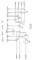
- Fig 9 shows one part of this circuit which generates the above mentioned signals RESET BAR, HOLD and SHIFT and a signal TBIT which is a token bit to be shifted along a shift register described with reference to Fig 10.
- XIN is connected through a FET 60 enabled by CMND BAR to a 1-bit stage 61.
- WRITE and READ are also connected to the stage 61 which performs an OR function.
- the output of the 1-bit stage 61 is gated in a NAND gate 62 with CMND to provide RESET BAR which is also provided in response to INIT BAR by an AND gate 63.
- the output of the 1-bit stage 61 is buffered for one more bit time by a stage 64 to provide TBIT (token bit) which is a bit to be clocked down the shift register (Fig 10) so long as CMND is asserted.
- TBIT token bit
- RESET BAR can only be asserted and TBIT generated when (1) the transmit path latch 41 contains a 1-bit when CMND is asserted or (2) READ or WRITE is asserted when CMND is raised, irrespective of the contents of the transmit path latch.
- Case (1) represents the normal way of addressing a command to a module: asserting CMND at the time a 1-bit is present in the module on the XMIT path.
- Case (2) provides a means of aborting a WRITE or READ operation.
- XPLO will be latched at 1 in an addressed chip.
- XPLO is applied to a 1-bit stage 67 through an FET 66 enabled by CMND to provide SHIFT which enables the abovementioned shift register in order to clock TBIT along the register until CMND ceases to be asserted, and complementary signal HOLD.
- XPLO is one bit delayed relative to XIN and SHIFT is a further bit delayed relative to XPLO.
- RESET BAR is one bit delayed relative to CMND and TBIT is a further bit delayed. RESET BAR is thus generated off the same bit as is latched to form XPLO and one bit later, this same bit appears as TBIT to be clocked along the shift register with SHIFT true.
- Fig 10 shows the remainder of the CON LOGIC 22, consisting of a chain of eight clocked D-type flip-flops 70-77 forming the shift register and a T-type flip-flop 78.
- the passage of signals is controlled by gates symbolically represented by small strokes with an adjacent S, meaning enabled by SHIFT or an adjacent H, meaning enabled by HOLD.
- the flip-flops 70 to 75 provide SELN, SELE, SELS, SELW, READ and WRITE respectively. Assuming that the module in question is addressed it can be seen that these six flip-flops will first be cleared by RESET BAR. Then TBIT will be clocked from flip-flop to flip-flop for as long as SHIFT remains true. When SHIFT becomes false and HOLD becomes true, which is when CMND goes false, the TBIT is latched in whichever flip flop it has reached.
- SCAN OUT is injected into the RECV path as described with reference to Fig 8 and can be detected at the RECV terminal.
- the provision of SCAN OUT is a demonstration that the CON LOGIC 22 (excluding the flip-flop 78) is functioning. Accordingly it is satisfactory to use the module in the chain of modules, whether or not its RAM UNIT is functional.
- This flip-flop provides RPON and is reset by the global initialization signal INIT BAR.
- the first module M1 (Fig 4) is then tested with n greater than 9 and if SCAN OUT is detected back at RECV, all is well. If not another M1 must be selected and for this purpose there are say four XMIT, RECV bondsites around the periphery of the wafer connected to different modules.
- n 2 to latch SELN.
- M2 is tested with n greater than 9 and SCAN OUT appears.
- the module address table is built up to record for each module what its selection direction is.
- the command resets SELE so the chain connected to XMIT again consists of M1 only although the more remote part of the chain remains in tact.
- Fig 11 shows the control circuitry for controlling the addressing of the modules.
- This circuitry may be off the wafer and interfaces with a control processor (not shown) which provides the necessary data and a strobe signal ENABLE which initiates a command operation.
- This processor stores the aforementioned table to enable it to time ENABLE and SERIAL DATA correctly.
- ENABLE When ENABLE goes true (see also Fig 12) it generates a 1-bit TOKEN via flip-flops D1 and D2, whose outputs QD1 and QD2 BAR are shown in Fig 12, and an AND gate A1.
- the TOKEN is applied to XMIT via a multiplexer 80.
- ENABLE also enables (EN terminal) a 9-bit displacement counter A2 which is used to count the number of clock pulses to the module to be addressed.
- a 9-bit counter will handle a chain of up to 512 modules.
- the counter 81 will have been preset by the control processor with the correct initial value denoted DISPLACEMENT DATA and, when enabled, counts clock pulses WCK until a terminal count BD is reached.
- BD is latched in a latch L1 whose output QL1 enables a second counter 82 and also initiates CMND via an AND gate 82.
- the counter 82 is a 4-bit command counter preset in accordance with the desired duration of CMND by CMND DATA. When this counter reaches its terminal count BC a second latch L2 latches BC and the QL2 BAR output of this latch disables the gate A2, so terminating CMND.
- QL2 BAR may be used to reset the latches D1, D2, L1, L2.
- the controlling processor When a WRITE command is set up, the controlling processor must feed the serial data to XMIT after CMND has gone low again and in doing this it applies a signal WRITE SEL to the multiplexer 80 to connect SERIAL WRITE DATA to XMIT.
- the controlling processor When a READ command is set up, the controlling processor must be ready to accept serial read data from RECV m clock pulses after the termination of CMND, where m corresponds to the displacement of the addressed module from RECV.
- CMND When there is only a single TOKEN bit on the XMIT path. If more than one bit is on the path, multiple addressing will occur, with the same command given to all addressed modules, because this is determined by the duration of CMND.
- a single TOKEN bit can be used to address a plurality of modules in sequence. The bit is latched in the latch 41, 42 (Fig 7) and, when a command is terminated at one module, can continue to another module, which is addressed when CMND is asserted, provided the one module is in a state with one of its SEL signals asserted.
- TPC TERMINATION WITH PATH CLOSURE
- the XMIT path latch of the target module contains a '0' when the CMND line is raised at the end of the READ or WRITE operation. Raising the CMND line resets the shift-register, terminating the current operation.
- TOA there is no command token present to generate an onward path.
- TPC will be used with a command token set at some module nearer XMIT so that, when CMND is raised, a new path will be configured from THAT chip, or a read or write operation will be set up there.
- ABORT If CMND is raised at any time prior to the end of a complete read or write operation, that operation will immediately be terminated.
- a graceful ABORT from a READ operation may be made by ensuring that the XMIT path is flushed with '0's prior to the abort.
- a TOA- or TPC-like ABORT prior to the end of a READ operation is possible by injecting a single '1' into the flushed XMIT path. It is more difficult to abort a WRITE operation gracefully as multiple module addressing will generally occur due to the presence of multiple '1's in the XMIT path write data stream when CMND is raised.
Landscapes
- Engineering & Computer Science (AREA)
- Microelectronics & Electronic Packaging (AREA)
- Computer Hardware Design (AREA)
- Static Random-Access Memory (AREA)
- Semiconductor Integrated Circuits (AREA)
- Oscillators With Electromechanical Resonators (AREA)
- Storage Device Security (AREA)
- Memory System (AREA)
- Exchange Systems With Centralized Control (AREA)
- Use Of Switch Circuits For Exchanges And Methods Of Control Of Multiplex Exchanges (AREA)
- Tests Of Electronic Circuits (AREA)
- Vehicle Body Suspensions (AREA)
- Control Of Stepping Motors (AREA)
- Amplifiers (AREA)
- Iron Core Of Rotating Electric Machines (AREA)
- Crystals, And After-Treatments Of Crystals (AREA)
- Dram (AREA)
- Time-Division Multiplex Systems (AREA)
- For Increasing The Reliability Of Semiconductor Memories (AREA)
- Non-Volatile Memory (AREA)
- Semiconductor Memories (AREA)
Claims (21)
Priority Applications (1)
| Application Number | Priority Date | Filing Date | Title |
|---|---|---|---|
| AT86904286T ATE67890T1 (de) | 1985-07-12 | 1986-07-11 | Steuersystem fuer gekettete schaltungsmodule. |
Applications Claiming Priority (2)
| Application Number | Priority Date | Filing Date | Title |
|---|---|---|---|
| GB8517699 | 1985-07-12 | ||
| GB8517699A GB2177825B (en) | 1985-07-12 | 1985-07-12 | Control system for chained circuit modules |
Related Child Applications (1)
| Application Number | Title | Priority Date | Filing Date |
|---|---|---|---|
| EP19900202616 Division-Into EP0416714A3 (en) | 1985-07-12 | 1986-07-11 | Wafer-scale integrated memory circuits |
Publications (2)
| Publication Number | Publication Date |
|---|---|
| EP0231237A1 EP0231237A1 (fr) | 1987-08-12 |
| EP0231237B1 true EP0231237B1 (fr) | 1991-09-25 |
Family
ID=10582224
Family Applications (2)
| Application Number | Title | Priority Date | Filing Date |
|---|---|---|---|
| EP19900202616 Withdrawn EP0416714A3 (en) | 1985-07-12 | 1986-07-11 | Wafer-scale integrated memory circuits |
| EP86904286A Expired - Lifetime EP0231237B1 (fr) | 1985-07-12 | 1986-07-11 | Systeme de commande pour modules de circuits en chaine |
Family Applications Before (1)
| Application Number | Title | Priority Date | Filing Date |
|---|---|---|---|
| EP19900202616 Withdrawn EP0416714A3 (en) | 1985-07-12 | 1986-07-11 | Wafer-scale integrated memory circuits |
Country Status (8)
| Country | Link |
|---|---|
| US (1) | US4943946A (fr) |
| EP (2) | EP0416714A3 (fr) |
| JP (2) | JPS63500545A (fr) |
| KR (2) | KR880700423A (fr) |
| AT (1) | ATE67890T1 (fr) |
| DE (1) | DE3681724D1 (fr) |
| GB (3) | GB2177825B (fr) |
| WO (1) | WO1987000675A2 (fr) |
Families Citing this family (35)
| Publication number | Priority date | Publication date | Assignee | Title |
|---|---|---|---|---|
| GB2184268B (en) * | 1985-12-13 | 1989-11-22 | Anamartic Ltd | Fault tolerant memory system |
| EP0424979A3 (en) | 1986-03-18 | 1991-07-03 | Anamartic Limited | Random address system for circuit modules |
| GB8713819D0 (en) * | 1987-06-12 | 1987-12-16 | Smiths Industries Plc | Information processing systems |
| US4798976A (en) * | 1987-11-13 | 1989-01-17 | International Business Machines Corporation | Logic redundancy circuit scheme |
| US5287345A (en) * | 1988-02-04 | 1994-02-15 | The City University | Data handling arrays |
| GB9112776D0 (en) * | 1991-06-13 | 1991-07-31 | Univ City | A wafer scale integrated circuit |
| US5933608A (en) * | 1988-02-04 | 1999-08-03 | The City University | Multiway signal switching device including a WSIC and optical communication ports |
| WO1989012320A1 (fr) * | 1988-06-01 | 1989-12-14 | Anamartic Limited | Circuits integres a l'echelle d'une tranche |
| JP2516403B2 (ja) * | 1988-06-01 | 1996-07-24 | 富士通株式会社 | ウエハ・スケ―ル・メモリ |
| KR900003884A (ko) * | 1988-08-12 | 1990-03-27 | 미다 가쓰시게 | 대규모 반도체 집적회로 장치 |
| US5347450A (en) * | 1989-01-18 | 1994-09-13 | Intel Corporation | Message routing in a multiprocessor computer system |
| US5594866A (en) * | 1989-01-18 | 1997-01-14 | Intel Corporation | Message routing in a multi-processor computer system with alternate edge strobe regeneration |
| GB8903181D0 (en) * | 1989-02-13 | 1989-03-30 | Anamartic Ltd | Improvements relating to control systems for chained circuit modules |
| US5203005A (en) * | 1989-05-02 | 1993-04-13 | Horst Robert W | Cell structure for linear array wafer scale integration architecture with capability to open boundary i/o bus without neighbor acknowledgement |
| GB2234372A (en) * | 1989-07-18 | 1991-01-30 | Anamartic Ltd | Mass memory device |
| JP2522837B2 (ja) * | 1989-09-19 | 1996-08-07 | 富士通株式会社 | ウエハ・スケ―ル半導体装置 |
| JPH03106029A (ja) * | 1989-09-20 | 1991-05-02 | Fujitsu Ltd | ウエハ・スケール・ic |
| EP0509058A4 (en) * | 1990-01-05 | 1993-11-18 | Maspar Computer Corporation | Router chip with quad-crossbar and hyperbar personalities |
| GB2250359A (en) * | 1990-11-19 | 1992-06-03 | Anamartic Ltd | Addressing of chained circuit modules |
| US5467428A (en) * | 1991-06-06 | 1995-11-14 | Ulug; Mehmet E. | Artificial neural network method and architecture adaptive signal filtering |
| GB9417271D0 (en) * | 1994-08-26 | 1994-10-19 | Inmos Ltd | Memory device |
| US6230245B1 (en) | 1997-02-11 | 2001-05-08 | Micron Technology, Inc. | Method and apparatus for generating a variable sequence of memory device command signals |
| US6175894B1 (en) | 1997-03-05 | 2001-01-16 | Micron Technology, Inc. | Memory device command buffer apparatus and method and memory devices and computer systems using same |
| WO1998045787A1 (fr) * | 1997-04-10 | 1998-10-15 | Advanced Micro Devices, Inc. | Reduction du nombre de broches par des techniques de serialisation |
| US5996043A (en) * | 1997-06-13 | 1999-11-30 | Micron Technology, Inc. | Two step memory device command buffer apparatus and method and memory devices and computer systems using same |
| US6484244B1 (en) | 1997-06-17 | 2002-11-19 | Micron Technology, Inc. | Method and system for storing and processing multiple memory commands |
| US6202119B1 (en) | 1997-12-19 | 2001-03-13 | Micron Technology, Inc. | Method and system for processing pipelined memory commands |
| US6175905B1 (en) | 1998-07-30 | 2001-01-16 | Micron Technology, Inc. | Method and system for bypassing pipelines in a pipelined memory command generator |
| US6178488B1 (en) | 1998-08-27 | 2001-01-23 | Micron Technology, Inc. | Method and apparatus for processing pipelined memory commands |
| EP1050883B1 (fr) * | 1999-05-03 | 2006-03-08 | STMicroelectronics S.A. | Circuit pour le contrôle de programmation de données dans une mémoire |
| GB2379542B (en) * | 2000-09-05 | 2003-09-10 | Samsung Electronics Co Ltd | System comprising memory module |
| US7308524B2 (en) | 2003-01-13 | 2007-12-11 | Silicon Pipe, Inc | Memory chain |
| DE10350356B3 (de) * | 2003-10-29 | 2005-02-17 | Infineon Technologies Ag | Integrierte Schaltung, Testsystem und Verfahren zum Auslesen eines Fehlerdatums aus der integrierten Schaltung |
| US9727267B1 (en) * | 2016-09-27 | 2017-08-08 | Intel Corporation | Power management and monitoring for storage devices |
| US10095432B2 (en) | 2016-09-27 | 2018-10-09 | Intel Corporation | Power management and monitoring for storage devices |
Family Cites Families (10)
| Publication number | Priority date | Publication date | Assignee | Title |
|---|---|---|---|---|
| GB1377859A (en) * | 1972-08-03 | 1974-12-18 | Catt I | Digital integrated circuits |
| US3882470A (en) * | 1974-02-04 | 1975-05-06 | Honeywell Inf Systems | Multiple register variably addressable semiconductor mass memory |
| US4038648A (en) * | 1974-06-03 | 1977-07-26 | Chesley Gilman D | Self-configurable circuit structure for achieving wafer scale integration |
| US3972031A (en) * | 1974-08-15 | 1976-07-27 | Zonic Technical Laboratories, Inc. | Variable length shift register alternately operable to store and recirculate data and addressing circuit therefor |
| US4020469A (en) * | 1975-04-09 | 1977-04-26 | Frank Manning | Programmable arrays |
| US4148099A (en) * | 1978-04-11 | 1979-04-03 | Ncr Corporation | Memory device having a minimum number of pins |
| GB2082354B (en) * | 1980-08-21 | 1984-04-11 | Burroughs Corp | Improvements in or relating to wafer-scale integrated circuits |
| GB2089536B (en) * | 1980-12-12 | 1984-05-23 | Burroughs Corp | Improvement in or relating to wafer scale integrated circuits |
| US4528647A (en) * | 1981-01-07 | 1985-07-09 | Burroughs Corp. | Wafer scale integrated circuit memories |
| GB2114782B (en) * | 1981-12-02 | 1985-06-05 | Burroughs Corp | Branched-spiral wafer-scale integrated circuit |
-
1985
- 1985-07-12 GB GB8517699A patent/GB2177825B/en not_active Expired
- 1985-10-15 GB GB08525324A patent/GB2178204B/en not_active Expired
-
1986
- 1986-07-11 WO PCT/GB1986/000401 patent/WO1987000675A2/fr not_active Ceased
- 1986-07-11 EP EP19900202616 patent/EP0416714A3/en not_active Withdrawn
- 1986-07-11 AT AT86904286T patent/ATE67890T1/de not_active IP Right Cessation
- 1986-07-11 EP EP86904286A patent/EP0231237B1/fr not_active Expired - Lifetime
- 1986-07-11 US US07/027,167 patent/US4943946A/en not_active Expired - Fee Related
- 1986-07-11 JP JP61503835A patent/JPS63500545A/ja active Pending
- 1986-07-11 JP JP61503992A patent/JPS63500618A/ja active Pending
- 1986-07-11 DE DE8686904286T patent/DE3681724D1/de not_active Expired - Fee Related
-
1987
- 1987-03-12 KR KR870700213A patent/KR880700423A/ko not_active Withdrawn
- 1987-03-12 KR KR870700212A patent/KR880700422A/ko not_active Withdrawn
-
1988
- 1988-08-17 GB GB8819599A patent/GB2207785B/en not_active Expired
Also Published As
| Publication number | Publication date |
|---|---|
| KR880700422A (ko) | 1988-03-15 |
| GB8517699D0 (en) | 1985-08-21 |
| GB2177825B (en) | 1989-07-26 |
| DE3681724D1 (de) | 1991-10-31 |
| WO1987000675A2 (fr) | 1987-01-29 |
| EP0231237A1 (fr) | 1987-08-12 |
| JPS63500618A (ja) | 1988-03-03 |
| US4943946A (en) | 1990-07-24 |
| GB2177825A (en) | 1987-01-28 |
| GB8819599D0 (en) | 1988-09-21 |
| WO1987000675A3 (fr) | 1987-03-26 |
| GB2207785B (en) | 1989-07-26 |
| ATE67890T1 (de) | 1991-10-15 |
| EP0416714A2 (fr) | 1991-03-13 |
| JPS63500545A (ja) | 1988-02-25 |
| GB2178204A (en) | 1987-02-04 |
| EP0416714A3 (en) | 1991-08-07 |
| GB2178204B (en) | 1988-11-16 |
| GB2207785A (en) | 1989-02-08 |
| KR880700423A (ko) | 1988-03-15 |
| GB8525324D0 (en) | 1985-11-20 |
Similar Documents
| Publication | Publication Date | Title |
|---|---|---|
| EP0231237B1 (fr) | Systeme de commande pour modules de circuits en chaine | |
| US5072424A (en) | Wafer-scale integrated circuit memory | |
| EP0264893B1 (fr) | Mémoire à semi-conducteur | |
| US5325337A (en) | Random access memories (RAM) and more particularly to self-timed RAMS | |
| US6876228B2 (en) | Field programmable gate array | |
| US6262937B1 (en) | Synchronous random access memory having a read/write address bus and process for writing to and reading from the same | |
| US4989181A (en) | Serial memory device provided with high-speed address control circuit | |
| EP0901130B1 (fr) | Mémoire associative | |
| US4847615A (en) | Control system for chained circuit modules | |
| KR20030069872A (ko) | 반도체 메모리 장치 및 제어 방법 | |
| US20190392891A1 (en) | Bi-directional input/output enable signal propagation structure and method | |
| US12518809B2 (en) | Memory device with write circuit and method of operating the same | |
| EP0248875A1 (fr) | Systeme de memoire insensible aux defaillances | |
| US4577292A (en) | Support circuitry for multi-port systems | |
| EP0170286A2 (fr) | Dispositif de mémoire semi-conductrice | |
| US5898627A (en) | Semiconductor memory having redundant memory cell array | |
| JPH07201179A (ja) | 半導体メモリ・システム | |
| EP4086908B1 (fr) | Circuit de traitement de données, et dispositif | |
| US6477625B1 (en) | Method and system for reading a memory by applying control signals thereto | |
| US5963482A (en) | Memory integrated circuit with shared read/write line | |
| US20060268651A1 (en) | Memory apparatus and method | |
| JPH04219691A (ja) | 半導体メモリ装置 | |
| HK1008758B (en) | Self-timed random access memories | |
| JPH0581854A (ja) | モノリシツク記憶装置 |
Legal Events
| Date | Code | Title | Description |
|---|---|---|---|
| PUAI | Public reference made under article 153(3) epc to a published international application that has entered the european phase |
Free format text: ORIGINAL CODE: 0009012 |
|
| AK | Designated contracting states |
Kind code of ref document: A1 Designated state(s): AT BE CH DE FR IT LI NL SE |
|
| 17P | Request for examination filed |
Effective date: 19870908 |
|
| D17D | Deferred search report published (deleted) | ||
| 17Q | First examination report despatched |
Effective date: 19900705 |
|
| GRAA | (expected) grant |
Free format text: ORIGINAL CODE: 0009210 |
|
| ITF | It: translation for a ep patent filed | ||
| AK | Designated contracting states |
Kind code of ref document: B1 Designated state(s): AT BE CH DE FR IT LI NL SE |
|
| PG25 | Lapsed in a contracting state [announced via postgrant information from national office to epo] |
Ref country code: SE Effective date: 19910925 Ref country code: NL Effective date: 19910925 Ref country code: LI Effective date: 19910925 Ref country code: CH Effective date: 19910925 Ref country code: BE Effective date: 19910925 Ref country code: AT Effective date: 19910925 |
|
| REF | Corresponds to: |
Ref document number: 67890 Country of ref document: AT Date of ref document: 19911015 Kind code of ref document: T |
|
| XX | Miscellaneous (additional remarks) |
Free format text: TEILANMELDUNG 90202616.0 EINGEREICHT AM 11/07/86. |
|
| REF | Corresponds to: |
Ref document number: 3681724 Country of ref document: DE Date of ref document: 19911031 |
|
| ET | Fr: translation filed | ||
| REG | Reference to a national code |
Ref country code: CH Ref legal event code: PL |
|
| NLV1 | Nl: lapsed or annulled due to failure to fulfill the requirements of art. 29p and 29m of the patents act | ||
| PLBE | No opposition filed within time limit |
Free format text: ORIGINAL CODE: 0009261 |
|
| STAA | Information on the status of an ep patent application or granted ep patent |
Free format text: STATUS: NO OPPOSITION FILED WITHIN TIME LIMIT |
|
| 26N | No opposition filed | ||
| PG25 | Lapsed in a contracting state [announced via postgrant information from national office to epo] |
Ref country code: FR Effective date: 19930331 |
|
| PG25 | Lapsed in a contracting state [announced via postgrant information from national office to epo] |
Ref country code: DE Effective date: 19930401 |
|
| REG | Reference to a national code |
Ref country code: FR Ref legal event code: ST |
|
| PG25 | Lapsed in a contracting state [announced via postgrant information from national office to epo] |
Ref country code: IT Free format text: LAPSE BECAUSE OF NON-PAYMENT OF DUE FEES;WARNING: LAPSES OF ITALIAN PATENTS WITH EFFECTIVE DATE BEFORE 2007 MAY HAVE OCCURRED AT ANY TIME BEFORE 2007. THE CORRECT EFFECTIVE DATE MAY BE DIFFERENT FROM THE ONE RECORDED. Effective date: 20050711 |