EP0227903B1 - A method of etching through a metal layer in a metal/polymer layered structure - Google Patents
A method of etching through a metal layer in a metal/polymer layered structure Download PDFInfo
- Publication number
- EP0227903B1 EP0227903B1 EP86114534A EP86114534A EP0227903B1 EP 0227903 B1 EP0227903 B1 EP 0227903B1 EP 86114534 A EP86114534 A EP 86114534A EP 86114534 A EP86114534 A EP 86114534A EP 0227903 B1 EP0227903 B1 EP 0227903B1
- Authority
- EP
- European Patent Office
- Prior art keywords
- polymer
- metal
- metal layer
- etching
- per pulse
- Prior art date
- Legal status (The legal status is an assumption and is not a legal conclusion. Google has not performed a legal analysis and makes no representation as to the accuracy of the status listed.)
- Expired - Lifetime
Links
Images

Classifications
-
- H—ELECTRICITY
- H05—ELECTRIC TECHNIQUES NOT OTHERWISE PROVIDED FOR
- H05K—PRINTED CIRCUITS; CASINGS OR CONSTRUCTIONAL DETAILS OF ELECTRIC APPARATUS; MANUFACTURE OF ASSEMBLAGES OF ELECTRICAL COMPONENTS
- H05K3/00—Apparatus or processes for manufacturing printed circuits
- H05K3/02—Apparatus or processes for manufacturing printed circuits in which the conductive material is applied to the surface of the insulating support and is thereafter removed from such areas of the surface which are not intended for current conducting or shielding
- H05K3/027—Apparatus or processes for manufacturing printed circuits in which the conductive material is applied to the surface of the insulating support and is thereafter removed from such areas of the surface which are not intended for current conducting or shielding the conductive material being removed by irradiation, e.g. by photons, alpha or beta particles
-
- B—PERFORMING OPERATIONS; TRANSPORTING
- B23—MACHINE TOOLS; METAL-WORKING NOT OTHERWISE PROVIDED FOR
- B23K—SOLDERING OR UNSOLDERING; WELDING; CLADDING OR PLATING BY SOLDERING OR WELDING; CUTTING BY APPLYING HEAT LOCALLY, e.g. FLAME CUTTING; WORKING BY LASER BEAM
- B23K26/00—Working by laser beam, e.g. welding, cutting or boring
- B23K26/36—Removing material
- B23K26/40—Removing material taking account of the properties of the material involved
-
- G—PHYSICS
- G03—PHOTOGRAPHY; CINEMATOGRAPHY; ANALOGOUS TECHNIQUES USING WAVES OTHER THAN OPTICAL WAVES; ELECTROGRAPHY; HOLOGRAPHY
- G03F—PHOTOMECHANICAL PRODUCTION OF TEXTURED OR PATTERNED SURFACES, e.g. FOR PRINTING, FOR PROCESSING OF SEMICONDUCTOR DEVICES; MATERIALS THEREFOR; ORIGINALS THEREFOR; APPARATUS SPECIALLY ADAPTED THEREFOR
- G03F7/00—Photomechanical, e.g. photolithographic, production of textured or patterned surfaces, e.g. printing surfaces; Materials therefor, e.g. comprising photoresists; Apparatus specially adapted therefor
- G03F7/004—Photosensitive materials
- G03F7/0042—Photosensitive materials with inorganic or organometallic light-sensitive compounds not otherwise provided for, e.g. inorganic resists
-
- G—PHYSICS
- G03—PHOTOGRAPHY; CINEMATOGRAPHY; ANALOGOUS TECHNIQUES USING WAVES OTHER THAN OPTICAL WAVES; ELECTROGRAPHY; HOLOGRAPHY
- G03F—PHOTOMECHANICAL PRODUCTION OF TEXTURED OR PATTERNED SURFACES, e.g. FOR PRINTING, FOR PROCESSING OF SEMICONDUCTOR DEVICES; MATERIALS THEREFOR; ORIGINALS THEREFOR; APPARATUS SPECIALLY ADAPTED THEREFOR
- G03F7/00—Photomechanical, e.g. photolithographic, production of textured or patterned surfaces, e.g. printing surfaces; Materials therefor, e.g. comprising photoresists; Apparatus specially adapted therefor
- G03F7/20—Exposure; Apparatus therefor
- G03F7/2002—Exposure; Apparatus therefor with visible light or UV light, through an original having an opaque pattern on a transparent support, e.g. film printing, projection printing; by reflection of visible or UV light from an original such as a printed image
- G03F7/2004—Exposure; Apparatus therefor with visible light or UV light, through an original having an opaque pattern on a transparent support, e.g. film printing, projection printing; by reflection of visible or UV light from an original such as a printed image characterised by the use of a particular light source, e.g. fluorescent lamps or deep UV light
-
- H—ELECTRICITY
- H01—ELECTRIC ELEMENTS
- H01L—SEMICONDUCTOR DEVICES NOT COVERED BY CLASS H10
- H01L21/00—Processes or apparatus adapted for the manufacture or treatment of semiconductor or solid state devices or of parts thereof
- H01L21/02—Manufacture or treatment of semiconductor devices or of parts thereof
- H01L21/04—Manufacture or treatment of semiconductor devices or of parts thereof the devices having potential barriers, e.g. a PN junction, depletion layer or carrier concentration layer
- H01L21/18—Manufacture or treatment of semiconductor devices or of parts thereof the devices having potential barriers, e.g. a PN junction, depletion layer or carrier concentration layer the devices having semiconductor bodies comprising elements of Group IV of the Periodic Table or AIIIBV compounds with or without impurities, e.g. doping materials
- H01L21/26—Bombardment with radiation
- H01L21/263—Bombardment with radiation with high-energy radiation
- H01L21/268—Bombardment with radiation with high-energy radiation using electromagnetic radiation, e.g. laser radiation
-
- H—ELECTRICITY
- H01—ELECTRIC ELEMENTS
- H01L—SEMICONDUCTOR DEVICES NOT COVERED BY CLASS H10
- H01L21/00—Processes or apparatus adapted for the manufacture or treatment of semiconductor or solid state devices or of parts thereof
- H01L21/02—Manufacture or treatment of semiconductor devices or of parts thereof
- H01L21/04—Manufacture or treatment of semiconductor devices or of parts thereof the devices having potential barriers, e.g. a PN junction, depletion layer or carrier concentration layer
- H01L21/18—Manufacture or treatment of semiconductor devices or of parts thereof the devices having potential barriers, e.g. a PN junction, depletion layer or carrier concentration layer the devices having semiconductor bodies comprising elements of Group IV of the Periodic Table or AIIIBV compounds with or without impurities, e.g. doping materials
- H01L21/30—Treatment of semiconductor bodies using processes or apparatus not provided for in groups H01L21/20 - H01L21/26
- H01L21/31—Treatment of semiconductor bodies using processes or apparatus not provided for in groups H01L21/20 - H01L21/26 to form insulating layers thereon, e.g. for masking or by using photolithographic techniques; After treatment of these layers; Selection of materials for these layers
- H01L21/3105—After-treatment
- H01L21/311—Etching the insulating layers by chemical or physical means
- H01L21/31127—Etching organic layers
-
- H—ELECTRICITY
- H01—ELECTRIC ELEMENTS
- H01L—SEMICONDUCTOR DEVICES NOT COVERED BY CLASS H10
- H01L21/00—Processes or apparatus adapted for the manufacture or treatment of semiconductor or solid state devices or of parts thereof
- H01L21/02—Manufacture or treatment of semiconductor devices or of parts thereof
- H01L21/04—Manufacture or treatment of semiconductor devices or of parts thereof the devices having potential barriers, e.g. a PN junction, depletion layer or carrier concentration layer
- H01L21/18—Manufacture or treatment of semiconductor devices or of parts thereof the devices having potential barriers, e.g. a PN junction, depletion layer or carrier concentration layer the devices having semiconductor bodies comprising elements of Group IV of the Periodic Table or AIIIBV compounds with or without impurities, e.g. doping materials
- H01L21/30—Treatment of semiconductor bodies using processes or apparatus not provided for in groups H01L21/20 - H01L21/26
- H01L21/31—Treatment of semiconductor bodies using processes or apparatus not provided for in groups H01L21/20 - H01L21/26 to form insulating layers thereon, e.g. for masking or by using photolithographic techniques; After treatment of these layers; Selection of materials for these layers
- H01L21/3205—Deposition of non-insulating-, e.g. conductive- or resistive-, layers on insulating layers; After-treatment of these layers
- H01L21/321—After treatment
- H01L21/3213—Physical or chemical etching of the layers, e.g. to produce a patterned layer from a pre-deposited extensive layer
- H01L21/32131—Physical or chemical etching of the layers, e.g. to produce a patterned layer from a pre-deposited extensive layer by physical means only
-
- B—PERFORMING OPERATIONS; TRANSPORTING
- B23—MACHINE TOOLS; METAL-WORKING NOT OTHERWISE PROVIDED FOR
- B23K—SOLDERING OR UNSOLDERING; WELDING; CLADDING OR PLATING BY SOLDERING OR WELDING; CUTTING BY APPLYING HEAT LOCALLY, e.g. FLAME CUTTING; WORKING BY LASER BEAM
- B23K2103/00—Materials to be soldered, welded or cut
- B23K2103/08—Non-ferrous metals or alloys
- B23K2103/10—Aluminium or alloys thereof
-
- B—PERFORMING OPERATIONS; TRANSPORTING
- B23—MACHINE TOOLS; METAL-WORKING NOT OTHERWISE PROVIDED FOR
- B23K—SOLDERING OR UNSOLDERING; WELDING; CLADDING OR PLATING BY SOLDERING OR WELDING; CUTTING BY APPLYING HEAT LOCALLY, e.g. FLAME CUTTING; WORKING BY LASER BEAM
- B23K2103/00—Materials to be soldered, welded or cut
- B23K2103/08—Non-ferrous metals or alloys
- B23K2103/12—Copper or alloys thereof
-
- B—PERFORMING OPERATIONS; TRANSPORTING
- B23—MACHINE TOOLS; METAL-WORKING NOT OTHERWISE PROVIDED FOR
- B23K—SOLDERING OR UNSOLDERING; WELDING; CLADDING OR PLATING BY SOLDERING OR WELDING; CUTTING BY APPLYING HEAT LOCALLY, e.g. FLAME CUTTING; WORKING BY LASER BEAM
- B23K2103/00—Materials to be soldered, welded or cut
- B23K2103/08—Non-ferrous metals or alloys
- B23K2103/14—Titanium or alloys thereof
-
- B—PERFORMING OPERATIONS; TRANSPORTING
- B23—MACHINE TOOLS; METAL-WORKING NOT OTHERWISE PROVIDED FOR
- B23K—SOLDERING OR UNSOLDERING; WELDING; CLADDING OR PLATING BY SOLDERING OR WELDING; CUTTING BY APPLYING HEAT LOCALLY, e.g. FLAME CUTTING; WORKING BY LASER BEAM
- B23K2103/00—Materials to be soldered, welded or cut
- B23K2103/16—Composite materials, e.g. fibre reinforced
- B23K2103/166—Multilayered materials
- B23K2103/172—Multilayered materials wherein at least one of the layers is non-metallic
-
- B—PERFORMING OPERATIONS; TRANSPORTING
- B23—MACHINE TOOLS; METAL-WORKING NOT OTHERWISE PROVIDED FOR
- B23K—SOLDERING OR UNSOLDERING; WELDING; CLADDING OR PLATING BY SOLDERING OR WELDING; CUTTING BY APPLYING HEAT LOCALLY, e.g. FLAME CUTTING; WORKING BY LASER BEAM
- B23K2103/00—Materials to be soldered, welded or cut
- B23K2103/30—Organic material
- B23K2103/42—Plastics
-
- B—PERFORMING OPERATIONS; TRANSPORTING
- B23—MACHINE TOOLS; METAL-WORKING NOT OTHERWISE PROVIDED FOR
- B23K—SOLDERING OR UNSOLDERING; WELDING; CLADDING OR PLATING BY SOLDERING OR WELDING; CUTTING BY APPLYING HEAT LOCALLY, e.g. FLAME CUTTING; WORKING BY LASER BEAM
- B23K2103/00—Materials to be soldered, welded or cut
- B23K2103/50—Inorganic material, e.g. metals, not provided for in B23K2103/02 – B23K2103/26
Definitions
- This invention relates to a method of etching through a metal layer in a metal-polymer layered structure.
- Lasers have been used for such diverse applications as etching, film deposition, repair of open circuits and short circuits, machining and trimming of component values, and heating of solder connections.
- the laser pulses are primarily used as heat sources, in order to melt, ablate, or otherwise alter a material through a thermal mechanism.
- a thermal mechanism can often lead to damage to the surrounding layers or underlayers, which is particularly pronounced when the laser pulses are not well focused and where the surrounding layers are very heat-sensitive.
- surrounding dielectric or protective layers such as polymers, can have their mechanical and chemical properties seriously altered by these thermal effects.
- the absorption coefficients of these polymer layers are very small and the polymers are essentially transparent to this radiation. In such cases the structure beneath the protective or dielectric layers can also be affected and is sometimes damaged.
- APD ablative photodecomposition
- APD is a process in which ultraviolet radiation of wavelengths less than 400 nm affects certain materials. These materials absorb a very high percentage of this radiation in a very thin surface layer of the material, wherein the absorption of the radiation is confined to a very small volume of the material. This absorption occurs very rapidly and produces material fragments which explode or "ablate” from the surface of the ablated materials, leaving behind a localised etched region. Application of further pulses of radiation will cause additional etching.
- this effect requires the UV radiation to have an energy fluence which exceeds a particular threshold.
- This threshold depends on the wavelength of the incident radiation and on the material being ablated.
- the pulse width and duty cycle of the radiation must be such that the incident energy is delivered to the material more quickly than it can be lost through normal thermal relaxation processes.
- lasers of the excimer-type provide very useful sources of radiation in the desired wavelength range, and can be used to produce pulsed radiation of sufficient energy fluence per pulse to cause ablative photodecomposition.
- excimer lasers suitable for this purpose include the argon fluoride excimer laser (193 nm), the krypton fluoride excimer laser (248 nm), the xenon chloride excimer laser (308 nm), and the xenon flouride excimer laser (351 nm).
- the threshold energy fluence per pulse required for ablative photodecomposition increases as the wavelength increases, for a given material.
- the required energy fluence per pulse is greater for 351 nm radiation than for 193 nm radiation.
- the required optics are usually less complicated and costly for longer wavelength radiation.
- the optics required for radiation at 351 nm wavelength are less complicated and less expensive than those required for 193 nm wavelength radiation.
- these considerations regarding the necessary optics and the type of available sources that can be used are well known to those skilled in the laser and optics technologies.
- UV pulse radiation has been applied by many people for many uses in order to provide significant processing advantages.
- Some of the uses of this effect include the deposition of metal (US -A- 4,451,503), the photoetching of polyesters (US -A- 4,417,948), the deposition of metals on polyester by irradiation of selected areas with UV, followed by a preplating treatment and then electroless plating (US -A- 4,440,801), photoetching of polyimides (US -A- 4,568,632 and US -A- 4,508,749), surgical and dental procedures wherein organic tissue is irradiated with UV conversion of SiO to SiO2 (EP -A- 126803) and dry photolithography in which resist-type materials are patterned by irradiation with UV wavelengths (US -A- 4,414,059).
- the aforementioned damage to polymer layers during the etching of metals is primarily caused by the use of laser beam spots which do not perfectly match the shape of the metal to be etched, thereby exposing the polymer layers to radiation.
- Ultraviolet wavelength pulses are readily absorbed in most polymers due to their high absorption coefficients at these wavelengths. However, at the conventionally used energy fluences, considerable amounts of polymer would be ablated along with the metal lines.
- a method for "Metal Film Removal and Patterning using a XeCl Laser” Specifically the method is provided for etching through a metal layer on a polymer substrate.
- the method includes irradiating the metal layer with pulses of radiation from an XeCl laser which has a wavelength of 308 nm.
- the energy fluence per pulse is selected to be close to the threshold fluence of the polymer so that the metal is etched away more rapidly than the polymer.
- a method of etching through a metal layer in a layered structure which comprises a polymer layer as well as the metal layer comprising irradiating the metal layer with one or more pulses of ultraviolet radiation having a wavelength in the range of 100 to 400nm and an energy fluence per pulse which is such that the metal is removed at a rate at least twice as fast as that at which the polymer is removed, characterised in that the energy fluence per pulse is above a typical fluence level, characteristic for the polymer, where the depth of etch of the polymer per pulse has become almost constant.
- a method of etching through a metal layer in a layered structure which comprises a polymer layer as well as the metal layers comprises, according to the invention, irradiating the metal layer with one or more pulse of ultraviolet radiation having a wavelength in the range of 100 th 400 nm and an energy fluence per pulse with is such that the metal is removed at a rate at least twice as fast as that at which the polymer is removed.
- a few micrometres of copper can be etched approximately twice as fast as polyimide can be ablated, for irradiation with laser pulses in the wavelength range 100-400 nm and energy fluence per laser pulse of approximately 4J/cm2.
- energy fluences per pulse in excess of about 1J/cm2
- differential etching will occur, but to a lesser degree.
- far UV radiation of wavelengths 100-400nm can be used to ablate (etch) metals in the presence of polymers, and especially thin polymer layers, wherein the metal layers are completely etched while the degree of etching to the polymer layers is minimal even though the polymer layers are exposed to the laser radiation.
- metal/polymer structures are those that include metals such as copper, Au, Ti, W, Cr, Ni, sandwich metallurgies such as Cr-Cu-Cr and Cr-Cu-Ni-Au-Cr, and polymers such as polyimide, resist materials, mylar, PMMA, etc.
- Metals which are highly reflective (i.e., ⁇ 60%) at these wavelengths generally have to be doped to reduce their reflectivity below this amount.
- This invention is concerned with a differential etching technique that can be used to provide selective etching of a layer in a multilayer structure, without adversely etching other layers in the structure. More specifically, it is based on the discovery that, at sufficiently high energy fluences, the rate of etching of polymers via APD will be significantly less than the rate of etching of metals, for incident UV laser pulses in the wavelength range 100-400 nm. This allows one to etch metals completely while not excessively etching an exposed polymer layer. Thus, the thickness, integrity, mechanical and chemical properties of adjacent polymer layers is preserved.
- laser pulses are utilised for etching selected layers in a multilayer structure.
- the wavelength energy fluence per pulse, pulse width, and duty cycle of the laser pulses are chosen so that polymer layers in the multilayer structure will undergo ablative photodecomposition (of only a limited amount) - the mechanism of etching of the metal layers is not important and is generally a thermal mechanism.
- the pulse width and duty cycle of the radiation is chosen so that APD of the polymer will occur. Thus, a sufficient amount of energy is delivered that the threshold for APD is exceeded in a time period that is short with respect to thermal diffusion lengths in the polymer. Pulse widths of less than about 100 ns have been found to be satisfactory.
- the polymer layer Since the polymer layer often separates metal layers, the polymer layer must not be transparent to the incident radiation in order that this radiation will not be transmitted to an underlying metal layer. However, the polymer must not be excessively etched by absorption of this radiation. Therefore, the wavelength range and energy fluence per pulse are critical to have selective absorption with minimal etching of the polymer. This requirement ensures that the thickness and integrity of the polymer layer are preserved, while at the same time protecting underlying metal layers from being etched when an overlying metal layer is selectively removed.
- the characteristics of the laser radiation are chosen so that the metal etch rate is at least about twice as fast as the polymer rate, for exposure to the same radiation. Of course, even these large differentials may not be sufficient to protect the polymer layer if that layer is very much thinner than the metal layer. On the other hand, if the polymer layer is much thicker than the metal layer, successful selective etching of metal is possible even at much lower energy fluences where the etch rates of polymers and metals are substantially the same. As will be apparent to those skilled in the art, the amount of energy fluence/pulse will have to be increased as the thickness of the metal layer increases if it is desired to completely etch the metal layer with a minimum number of laser pulses.
- FIGS. 1-3 illustrate the application of this process to a multilayer structure comprising a plurality of metal layers separated by a polymer layer.
- This structure is intended to be representative of the many different types of multilayer structures found in the microelectronics industry, and in particular in various electronic packages.
- the structure to be selectively etched includes a substrate 10, a layer 12 of polymer (such as polyimide) a first metal layer 14, another layer 16 of polymer, and a further metal layer comprised of portions 18A, 18B, and 18C. It is desired to selectively etch portion 18A without adversely (i.e., excessively) etching metal portions 18B, 18C, and underlying metal 14.
- the incident laser pulses must not substantially etch polymers 12 and 16.
- this is difficult to accomplish because the input laser beam often is not perfectly matched to the size of the metal region to be etched, and the polymer layer often does not have a sufficiently high absorption coefficient for the incoming laser pulses.
- the desired result is achieved, as will be explained with reference to FIGS. 2 and 3.
- ultraviolet light represented by arrows 20 impinges upon the multilayer structure, and more particularly on metal 18A.
- the ultraviolet radiation 20 can be directed through a mask (not shown) onto the multilayer structure, or a focussed light beam can be directed across the surface of metal 18A, in order to etch it. Further, it is preferable that the entire depth of metal 18A be etched by a single laser pulse (or very few pulses), rather than requiring several pulses for the complete etching. This provides high efficiency etching and also minimizes any possible damage and/or etching to surrounding polymer regions 12 and 16. Still further, polymer regions 12 and 16 must have a high absorption coefficient for the incoming radiation to prevent this radiation from being transmitted to laterally adjacent metal portions 18B and 18C, and to underlying metal portion 14.
- Fig. 3 shows the result that is achieved when the incoming ultraviolet radiation has a properly selected wavelength and energy fluence per pulse.
- metal portion 18A has been completely etched, there being no damage to metal portions 14, 18B, and 18C.
- Polymer regions 12 and 16 have been minimally etched by the radiation and still provide a protective and/or dielectric function. These functions are maintained even if polymer regions 12 and 16 are very thin or very narrow.
- the ultraviolet radiation 20 has a wavelength and energy fluence per pulse such that the etch rates of metal and polymer are dissimilar, and preferably dissimilar by a factor of at least 2. This is accomplished if the wavelength and energy fluence per pulse are chosen such that the metal layer is rapidly etched, or ablated, while the polymer layer undergoes only a small amount of ablative photocomposition (i.e., the removal rate of the polymer is small and approximately constant). For some polymers, this minimum energy fluence is approximately 3-6 J/cm2, per pulse. This minimum fluence depends on the metal thickness and metal absorption. Thicker metal films will require higher energy fluences in order to be etched in a very small amount of pulses, as explained previously.
- the wavelength range for the ultraviolet radiation is 100-400 nm, but the particular wavelength chosen is matched to the relative rates of etching of the metal and the polymer.
- the polymer must etch slowly by APD, while the metal must etch rapidly by any mechanism, and generally a thermal mechanism.
- Kapton a trademark of E.I. Dupont de Nemours
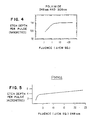
- the etch rate of polyimide at these wavelengths saturates at approximately 3-5 J/cm2. and remains relatively constant thereafter.
- a metal such as copper (of a few microns thickness) will be rapidly removed by laser pulses having energy fluences greater than this amount.
- This type of saturation may exist for longer wavelengths and for shorter wavelengths than those illustrated in FIG. 4. It is anticipated that polyimide will saturate at a higher fluence if the wavelength is increased beyond 308 nm, and will saturate at a smaller fluence for wavelengths less than 248 nm. For example, the saturation level for 351 nm laser pulses is higher than that for 308 nm radiation, but only slightly higher.
- Fig. 5 is a plot of etch depth per pulse versus energy fluence per pulse for ablative photodecomposition of polymethyl methyacrylate (PMMA), at 248 nm. This plot also shows a saturation effect in the etch rate of the polymer, where the saturation occurs in the approximate range of 4-8 J/cm2. This saturation effect is even more pronounced when the energy fluence for ablative photocomposition is approximately 24 J/cm2.
- the removal rate of a metal at these high fluences is extremely large, and several microns of metal can be removed in a single laser pulse at these fluence levels.
- a multilayer structure comprising polyimide and copper has been selectively etched to remove a copper layer without undue etching or harm to the polyimide layers.
- selective etching can be accomplished.
- Four micrometres of sputtered copper film on cured polyimide can be etched in about two laser pulses and a fluence of approximately 4J/cm2 at 248 nm and 351 nm.
- the polyimide removal rate at such fluences is very small, and is approximately 1 micron/pulse at 351 nm.
- a sputtered copper film of 4 micrometres thickness is etched in 1-2 pulses, while 7 pulses at the same energy fluence and wavelength are required to etch 5 micrometres of polyimide.
- the relative rates of etching of the copper and polyimide are very dissimilar and selective etching of a multilayer structure can be done without harm to surrounding or underlying metal layers.
- the reflectivity of many metals is substantially reduced in the wavelength range used in this invention.
- copper has a reflectivity in the visible and infrared regions which is greater than 90%.
- the reflectivity of copper drops to less than 50% in the wavelength range used in the present invention.
- This in combination with the high absorption coefficient of polymers at these wavelengths, leads to almost total absorption of the ultraviolet radiation in an extremely thin surface region of the polymer, thereby leaving the bulk of the polymer unetched and otherwise unharmed.
- a thin surface region of polyimide less than 1 micrometre thick would be affected by an ultraviolet pulse in this range of wavelengths, while several micrometres of copper would be totally removed by this single laser pulse.
- selected regions of a metal such as copper, Cu-doped Al, titanium, tungsten, etc. can be removed rapidly with one or two laser pulses, while the same laser pulses will affect only a very thin surface region of the polymer, if the wavelength and energy fluence per pulse of the ultraviolet radiation are suitably chosen. This choice is such that a considerable depth of metal is removed rapidly while the polymer is ablatively photodecomposed by only a minimum amount. Thermal effects are not necessarily a dominant mechanism in the ablation of the polymer, but are probably the dominant effect in the metal removal process.
- ablative photodecomposition of polymers will occur at low energy thresholds, approximating 10-30 mJ/cm2. However, at these energy fluence levels, no metal removal is observed. Thus, this is not an appropriate regime for a selective etching operation. Instead, the energy fluence per pulse has to be sufficiently high that the metal removal rate is rapid, while the polymer etch rate due to ablative photodecomposition is small (and preferably has levelled-off) with respect to the metal removal rate.
- Metals and polymers other than those specifically illustrated herein can be envisioned for specified wavelengths and energy fluences in order to provide selective removal of these metals from multilayer structures.
Landscapes
- Engineering & Computer Science (AREA)
- Physics & Mathematics (AREA)
- General Physics & Mathematics (AREA)
- Microelectronics & Electronic Packaging (AREA)
- Manufacturing & Machinery (AREA)
- Computer Hardware Design (AREA)
- Power Engineering (AREA)
- Condensed Matter Physics & Semiconductors (AREA)
- Optics & Photonics (AREA)
- High Energy & Nuclear Physics (AREA)
- Chemical & Material Sciences (AREA)
- Organic Chemistry (AREA)
- Mechanical Engineering (AREA)
- Electromagnetism (AREA)
- Plasma & Fusion (AREA)
- Health & Medical Sciences (AREA)
- Toxicology (AREA)
- Drying Of Semiconductors (AREA)
- Laser Beam Processing (AREA)
- ing And Chemical Polishing (AREA)
- Treatments Of Macromolecular Shaped Articles (AREA)
Applications Claiming Priority (2)
| Application Number | Priority Date | Filing Date | Title |
|---|---|---|---|
| US06/793,608 US4684437A (en) | 1985-10-31 | 1985-10-31 | Selective metal etching in metal/polymer structures |
| US793608 | 1985-10-31 |
Publications (3)
| Publication Number | Publication Date |
|---|---|
| EP0227903A2 EP0227903A2 (en) | 1987-07-08 |
| EP0227903A3 EP0227903A3 (en) | 1988-11-23 |
| EP0227903B1 true EP0227903B1 (en) | 1991-12-18 |
Family
ID=25160338
Family Applications (1)
| Application Number | Title | Priority Date | Filing Date |
|---|---|---|---|
| EP86114534A Expired - Lifetime EP0227903B1 (en) | 1985-10-31 | 1986-10-21 | A method of etching through a metal layer in a metal/polymer layered structure |
Country Status (4)
| Country | Link |
|---|---|
| US (1) | US4684437A (enExample) |
| EP (1) | EP0227903B1 (enExample) |
| JP (1) | JPS6336531A (enExample) |
| DE (1) | DE3683028D1 (enExample) |
Families Citing this family (102)
| Publication number | Priority date | Publication date | Assignee | Title |
|---|---|---|---|---|
| US4894598A (en) * | 1986-11-20 | 1990-01-16 | Staubli International Ag | Digital robot control having an improved pulse width modulator |
| US4882200A (en) * | 1987-05-21 | 1989-11-21 | General Electric Company | Method for photopatterning metallization via UV-laser ablation of the activator |
| US5269868A (en) * | 1989-10-12 | 1993-12-14 | Mitsubishi Denki Kabushiki Kaisha | Method for separating bonded substrates, in particular disassembling a liquid crystal display device |
| US5066357A (en) * | 1990-01-11 | 1991-11-19 | Hewlett-Packard Company | Method for making flexible circuit card with laser-contoured vias and machined capacitors |
| US5093279A (en) * | 1991-02-01 | 1992-03-03 | International Business Machines Corporation | Laser ablation damascene process |
| US5221426A (en) * | 1991-11-29 | 1993-06-22 | Motorola Inc. | Laser etch-back process for forming a metal feature on a non-metal substrate |
| CA2097388A1 (en) * | 1992-07-16 | 1994-01-17 | Susan Nord Bohlke | Topographical selective patterns |
| JP2951215B2 (ja) * | 1993-09-10 | 1999-09-20 | レイセオン・カンパニー | 位相マスクレーザによる微細なパターンの電子相互接続構造の製造方法 |
| US5841099A (en) * | 1994-07-18 | 1998-11-24 | Electro Scientific Industries, Inc. | Method employing UV laser pulses of varied energy density to form depthwise self-limiting blind vias in multilayered targets |
| US5843363A (en) * | 1995-03-31 | 1998-12-01 | Siemens Aktiengesellschaft | Ablation patterning of multi-layered structures |
| US6025256A (en) * | 1997-01-06 | 2000-02-15 | Electro Scientific Industries, Inc. | Laser based method and system for integrated circuit repair or reconfiguration |
| US6057180A (en) * | 1998-06-05 | 2000-05-02 | Electro Scientific Industries, Inc. | Method of severing electrically conductive links with ultraviolet laser output |
| US6207553B1 (en) | 1999-01-26 | 2001-03-27 | Advanced Micro Devices, Inc. | Method of forming multiple levels of patterned metallization |
| US6662439B1 (en) | 1999-10-04 | 2003-12-16 | Roche Diagnostics Corporation | Laser defined features for patterned laminates and electrodes |
| US7073246B2 (en) | 1999-10-04 | 2006-07-11 | Roche Diagnostics Operations, Inc. | Method of making a biosensor |
| US6645359B1 (en) | 2000-10-06 | 2003-11-11 | Roche Diagnostics Corporation | Biosensor |
| US6540890B1 (en) * | 2000-11-01 | 2003-04-01 | Roche Diagnostics Corporation | Biosensor |
| ES2675787T3 (es) | 2003-06-20 | 2018-07-12 | F. Hoffmann-La Roche Ag | Método y reactivo para producir tiras reactivas estrechas y homogéneas |
| JP2005118821A (ja) * | 2003-10-16 | 2005-05-12 | Olympus Corp | 超短パルスレーザ加工方法 |
| US20070232628A1 (en) * | 2004-05-06 | 2007-10-04 | Luengo Juan I | Calcilytic Compounds |
| JP4842927B2 (ja) * | 2004-05-10 | 2011-12-21 | パナソニック株式会社 | 超高速レーザパターニングに用いる複合シート材料選択方法 |
| GB0511132D0 (en) * | 2005-06-01 | 2005-07-06 | Plastic Logic Ltd | Layer-selective laser ablation patterning |
| EP1897157B1 (en) | 2005-06-01 | 2019-08-21 | Flexenable Limited | Layer-selective laser ablation patterning |
| TWI478351B (zh) * | 2006-07-20 | 2015-03-21 | Au Optronics Corp | 陣列基板之形成方法 |
| EP3142126A1 (en) * | 2008-03-06 | 2017-03-15 | Panduit Corp | Communication cable with improved crosstalk attenuation |
| US8183462B2 (en) * | 2008-05-19 | 2012-05-22 | Panduit Corp. | Communication cable with improved crosstalk attenuation |
| US8354590B2 (en) | 2008-11-10 | 2013-01-15 | Panduit Corp. | Communication cable with improved crosstalk attenuation |
| US8558115B2 (en) | 2009-03-03 | 2013-10-15 | Panduit Corp. | Communication cable including a mosaic tape |
| US8642448B2 (en) | 2010-06-22 | 2014-02-04 | Applied Materials, Inc. | Wafer dicing using femtosecond-based laser and plasma etch |
| US8507363B2 (en) | 2011-06-15 | 2013-08-13 | Applied Materials, Inc. | Laser and plasma etch wafer dicing using water-soluble die attach film |
| US20120322235A1 (en) * | 2011-06-15 | 2012-12-20 | Wei-Sheng Lei | Wafer dicing using hybrid galvanic laser scribing process with plasma etch |
| US9029242B2 (en) | 2011-06-15 | 2015-05-12 | Applied Materials, Inc. | Damage isolation by shaped beam delivery in laser scribing process |
| US8557683B2 (en) | 2011-06-15 | 2013-10-15 | Applied Materials, Inc. | Multi-step and asymmetrically shaped laser beam scribing |
| US8759197B2 (en) | 2011-06-15 | 2014-06-24 | Applied Materials, Inc. | Multi-step and asymmetrically shaped laser beam scribing |
| US9129904B2 (en) | 2011-06-15 | 2015-09-08 | Applied Materials, Inc. | Wafer dicing using pulse train laser with multiple-pulse bursts and plasma etch |
| US8598016B2 (en) * | 2011-06-15 | 2013-12-03 | Applied Materials, Inc. | In-situ deposited mask layer for device singulation by laser scribing and plasma etch |
| US8703581B2 (en) | 2011-06-15 | 2014-04-22 | Applied Materials, Inc. | Water soluble mask for substrate dicing by laser and plasma etch |
| US8912077B2 (en) | 2011-06-15 | 2014-12-16 | Applied Materials, Inc. | Hybrid laser and plasma etch wafer dicing using substrate carrier |
| US8501613B2 (en) * | 2011-07-07 | 2013-08-06 | Taiwan Semiconductor Manufacturing Company, Ltd. | UBM etching methods for eliminating undercut |
| US8946057B2 (en) | 2012-04-24 | 2015-02-03 | Applied Materials, Inc. | Laser and plasma etch wafer dicing using UV-curable adhesive film |
| US9048309B2 (en) | 2012-07-10 | 2015-06-02 | Applied Materials, Inc. | Uniform masking for wafer dicing using laser and plasma etch |
| US8859397B2 (en) | 2012-07-13 | 2014-10-14 | Applied Materials, Inc. | Method of coating water soluble mask for laser scribing and plasma etch |
| US8940619B2 (en) | 2012-07-13 | 2015-01-27 | Applied Materials, Inc. | Method of diced wafer transportation |
| US9252057B2 (en) | 2012-10-17 | 2016-02-02 | Applied Materials, Inc. | Laser and plasma etch wafer dicing with partial pre-curing of UV release dicing tape for film frame wafer application |
| US8975162B2 (en) | 2012-12-20 | 2015-03-10 | Applied Materials, Inc. | Wafer dicing from wafer backside |
| US9236305B2 (en) | 2013-01-25 | 2016-01-12 | Applied Materials, Inc. | Wafer dicing with etch chamber shield ring for film frame wafer applications |
| TWI619165B (zh) | 2013-03-14 | 2018-03-21 | 應用材料股份有限公司 | 以雷射及電漿蝕刻進行的基板切割所用的含非光可界定雷射能量吸收層的多層遮罩 |
| US9105710B2 (en) | 2013-08-30 | 2015-08-11 | Applied Materials, Inc. | Wafer dicing method for improving die packaging quality |
| US9224650B2 (en) | 2013-09-19 | 2015-12-29 | Applied Materials, Inc. | Wafer dicing from wafer backside and front side |
| US9460966B2 (en) | 2013-10-10 | 2016-10-04 | Applied Materials, Inc. | Method and apparatus for dicing wafers having thick passivation polymer layer |
| US9041198B2 (en) | 2013-10-22 | 2015-05-26 | Applied Materials, Inc. | Maskless hybrid laser scribing and plasma etching wafer dicing process |
| US9312177B2 (en) | 2013-12-06 | 2016-04-12 | Applied Materials, Inc. | Screen print mask for laser scribe and plasma etch wafer dicing process |
| US9299614B2 (en) | 2013-12-10 | 2016-03-29 | Applied Materials, Inc. | Method and carrier for dicing a wafer |
| US10109612B2 (en) * | 2013-12-13 | 2018-10-23 | Taiwan Semiconductor Manufacturing Company | Tools and systems for processing semiconductor devices, and methods of processing semiconductor devices |
| US9293304B2 (en) | 2013-12-17 | 2016-03-22 | Applied Materials, Inc. | Plasma thermal shield for heat dissipation in plasma chamber |
| US9018079B1 (en) | 2014-01-29 | 2015-04-28 | Applied Materials, Inc. | Wafer dicing using hybrid laser scribing and plasma etch approach with intermediate reactive post mask-opening clean |
| US9299611B2 (en) | 2014-01-29 | 2016-03-29 | Applied Materials, Inc. | Method of wafer dicing using hybrid laser scribing and plasma etch approach with mask plasma treatment for improved mask etch resistance |
| US8991329B1 (en) | 2014-01-31 | 2015-03-31 | Applied Materials, Inc. | Wafer coating |
| US9236284B2 (en) | 2014-01-31 | 2016-01-12 | Applied Materials, Inc. | Cooled tape frame lift and low contact shadow ring for plasma heat isolation |
| US9275902B2 (en) | 2014-03-26 | 2016-03-01 | Applied Materials, Inc. | Dicing processes for thin wafers with bumps on wafer backside |
| US9076860B1 (en) | 2014-04-04 | 2015-07-07 | Applied Materials, Inc. | Residue removal from singulated die sidewall |
| US8975163B1 (en) | 2014-04-10 | 2015-03-10 | Applied Materials, Inc. | Laser-dominated laser scribing and plasma etch hybrid wafer dicing |
| US8932939B1 (en) | 2014-04-14 | 2015-01-13 | Applied Materials, Inc. | Water soluble mask formation by dry film lamination |
| US8912078B1 (en) | 2014-04-16 | 2014-12-16 | Applied Materials, Inc. | Dicing wafers having solder bumps on wafer backside |
| US8999816B1 (en) | 2014-04-18 | 2015-04-07 | Applied Materials, Inc. | Pre-patterned dry laminate mask for wafer dicing processes |
| US8912075B1 (en) | 2014-04-29 | 2014-12-16 | Applied Materials, Inc. | Wafer edge warp supression for thin wafer supported by tape frame |
| US9159621B1 (en) | 2014-04-29 | 2015-10-13 | Applied Materials, Inc. | Dicing tape protection for wafer dicing using laser scribe process |
| US8980727B1 (en) | 2014-05-07 | 2015-03-17 | Applied Materials, Inc. | Substrate patterning using hybrid laser scribing and plasma etching processing schemes |
| US9112050B1 (en) | 2014-05-13 | 2015-08-18 | Applied Materials, Inc. | Dicing tape thermal management by wafer frame support ring cooling during plasma dicing |
| US9034771B1 (en) | 2014-05-23 | 2015-05-19 | Applied Materials, Inc. | Cooling pedestal for dicing tape thermal management during plasma dicing |
| US9754823B2 (en) | 2014-05-28 | 2017-09-05 | International Business Machines Corporation | Substrate including selectively formed barrier layer |
| US9165832B1 (en) | 2014-06-30 | 2015-10-20 | Applied Materials, Inc. | Method of die singulation using laser ablation and induction of internal defects with a laser |
| US9142459B1 (en) | 2014-06-30 | 2015-09-22 | Applied Materials, Inc. | Wafer dicing using hybrid laser scribing and plasma etch approach with mask application by vacuum lamination |
| US9130057B1 (en) | 2014-06-30 | 2015-09-08 | Applied Materials, Inc. | Hybrid dicing process using a blade and laser |
| US9093518B1 (en) | 2014-06-30 | 2015-07-28 | Applied Materials, Inc. | Singulation of wafers having wafer-level underfill |
| US9349648B2 (en) | 2014-07-22 | 2016-05-24 | Applied Materials, Inc. | Hybrid wafer dicing approach using a rectangular shaped two-dimensional top hat laser beam profile or a linear shaped one-dimensional top hat laser beam profile laser scribing process and plasma etch process |
| US9196498B1 (en) | 2014-08-12 | 2015-11-24 | Applied Materials, Inc. | Stationary actively-cooled shadow ring for heat dissipation in plasma chamber |
| US9117868B1 (en) | 2014-08-12 | 2015-08-25 | Applied Materials, Inc. | Bipolar electrostatic chuck for dicing tape thermal management during plasma dicing |
| US9281244B1 (en) | 2014-09-18 | 2016-03-08 | Applied Materials, Inc. | Hybrid wafer dicing approach using an adaptive optics-controlled laser scribing process and plasma etch process |
| US9177861B1 (en) | 2014-09-19 | 2015-11-03 | Applied Materials, Inc. | Hybrid wafer dicing approach using laser scribing process based on an elliptical laser beam profile or a spatio-temporal controlled laser beam profile |
| US11195756B2 (en) | 2014-09-19 | 2021-12-07 | Applied Materials, Inc. | Proximity contact cover ring for plasma dicing |
| US9196536B1 (en) | 2014-09-25 | 2015-11-24 | Applied Materials, Inc. | Hybrid wafer dicing approach using a phase modulated laser beam profile laser scribing process and plasma etch process |
| US9130056B1 (en) | 2014-10-03 | 2015-09-08 | Applied Materials, Inc. | Bi-layer wafer-level underfill mask for wafer dicing and approaches for performing wafer dicing |
| US9245803B1 (en) | 2014-10-17 | 2016-01-26 | Applied Materials, Inc. | Hybrid wafer dicing approach using a bessel beam shaper laser scribing process and plasma etch process |
| US10692765B2 (en) | 2014-11-07 | 2020-06-23 | Applied Materials, Inc. | Transfer arm for film frame substrate handling during plasma singulation of wafers |
| US9159624B1 (en) | 2015-01-05 | 2015-10-13 | Applied Materials, Inc. | Vacuum lamination of polymeric dry films for wafer dicing using hybrid laser scribing and plasma etch approach |
| US9330977B1 (en) | 2015-01-05 | 2016-05-03 | Applied Materials, Inc. | Hybrid wafer dicing approach using a galvo scanner and linear stage hybrid motion laser scribing process and plasma etch process |
| US9355907B1 (en) | 2015-01-05 | 2016-05-31 | Applied Materials, Inc. | Hybrid wafer dicing approach using a line shaped laser beam profile laser scribing process and plasma etch process |
| US9601375B2 (en) | 2015-04-27 | 2017-03-21 | Applied Materials, Inc. | UV-cure pre-treatment of carrier film for wafer dicing using hybrid laser scribing and plasma etch approach |
| US9478455B1 (en) | 2015-06-12 | 2016-10-25 | Applied Materials, Inc. | Thermal pyrolytic graphite shadow ring assembly for heat dissipation in plasma chamber |
| US9721839B2 (en) | 2015-06-12 | 2017-08-01 | Applied Materials, Inc. | Etch-resistant water soluble mask for hybrid wafer dicing using laser scribing and plasma etch |
| US9972575B2 (en) | 2016-03-03 | 2018-05-15 | Applied Materials, Inc. | Hybrid wafer dicing approach using a split beam laser scribing process and plasma etch process |
| US9852997B2 (en) | 2016-03-25 | 2017-12-26 | Applied Materials, Inc. | Hybrid wafer dicing approach using a rotating beam laser scribing process and plasma etch process |
| US9793132B1 (en) | 2016-05-13 | 2017-10-17 | Applied Materials, Inc. | Etch mask for hybrid laser scribing and plasma etch wafer singulation process |
| US11158540B2 (en) | 2017-05-26 | 2021-10-26 | Applied Materials, Inc. | Light-absorbing mask for hybrid laser scribing and plasma etch wafer singulation process |
| US10363629B2 (en) | 2017-06-01 | 2019-07-30 | Applied Materials, Inc. | Mitigation of particle contamination for wafer dicing processes |
| US10535561B2 (en) | 2018-03-12 | 2020-01-14 | Applied Materials, Inc. | Hybrid wafer dicing approach using a multiple pass laser scribing process and plasma etch process |
| US11355394B2 (en) | 2018-09-13 | 2022-06-07 | Applied Materials, Inc. | Wafer dicing using hybrid laser scribing and plasma etch approach with intermediate breakthrough treatment |
| US11011424B2 (en) | 2019-08-06 | 2021-05-18 | Applied Materials, Inc. | Hybrid wafer dicing approach using a spatially multi-focused laser beam laser scribing process and plasma etch process |
| US11342226B2 (en) | 2019-08-13 | 2022-05-24 | Applied Materials, Inc. | Hybrid wafer dicing approach using an actively-focused laser beam laser scribing process and plasma etch process |
| US10903121B1 (en) | 2019-08-14 | 2021-01-26 | Applied Materials, Inc. | Hybrid wafer dicing approach using a uniform rotating beam laser scribing process and plasma etch process |
| US11600492B2 (en) | 2019-12-10 | 2023-03-07 | Applied Materials, Inc. | Electrostatic chuck with reduced current leakage for hybrid laser scribing and plasma etch wafer singulation process |
Family Cites Families (3)
| Publication number | Priority date | Publication date | Assignee | Title |
|---|---|---|---|---|
| US4568632A (en) * | 1982-10-07 | 1986-02-04 | International Business Machines Corporation | Patterning of polyimide films with far ultraviolet light |
| US4414059A (en) * | 1982-12-09 | 1983-11-08 | International Business Machines Corporation | Far UV patterning of resist materials |
| US4490211A (en) * | 1984-01-24 | 1984-12-25 | International Business Machines Corporation | Laser induced chemical etching of metals with excimer lasers |
-
1985
- 1985-10-31 US US06/793,608 patent/US4684437A/en not_active Expired - Lifetime
-
1986
- 1986-07-29 JP JP61176870A patent/JPS6336531A/ja active Granted
- 1986-10-21 EP EP86114534A patent/EP0227903B1/en not_active Expired - Lifetime
- 1986-10-21 DE DE8686114534T patent/DE3683028D1/de not_active Expired - Lifetime
Also Published As
| Publication number | Publication date |
|---|---|
| JPS6336531A (ja) | 1988-02-17 |
| DE3683028D1 (de) | 1992-01-30 |
| EP0227903A3 (en) | 1988-11-23 |
| EP0227903A2 (en) | 1987-07-08 |
| JPH0528897B2 (enExample) | 1993-04-27 |
| US4684437A (en) | 1987-08-04 |
Similar Documents
| Publication | Publication Date | Title |
|---|---|---|
| EP0227903B1 (en) | A method of etching through a metal layer in a metal/polymer layered structure | |
| US5505320A (en) | Method employing laser ablating for providing a pattern on a substrate | |
| US5302547A (en) | Systems for patterning dielectrics by laser ablation | |
| US5236551A (en) | Rework of polymeric dielectric electrical interconnect by laser photoablation | |
| CN101448603B (zh) | 提高激光通孔钻凿产量和清洁表面的方法及其系统 | |
| JP4788712B2 (ja) | 制御された熱的、物理的改質を用いるパルスレーザ処理。 | |
| KR100258287B1 (ko) | 다층 타겟에 경유로를 형성하는 방법과 자외선 레이저 시스템(Ultraviolet laser system and method for forming vias in multi-layered targets) | |
| US20050115937A1 (en) | Laser-based method and system for memory link processing with picosecond lasers | |
| JPH08274064A (ja) | 多層工作物をパターン加工する方法 | |
| JP2002535701A (ja) | 薄膜にパターンを形成する方法 | |
| US4898648A (en) | Method for providing a strengthened conductive circuit pattern | |
| US5332879A (en) | Method for removing trace metal contaminants from organic dielectrics | |
| JP2584884B2 (ja) | 配線基板 | |
| CN101175598A (zh) | 用于双头激光微加工系统的合成脉冲重复率处理 | |
| EP0108189B1 (en) | A method for etching polyimides | |
| US4909895A (en) | System and method for providing a conductive circuit pattern utilizing thermal oxidation | |
| JP2002164591A (ja) | 半導体装置およびその半導体装置の製造方法 | |
| Metev et al. | Pattern generation by laser-induced oxidation of thin metal films (microcircuit fabrication) | |
| Elliott et al. | Single & Multiple Pulse Ablation of Polymeric and High Density Materials with Excimer Laser Radiation at 193NM and 248NM | |
| Ashkenasi et al. | Processing multilayer systems using femtosecond, picosecond, and nanosecond laser pulses at different wavelengths | |
| JP3052226B2 (ja) | レーザ加工法および加工装置 | |
| JP2002331378A (ja) | レーザ加工方法 | |
| JP3343812B2 (ja) | バイアホール形成方法及びレーザ加工装置 | |
| Poulin et al. | Advances in excimer laser materials processing | |
| Okoshi et al. | Microfabrication of polyethylene using femtosecond Ti: sapphire laser and nanosecond ArF laser |
Legal Events
| Date | Code | Title | Description |
|---|---|---|---|
| PUAI | Public reference made under article 153(3) epc to a published international application that has entered the european phase |
Free format text: ORIGINAL CODE: 0009012 |
|
| AK | Designated contracting states |
Kind code of ref document: A2 Designated state(s): DE FR GB IT |
|
| 17P | Request for examination filed |
Effective date: 19870821 |
|
| PUAL | Search report despatched |
Free format text: ORIGINAL CODE: 0009013 |
|
| AK | Designated contracting states |
Kind code of ref document: A3 Designated state(s): DE FR GB IT |
|
| 17Q | First examination report despatched |
Effective date: 19900731 |
|
| GRAA | (expected) grant |
Free format text: ORIGINAL CODE: 0009210 |
|
| AK | Designated contracting states |
Kind code of ref document: B1 Designated state(s): DE FR GB IT |
|
| PG25 | Lapsed in a contracting state [announced via postgrant information from national office to epo] |
Ref country code: IT Free format text: LAPSE BECAUSE OF FAILURE TO SUBMIT A TRANSLATION OF THE DESCRIPTION OR TO PAY THE FEE WITHIN THE PRESCRIBED TIME-LIMIT;WARNING: LAPSES OF ITALIAN PATENTS WITH EFFECTIVE DATE BEFORE 2007 MAY HAVE OCCURRED AT ANY TIME BEFORE 2007. THE CORRECT EFFECTIVE DATE MAY BE DIFFERENT FROM THE ONE RECORDED. Effective date: 19911218 |
|
| ET | Fr: translation filed | ||
| REF | Corresponds to: |
Ref document number: 3683028 Country of ref document: DE Date of ref document: 19920130 |
|
| PLBE | No opposition filed within time limit |
Free format text: ORIGINAL CODE: 0009261 |
|
| STAA | Information on the status of an ep patent application or granted ep patent |
Free format text: STATUS: NO OPPOSITION FILED WITHIN TIME LIMIT |
|
| 26N | No opposition filed | ||
| PGFP | Annual fee paid to national office [announced via postgrant information from national office to epo] |
Ref country code: DE Payment date: 19951030 Year of fee payment: 10 |
|
| PGFP | Annual fee paid to national office [announced via postgrant information from national office to epo] |
Ref country code: GB Payment date: 19960925 Year of fee payment: 11 |
|
| PGFP | Annual fee paid to national office [announced via postgrant information from national office to epo] |
Ref country code: FR Payment date: 19961007 Year of fee payment: 11 |
|
| PG25 | Lapsed in a contracting state [announced via postgrant information from national office to epo] |
Ref country code: DE Effective date: 19970701 |
|
| PG25 | Lapsed in a contracting state [announced via postgrant information from national office to epo] |
Ref country code: GB Free format text: LAPSE BECAUSE OF NON-PAYMENT OF DUE FEES Effective date: 19971021 |
|
| PG25 | Lapsed in a contracting state [announced via postgrant information from national office to epo] |
Ref country code: FR Free format text: THE PATENT HAS BEEN ANNULLED BY A DECISION OF A NATIONAL AUTHORITY Effective date: 19971031 |
|
| GBPC | Gb: european patent ceased through non-payment of renewal fee |
Effective date: 19971021 |
|
| REG | Reference to a national code |
Ref country code: FR Ref legal event code: ST |