EP0226950B1 - Memory access control circuit - Google Patents
Memory access control circuit Download PDFInfo
- Publication number
- EP0226950B1 EP0226950B1 EP86117189A EP86117189A EP0226950B1 EP 0226950 B1 EP0226950 B1 EP 0226950B1 EP 86117189 A EP86117189 A EP 86117189A EP 86117189 A EP86117189 A EP 86117189A EP 0226950 B1 EP0226950 B1 EP 0226950B1
- Authority
- EP
- European Patent Office
- Prior art keywords
- address
- signal
- memory
- data
- output
- Prior art date
- Legal status (The legal status is an assumption and is not a legal conclusion. Google has not performed a legal analysis and makes no representation as to the accuracy of the status listed.)
- Expired - Lifetime
Links
Images


Classifications
-
- G—PHYSICS
- G06—COMPUTING OR CALCULATING; COUNTING
- G06F—ELECTRIC DIGITAL DATA PROCESSING
- G06F12/00—Accessing, addressing or allocating within memory systems or architectures
- G06F12/02—Addressing or allocation; Relocation
- G06F12/0215—Addressing or allocation; Relocation with look ahead addressing means
Definitions
- the present invention relates to a memory access control circuit for controlling dynamic RAM access and, more particularly, to a memory access control circuit for efficiently accessing a dynamic RAM having a page or static column mode.
- An address is input to a dynamic RAM (to be referred to as a DRAM hereinafter) such that address data is divided into upper and lower address signals and these signals are time-divisionally multiplexed.
- the access time in the DRAM data read mode is defined by a period required for identifying data after the upper and lower address signals are input to the DRAM. Since each address data is divided into two address signals and these signals are input to the DRAM, the access time is undesirably prolonged.
- a CPU or DMA controller tends to access data having successive or adjacent addresses. In this case, data having the same upper address but different lower addresses is frequently accessed.
- second lower address (01) H is input to the DRAM.
- signal CAS goes to level "0". Since all the data corresponding to address (01) H in the DRAM has been accessed, only the data corresponding to this lower address is selected from the accessed data and output outside the DRAM. Therefore, data B stored at address (0101)H of the DRAM is read out. Similarly, data is sequentially selected and output in response to the lower address inputs and falling of signal CAS to level "0" in synchronism with each lower address input.
- Static column access employs the same addressing as that of page mode access.
- signal CAS is set to be continuously active (level "0") within the period for inputting a plurality of lower addresses. Since the logical level of signal CAS need not be repeatedly changed, data access can be achieved at a higher speed.
- page mode access and static column access are based on the assumption that the upper address is not frequently updated. In other words, if the upper address is frequently updated, high-speed access cannot be performed.
- a conventional device e.g., a CPU or a DMA controller
- a function for discriminating whether or not the upper address is updated does not have a function for discriminating whether or not the upper address is updated.
- the conventional CPU or DMA controller cannot employ a page mode access or static column access function assigned to the DRAM.
- PANAFACOM Prior art document EP-A-0 025 801 discloses a circuit arrangement that effectively discriminates whether or not the upper portion of the address is updated, but does not actually employ page mode memory access, so that at every memory cycle lower and upper portions of the address are sequentially supplied to the DRAM.
- a memory access control circuit comprising a memory access circuit for output-ting memory address data consisting of upper and lower address signals to access a memory and for requesting updating of a memory address as needed, address retaining means for retaining the upper and lower address signals output from the memory access circuit and for updating the memory address by a predetermined value on the basis of a control signal, upper address detecting means for detecting a change in upper address signal output from the memory access circuit, address switching means for sequentially switching and outputting the upper and lower address signals retained by the address retaining means, an address bus to which multiplexed upper and lower address signals output from the address switching means are transferred, a memory for receiving the multiplexed upper and lower address signals from the address bus, and control means for controlling the address switching means, to send only the lower address signal onto the address bus when an output from the upper address detecting means represents no updating of the upper address signal, and to send the sequentially switched upper and lower address signals onto the address bus when the output from the upper address detecting
- Fig. 3 is a block diagram showing a memory access control circuit according to an embodiment of the present invention.
- reference numeral 11 denotes a memory access circuit (e.g., a CPU or a DMA controller) having a memory access function.
- Access circuit 11 generates upper address signal UA, Lower address signal LA, address strobe signal AS, and count-up control signal CU in order to access a memory.
- Upper and lower address signals UA and LA, address strobe signal AS and count-up control signal CU are supplied from memory access circuit 11 to address counter 12.
- Counter 12 comprises upper and lower address counters 12U and 12L for retaining the upper and lower address signals. In practice, counter 12 retains address signals UA and LA in response to strobe signal AS. When counter 12 receives signal CU, the retained value is updated by a predetermined value, e.g., incremented by one.
- Signals UA and LA retained in counter 12 are output as upper and lower memory address signals UMA and LMA, respectively.
- Upper and lower memory address signals UMA and LMA are supplied from address counter 12 to multiplexer 13.
- Multiplexer 13 time-divisionally sends address signals UMA and LMA onto address bus 14 in response to address switching signal ASE (to be described later).
- Upper memory address signal LMA output from address counter 12 is input to old address register 15.
- register 15 Upon reception of new address signal NA (to be described later), register 15 stores it as upper memory address signal UMA and outputs it as old address signal OMA.
- Old address signal OMA and upper memory address UMA are input to address comparator 16.
- Comparator 16 compares signal OMA with signal UMA and determines a coincidence therebetween. If a noncoincidence is established, comparator 16 generates noncoincidence signal NE. Signal NE is input to timing control circuit 17.
- Timing control circuit 17 also receives address strobe signal AS, count-up control signal CU, and reset signal RST. Control circuit 17 outputs address switching signal ASE, new address signal NA, row address strobe signal RSA , column address strobe signal CAS , and wait signal WAI on the basis of the above input signals. Signal WAI is input to memory access circuit 11. Signals RAS and CAS are input to DRAM 18.
- DRAM 18 is connected to address bus 14.
- DRAM 18 and memory access circuit 11 are connected via data bus 19.
- the timing chart in Fig. 4 shows the sequence wherein memory access circuit 11 sequentially accesses three addresses (0100) H , (0101) H , and (0201) H after reset signal RST is input to timing control circuit 17.
- first data for address (0100) H is output from memory access circuit 11.
- address strobe signal AS goes to level "1".
- the address output from access circuit 11 is divided into upper and lower address signals UA and LA.
- Signal UA has an address value of (01) H
- signal LA has an address value of (00) H .
- address counter 12 retains these signals UA and LA.
- the address data is not retained in old address register 15, and its value is indefinite. For this reason, the result of comparison between signals UMA and OMA by address comparator 16 results in a noncoincidence, so that comparator 16 outputs noncoincidence signal NE.
- control circuit 17 outputs new address signal NA.
- register 15 stores and retains address signal UMA having a value of (01) H .
- address switching signal ASE is set to be level "1" by timing control circuit 17.
- signal ASE goes to level "1"
- multiplexer 13 switches to upper memory address (01) H received from address counter 12 during this period and outputs it onto address bus 14.
- signal ASE is set at level "0" in timing control circuit 17.
- multiplexer 13 switches to lower memory address (00) H received from address counter 12 and outputs it onto address bus 14.
- second data for address (0101) H is output from memory access circuit 11, and address strobe signal AS is output in response thereto.
- the address data is divided into upper and lower address signals UA and LA in the same manner as described above.
- address register 15 retains signal UMA for previous upper memory address signal (01) H .
- This address signal UMA coincides with old address signal OMA, and address comparator 16 does not output noncoincidence signal NE.
- timing control circuit 17 does not output new address signal NA.
- the retained value of register 15 is kept unchanged.
- address switching signal ASE is kept at level "0", and only signal CAS goes to level "0"
- Multiplexer 13 then switches to lower memory address (01) H received from counter 12 and outputs it onto address bus 14.
- DRAM 18 On the basis of signal CAS , DRAM 18 receives signal LA for lower memory address (01) H . Thereafter, data is read out from DRAM 18 by a combination of signals UA and LA, respectively, for upper and lower memory addresses (01) H and (01) H . The readout data is transferred to memory access circuit 11 via data bus 19.
- DRAM 18 is accessed by outputting only lower memory address signal LMA onto address bus 14 when upper address signal UA is not updated.
- Third data for address (0201) H is output from memory access circuit 11.
- signal UA for upper address (02) H and signal LA for lower address (01) H are sent to address counter 12.
- Old address register 15 retains signal UMA for previous upper memory address (01) H .
- No coincidence is established between signal UMA and old address OMA, and address comparator 16 outputs noncoincidence signal NE.
- timing control circuit 17 Upon reception of signal NE, timing control circuit 17 outputs new address signal NA.
- Old address register 15 receives signal UMA for upper memory address and old address signal OMA is updated. Thereafter, control circuit 17 sets signal RAS to level "1", signifying that page mode access of DRAM 18 has been completed.
- address switching signal ASE is set at level "1", and then signal RAS goes to level “0" again, thus signifying that new page mode access of DRAM 18 has started. While signal ASE is set at level "1", multiplexer 13 switches to signal UMA for upper memory address (02) H and outputs it onto address bus 14. DRAM 18 receives signal UMA in response to signal RAS . Subsequently, in timing control circuit 17, address switching signal ASE goes to level "0". For the period of this logic level, multiplexer 13 switches to signal UMA for lower memory address (01) H received from counter 12 and outputs it onto address bus 14. Thereafter, in control circuit 17, signal CAS goes to level "0".
- DRAM 18 receives signal LMA for lower memory address (01) H in response to signal CAS .
- Data is read out from DRAM 18 by a combination of signals UA and LA, respectively, for upper and lower addresses (02) H and (01) H .
- the readout data is transferred to memory access circuit 11 via data bus 19.
- Timing control circuit 17 outputs wait signal WAI when multiplexer 13 supplies upper memory address signal UMA onto address bus 14, signalling to memory access circuit 11 that the access time of DRAM 18 is prolonged.
- signal WAI is input to memory access circuit 11, circuit 11 prolongs current upper and lower address signals UA and LA so as to compensate for the access time of DRAM 18.
- the timing chart in Fig. 5 explains the operation wherein memory access circuit 11 sequentially accesses successive addresses from (00FE) H .
- Memory access circuit 11 outputs first data for address (00FE) H and address strobe signal AS. This output operation is the same as that in the timing chart of Fig. 4, and a detailed description thereof will be omitted.
- count-up control signal CU is output from memory access circuit 11.
- the prestored address signal value is incremented by one in address counter 12.
- Signal LMA retained and output from counter 12 is updated from lower memory address (FE) H to lower memory address (FF) H .
- signal UM for upper memory address (00) H is not changed.
- Address comparator 16 does not output noncoincidence signal NE. For this reason, the same access as that using only lower memory address signal LMA (Fig. 4) is performed.
- memory access circuit 11 In order to access the next address (0100) H , memory access circuit 11 outputs count-up control signal CU.
- Address counter 12 increments lower address signal LA value by one, so that address (FF) H is updated to (00) H .
- a carry from the lower address causes updating of upper address (00) H to (01) H .
- address comparator 16 Since the value of upper memory address signal UMA is changed, address comparator 16 outputs noncoincidence signal NE.
- the access operation is performed in the same manner as the case wherein higher memory address signal UAM is changed in the timing chart of Fig. 4. More specifically, new upper memory address signal UMA and lower memory address LMA are time-divisionally output to address bus 14, and thus DRAM 18 is accessed.
- memory access circuit 11 outputs count-up control signal CU. If address signal UMA is not changed upon incrementation of the retained value of address counter 12, only address signal LMA is used to access DRAM 18. However, if address signal UMA is changed, both new signal UMA and signal LMA are used to access DRAM 18.
- upper memory address signal UMA is supplied to DRAM 18 only when upper memory address signal UMA is changed. Otherwise, only lower memory address signal LMA is supplied to DRAM 18, thereby performing page mode access and hence achieving high-speed access of DRAM 18.
- Static column access for high-speed access of DRAM 18 is different from page mode access in the manner of generating column address strobe control signal CAS . If updating of the memory address signal output from memory access circuit 11 can be detected, DRAM 18 can be accessed according to static column access.
- state A various signals NA, ASE, WAI, RAS , and CAS are respectively set to be 0, 0, 0, 1, and 1.
- state B signals NA, ASE, WAI, RAS , and CAS are respectively set to be 1, 1, 1, 1 ⁇ 0, and 1. State B is unconditionally transited to state C.
- state C signals NA, ASE, WAI, RAS , and CAS are respectively set to be 0, 0, 0, 0, and 1 ⁇ 0 ⁇ 1.
- State C is unconditionally transited to state D.
- signals NA, ASE, WAI, RAS , and CAS are respectively set to be 0, 0, 0, 0, and 1.
- state E signals NA, ASE, WAI, RAS , and CAS are respectively set to be 1, 1, 1, 0 ⁇ 1 ⁇ 0, and 1.
- State E is unconditionally transited to state C. Control of timing control circuit 17 is performed according to page mode access.
- Fig. 7 is a state tradition diagram of timing control circuit 17 so as to control static column mode access.
- state A if reset signal RST is input, state A is initialized.
- signals NA, ASE, WAI, RAS , and CAS are respectively set to be 0, 0, 0, 1, and 1.
- state A if signal AS is set at level "0", state A continues. However, if signal AS goes to level "L”, state A is transited to state B.
- signals NA, ASE, WAI, RAS , and CAS are respectively set to be 1, 1, 1, 1 ⁇ 0, and 1.
- State B is unconditionally transited to state C.
- state C signals NA, ASE, WAI, RAS , and CAS are respectively set to be 0, 0, 0, 0, and 0.
- State C is unconditionally shifted to state D.
- state D signals NA, ASE, WAI, RAS , and CAS are respectively set to be 0, 0, 0, 0, and 0.
- signals NA, ASE, WAI, RAS , and CAS are respectively set to be 1, 1, 1, 0 ⁇ 1 ⁇ 0, and 0 ⁇ 1.
- State E is unconditionally transited to state C.
- signals NA, ASE, WAI, RAS , and CAS are respectively set to be 0, 0, 0, 0, and 0.
- State F is unconditionally transited to state D. In this manner, control of timing control circuit 17 is performed according to static column mode access.
- Fig. 8 is a block diagram of a memory access control circuit according to another embodiment of the present invention.
- Fig. 8 The embodiment in Fig. 8 is different from that in Fig. 3 in the following points.
- Address counter 22 capable of outputting outside the circuit carry output signal CO upon updating of the lower address signal is arranged in place of address counter 12. Old address register 15 and address comparator 16 are omitted, and instead OR gate 23 is arranged to receive address strobe signal AS and carry signal CO from counter 22. Noncoincidence signal NE2 from OR gate 23 is input to timing control circuit 27 used in place of timing control circuit 17.
- Control circuit 27 receives address strobe signal AS, count-up control signal CU, and reset signal RST in addition to signal NE2. On the basis of these input signals, control circuit 27 generates address switching signal ASE, row address strobe signal RAS , column address strobe signal CAS , and wait signal WAI.
- Counter 22 comprises upper and lower address counters 22U and 22L.
- First data of address (00FE) H from memory access circuit 11 is divided into upper and lower address signals UA and LA, and signals UMA and LMA are output therefrom.
- access circuit 11 outputs address strobe signal AS.
- Signal AS is input to OR gate 23 so that gate 23 then outputs noncoincidence signal NE2.
- OR gate 23 outputs signal NE2.
- Multiplexer 13 switches upper and lower address signals UMA and LMA for every signal NE2 so that address signals selectively appear on address bus 14.
- DRAM 18 receives address data on the basis of signals RAS and CAS output from timing control circuit 27. Data access is performed in response to such addressing.
- circuit 11 If memory access circuit 11 accesses second data for address (00FF) H next to address (00FE) H , circuit 11 outputs only count-up control signal CU. Upon reception of signal CU, only the value of lower address signal LA is incremented by one in address counter 22 so that the lower address is updated from (FE) H to (FF) H . In this case, no carry signal CO is generated by lower address counter 22L, and noncoincidence signal NE2 is not output from OR gate 23. In the same manner as in the case wherein upper memory address signal UMA is not changed in the timing chart of Fig. 4, DRAM 18 is accessed by only lower memory address signal LMA.
- the upper address signal is supplied to a memory (e.g., a DRAM) using a multiplexed address signal only when the upper address is updated.
- a memory e.g., a DRAM
- the upper address signal is not output when the upper address is not updated. Therefore, page mode access or static column access for shortening access time can be performed. Furthermore, since retaining and incrementing means of the memory address are arranged, page mode access or static column access can be performed such that only the start address is specified to access succeeding addresses and thereafter count-up control signal CU, is output from memory access circuit 11.
- counter 12 has its count incremented by one every time it receives signal CU from memory access circuit 11. Instead, counter can be replaced by a incremented by any other value every time it receives signal CU, said value being determined by another signal from memory access circuit 11.
Landscapes
- Engineering & Computer Science (AREA)
- Theoretical Computer Science (AREA)
- Physics & Mathematics (AREA)
- General Engineering & Computer Science (AREA)
- General Physics & Mathematics (AREA)
- Dram (AREA)
- Memory System (AREA)
Description
- The present invention relates to a memory access control circuit for controlling dynamic RAM access and, more particularly, to a memory access control circuit for efficiently accessing a dynamic RAM having a page or static column mode.
- An address is input to a dynamic RAM (to be referred to as a DRAM hereinafter) such that address data is divided into upper and lower address signals and these signals are time-divisionally multiplexed. The access time in the DRAM data read mode is defined by a period required for identifying data after the upper and lower address signals are input to the DRAM. Since each address data is divided into two address signals and these signals are input to the DRAM, the access time is undesirably prolonged.
- A CPU or DMA controller tends to access data having successive or adjacent addresses. In this case, data having the same upper address but different lower addresses is frequently accessed.
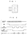
- By utilizing the feature for updating only the lower address, page mode access or static column access is proposed to shorten the DRAM access time. The operation for reading out three address signals (0100)H to (0102)H (Fig. 1), where H represents the hexadecimal notation according to page mode access, will be described with reference to the timing chart of Fig. 2. Upper address (01)H is input to the DRAM. In response to this address, row address strobe signal
RAS goes to level "0". All data corresponding to upper address (01)H is read out from memory cells in the DRAM. Lower address (00)H is then input to the DRAM. In response to this, column address strobe signalCAS goes to level "0". Only data corresponding to address (00)H is read out from the DRAM and output outside the DRAM. As a result, data A stored at address (0100)H is read out as output data. - Subsequently, second lower address (01)H is input to the DRAM. In response to this, signal
CAS goes to level "0". Since all the data corresponding to address (01)H in the DRAM has been accessed, only the data corresponding to this lower address is selected from the accessed data and output outside the DRAM. Therefore, data B stored at address (0101)H of the DRAM is read out. Similarly, data is sequentially selected and output in response to the lower address inputs and falling of signalCAS to level "0" in synchronism with each lower address input. - According to page mode access, once the upper address input is supplied to the DRAM, only different lower address inputs are supplied thereto to read out desired data. Therefore, the access time for the second and subsequent read operations can be shortened.
- Static column access employs the same addressing as that of page mode access. In addition, as shown in Fig. 2, signal
CAS is set to be continuously active (level "0") within the period for inputting a plurality of lower addresses. Since the logical level of signalCAS need not be repeatedly changed, data access can be achieved at a higher speed. - In order to achieve high-speed access, page mode access and static column access are based on the assumption that the upper address is not frequently updated. In other words, if the upper address is frequently updated, high-speed access cannot be performed.
- A conventional device (e.g., a CPU or a DMA controller) for accessing a memory does not have a function for discriminating whether or not the upper address is updated. As a result, the conventional CPU or DMA controller cannot employ a page mode access or static column access function assigned to the DRAM.
- Prior art document EP-A-0 025 801 (PANAFACOM) discloses a circuit arrangement that effectively discriminates whether or not the upper portion of the address is updated, but does not actually employ page mode memory access, so that at every memory cycle lower and upper portions of the address are sequentially supplied to the DRAM.
- It is an object of the present invention to provide a memory access control circuit capable of effectively utilizing page mode access or static column access to realize high-speed memory access when a CPU or DMA controller accesses a memory.
- In order to achieve the above object of the present invention, there is provided a memory access control circuit comprising a memory access circuit for output-ting memory address data consisting of upper and lower address signals to access a memory and for requesting updating of a memory address as needed, address retaining means for retaining the upper and lower address signals output from the memory access circuit and for updating the memory address by a predetermined value on the basis of a control signal, upper address detecting means for detecting a change in upper address signal output from the memory access circuit, address switching means for sequentially switching and outputting the upper and lower address signals retained by the address retaining means, an address bus to which multiplexed upper and lower address signals output from the address switching means are transferred, a memory for receiving the multiplexed upper and lower address signals from the address bus, and control means for controlling the address switching means, to send only the lower address signal onto the address bus when an output from the upper address detecting means represents no updating of the upper address signal, and to send the sequentially switched upper and lower address signals onto the address bus when the output from the upper address detecting means represents updating of the upper address, under the condition that new address data is output from the memory access circuit or the memory access circuit requests updating of the memory address.
- This invention can be more fully understood from the following detailed description when taken in conjunction with the accompanying drawings, in which:
- Fig. 1 is a memory map showing a state of data stored in a memory;
- Fig. 2 is a timing chart for explaining the read operation for reading out data from the memory;
- Fig. 3 is a block diagram of a memory access control circuit according to an embodiment of the present invention;
- Figs. 4 and 5 are timing charts for explaining the memory access control circuit in Fig. 3;
- Fig. 6 is a state trasition diagram of a timing control circuit in the memory access control circuit of Fig. 3;
- Fig. 7 is another state trasition diagram of the timing control circuit in the memory access control circuit of Fig. 3;
- Fig. 8 is a block diagram of a memory access control circuit according to another embodiment of the present invention; and
- Fig. 9 is a timing chart for explaining the operation of the memory access control circuit in Fig. 8.
- Fig. 3 is a block diagram showing a memory access control circuit according to an embodiment of the present invention. Referring to Fig. 3, reference numeral 11 denotes a memory access circuit (e.g., a CPU or a DMA controller) having a memory access function. Access circuit 11 generates upper address signal UA, Lower address signal LA, address strobe signal AS, and count-up control signal CU in order to access a memory.
- Upper and lower address signals UA and LA, address strobe signal AS and count-up control signal CU are supplied from memory access circuit 11 to address
counter 12.Counter 12 comprises upper andlower address counters counter 12 retains address signals UA and LA in response to strobe signal AS. Whencounter 12 receives signal CU, the retained value is updated by a predetermined value, e.g., incremented by one. Signals UA and LA retained incounter 12 are output as upper and lower memory address signals UMA and LMA, respectively. - Upper and lower memory address signals UMA and LMA are supplied from
address counter 12 tomultiplexer 13.Multiplexer 13 time-divisionally sends address signals UMA and LMA ontoaddress bus 14 in response to address switching signal ASE (to be described later). - Upper memory address signal LMA output from
address counter 12 is input toold address register 15. Upon reception of new address signal NA (to be described later), register 15 stores it as upper memory address signal UMA and outputs it as old address signal OMA. - Old address signal OMA and upper memory address UMA are input to address
comparator 16.Comparator 16 compares signal OMA with signal UMA and determines a coincidence therebetween. If a noncoincidence is established,comparator 16 generates noncoincidence signal NE. Signal NE is input totiming control circuit 17. -
Timing control circuit 17 also receives address strobe signal AS, count-up control signal CU, and reset signal RST.Control circuit 17 outputs address switching signal ASE, new address signal NA, row address strobe signalRSA , column address strobe signalCAS , and wait signal WAI on the basis of the above input signals. Signal WAI is input to memory access circuit 11. SignalsRAS andCAS are input toDRAM 18. -
DRAM 18 is connected toaddress bus 14.DRAM 18 and memory access circuit 11 are connected viadata bus 19. - The operation of the memory access control circuit having the arrangement described above will be described with reference to timing charts in Figs. 4 and 5.
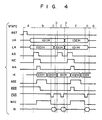
- The timing chart in Fig. 4 shows the sequence wherein memory access circuit 11 sequentially accesses three addresses (0100)H, (0101)H, and (0201)H after reset signal RST is input to
timing control circuit 17. - After reset signal RST is input, first data for address (0100)H is output from memory access circuit 11. In response to this address signal output, address strobe signal AS goes to level "1". The address output from access circuit 11 is divided into upper and lower address signals UA and LA. Signal UA has an address value of (01)H, and signal LA has an address value of (00)H. In response to address strobe signal AS,
address counter 12 retains these signals UA and LA. In this case, the address data is not retained inold address register 15, and its value is indefinite. For this reason, the result of comparison between signals UMA and OMA byaddress comparator 16 results in a noncoincidence, so thatcomparator 16 outputs noncoincidence signal NE. Since signal AS is input for the first time upon resetting,control circuit 17 outputs new address signal NA. Upon reception of signal NA, register 15 stores and retains address signal UMA having a value of (01)H. - After resetting, address switching signal ASE is set to be level "1" by timing
control circuit 17. When signal ASE goes to level "1",multiplexer 13 switches to upper memory address (01)H received fromaddress counter 12 during this period and outputs it ontoaddress bus 14. Subsequently, signal ASE is set at level "0" intiming control circuit 17. Then, multiplexer 13 switches to lower memory address (00)H received fromaddress counter 12 and outputs it ontoaddress bus 14. - As shown in Fig. 4, at timings when upper and lower address signals for addresses (01)H and (00)H are sent onto
address bus 14, signalsRAS andCAS sequentially go to level "0", thereby causingDRAM 18 to receive signals for addresses (01)H and (00)H. Thereafter, data is read out on the basis of the received upper and lower memory address signals. The readout data is transferred to memory access circuit 11 throughdata bus 19. - Subsequently, second data for address (0101)H is output from memory access circuit 11, and address strobe signal AS is output in response thereto. The address data is divided into upper and lower address signals UA and LA in the same manner as described above. However, at this time,
address register 15 retains signal UMA for previous upper memory address signal (01)H. This address signal UMA coincides with old address signal OMA, and addresscomparator 16 does not output noncoincidence signal NE. In this case,timing control circuit 17 does not output new address signal NA. The retained value ofregister 15 is kept unchanged. Incontrol circuit 17, address switching signal ASE is kept at level "0", and only signalCAS goes to level "0"Multiplexer 13 then switches to lower memory address (01)H received fromcounter 12 and outputs it ontoaddress bus 14. On the basis of signalCAS ,DRAM 18 receives signal LA for lower memory address (01)H. Thereafter, data is read out fromDRAM 18 by a combination of signals UA and LA, respectively, for upper and lower memory addresses (01)H and (01)H. The readout data is transferred to memory access circuit 11 viadata bus 19. -
DRAM 18 is accessed by outputting only lower memory address signal LMA ontoaddress bus 14 when upper address signal UA is not updated. - Third data for address (0201)H is output from memory access circuit 11. In this case, signal UA for upper address (02)H and signal LA for lower address (01)H are sent to address
counter 12.Old address register 15 retains signal UMA for previous upper memory address (01)H. No coincidence is established between signal UMA and old address OMA, and addresscomparator 16 outputs noncoincidence signal NE. Upon reception of signal NE,timing control circuit 17 outputs new address signal NA.Old address register 15 receives signal UMA for upper memory address and old address signal OMA is updated. Thereafter,control circuit 17 sets signalRAS to level "1", signifying that page mode access ofDRAM 18 has been completed. Incontrol circuit 17, address switching signal ASE is set at level "1", and then signalRAS goes to level "0" again, thus signifying that new page mode access ofDRAM 18 has started. While signal ASE is set at level "1",multiplexer 13 switches to signal UMA for upper memory address (02)H and outputs it ontoaddress bus 14.DRAM 18 receives signal UMA in response to signalRAS . Subsequently, intiming control circuit 17, address switching signal ASE goes to level "0". For the period of this logic level,multiplexer 13 switches to signal UMA for lower memory address (01)H received fromcounter 12 and outputs it ontoaddress bus 14. Thereafter, incontrol circuit 17, signal CAS goes to level "0".DRAM 18 receives signal LMA for lower memory address (01)H in response to signalCAS . Data is read out fromDRAM 18 by a combination of signals UA and LA, respectively, for upper and lower addresses (02)H and (01)H. The readout data is transferred to memory access circuit 11 viadata bus 19. -
Timing control circuit 17 outputs wait signal WAI whenmultiplexer 13 supplies upper memory address signal UMA ontoaddress bus 14, signalling to memory access circuit 11 that the access time ofDRAM 18 is prolonged. When signal WAI is input to memory access circuit 11, circuit 11 prolongs current upper and lower address signals UA and LA so as to compensate for the access time ofDRAM 18. - In this manner, when upper address signal UA is changed, new upper memory address signal UMA is input to
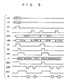
DRAM 18, and new page mode access is performed. - The timing chart in Fig. 5 explains the operation wherein memory access circuit 11 sequentially accesses successive addresses from (00FE)H.
- Memory access circuit 11 outputs first data for address (00FE)H and address strobe signal AS. This output operation is the same as that in the timing chart of Fig. 4, and a detailed description thereof will be omitted.
- In order to access the next address (00FF)H, count-up control signal CU is output from memory access circuit 11. When signal CU is received by timing
control circuit 17, the prestored address signal value is incremented by one inaddress counter 12. Signal LMA retained and output fromcounter 12 is updated from lower memory address (FE)H to lower memory address (FF)H. In this case, signal UM for upper memory address (00)H is not changed.Address comparator 16 does not output noncoincidence signal NE. For this reason, the same access as that using only lower memory address signal LMA (Fig. 4) is performed. - In order to access the next address (0100)H, memory access circuit 11 outputs count-up control signal CU.
Address counter 12 increments lower address signal LA value by one, so that address (FF)H is updated to (00)H. At the same time, a carry from the lower address causes updating of upper address (00)H to (01)H. Since the value of upper memory address signal UMA is changed, addresscomparator 16 outputs noncoincidence signal NE. The access operation is performed in the same manner as the case wherein higher memory address signal UAM is changed in the timing chart of Fig. 4. More specifically, new upper memory address signal UMA and lower memory address LMA are time-divisionally output to addressbus 14, and thusDRAM 18 is accessed. Thereafter, whenever the next address is accessed, memory access circuit 11 outputs count-up control signal CU. If address signal UMA is not changed upon incrementation of the retained value ofaddress counter 12, only address signal LMA is used to accessDRAM 18. However, if address signal UMA is changed, both new signal UMA and signal LMA are used to accessDRAM 18. - In successive addressing in the circuit of the above embodiment, upper memory address signal UMA is supplied to
DRAM 18 only when upper memory address signal UMA is changed. Otherwise, only lower memory address signal LMA is supplied toDRAM 18, thereby performing page mode access and hence achieving high-speed access ofDRAM 18. - Static column access for high-speed access of
DRAM 18 is different from page mode access in the manner of generating column address strobe control signalCAS . If updating of the memory address signal output from memory access circuit 11 can be detected,DRAM 18 can be accessed according to static column access. - Fig. 6 is a state trasition diagram of
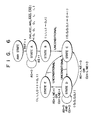
timing control circuit 17 by control page mode access. States A to E in Fig. 6 correspond to those in Fig. 2. The timings of various signals are shown in Fig. 4. In a given state, each signal is updated from logic "0" to logic "1", and vice versa. For illustrative convenience, if a signal takes logic "1" in the given state, it is simply represented by 1. If a signal does not take logic "1" in the given state, it is represented by 0. Since changes in logic levels of signalsRAS andCAS are very important,representations 0 → 1 or 1 → 0 are employed. Referring to Fig. 6, in any state, when reset signal RST is input (RST = 1), state A is initialized. In state A, various signals NA, ASE, WAI,RAS , andCAS are respectively set to be 0, 0, 0, 1, and 1. In state A, if signal AS is set at level "0" (AS = 0), state A continues. However, if signal AS is set at level "1" (AS = 1), state A is transited to state B. In state B, signals NA, ASE, WAI,RAS , andCAS are respectively set to be 1, 1, 1, 1 → 0, and 1. State B is unconditionally transited to state C. - In state C, signals NA, ASE, WAI,
RAS , andCAS are respectively set to be 0, 0, 0, 0, and 1 → 0 → 1. State C is unconditionally transited to state D. In state D, signals NA, ASE, WAI,RAS , andCAS are respectively set to be 0, 0, 0, 0, and 1. In state D, if signal AS is set at level "0" and signal CU is also set at level "0" (AS = 0 and CU = 0), state D continues. However, if AS = 1 and NE = 1 or if CU = 1 and NE = 1, state D is transited to state E. If AS = 1 and NE = 0 or if CU = 1 and NE = 0, state D is transited to state C. In state E, signals NA, ASE, WAI,RAS , andCAS are respectively set to be 1, 1, 1, 0 → 1 → 0, and 1. State E is unconditionally transited to state C. Control oftiming control circuit 17 is performed according to page mode access. - Fig. 7 is a state tradition diagram of
timing control circuit 17 so as to control static column mode access. Referring to Fig. 7, in any state, if reset signal RST is input, state A is initialized. In state A, signals NA, ASE, WAI,RAS , andCAS are respectively set to be 0, 0, 0, 1, and 1. In state A, if signal AS is set at level "0", state A continues. However, if signal AS goes to level "L", state A is transited to state B. In state B, signals NA, ASE, WAI,RAS , andCAS are respectively set to be 1, 1, 1, 1 → 0, and 1. State B is unconditionally transited to state C. - In state C, signals NA, ASE, WAI,
RAS , andCAS are respectively set to be 0, 0, 0, 0, and 0. State C is unconditionally shifted to state D. In state D, signals NA, ASE, WAI,RAS , andCAS are respectively set to be 0, 0, 0, 0, and 0. In state D, if signal AS is set at level "0" and signal CU is set at level "0" (AS = 0 and CU = 0), state D continues. However, if AS = 1 and NE = 1 or if CU = 1 and NE = 1, state D is transited to state E. If AS = 1 and NE = 0 or if CU = 1 and NE = 0, state D is transited to state F. In state E, signals NA, ASE, WAI,RAS , andCAS are respectively set to be 1, 1, 1, 0 → 1 → 0, and 0 → 1. State E is unconditionally transited to state C. In state F, signals NA, ASE, WAI,RAS , andCAS are respectively set to be 0, 0, 0, 0, and 0. State F is unconditionally transited to state D. In this manner, control oftiming control circuit 17 is performed according to static column mode access. - Fig. 8 is a block diagram of a memory access control circuit according to another embodiment of the present invention.
- The embodiment in Fig. 8 is different from that in Fig. 3 in the following points.
Address counter 22 capable of outputting outside the circuit carry output signal CO upon updating of the lower address signal is arranged in place ofaddress counter 12.Old address register 15 and addresscomparator 16 are omitted, and instead ORgate 23 is arranged to receive address strobe signal AS and carry signal CO fromcounter 22. Noncoincidence signal NE2 fromOR gate 23 is input totiming control circuit 27 used in place oftiming control circuit 17.Control circuit 27 receives address strobe signal AS, count-up control signal CU, and reset signal RST in addition to signal NE2. On the basis of these input signals,control circuit 27 generates address switching signal ASE, row address strobe signalRAS , column address strobe signalCAS , and wait signal WAI.Counter 22 comprises upper and lower address counters 22U and 22L. - The operation of the memory access control circuit having the arrangement described above will be described with reference to a timing chart of Fig. 9.
- First data of address (00FE)H from memory access circuit 11 is divided into upper and lower address signals UA and LA, and signals UMA and LMA are output therefrom. In response to these signals, access circuit 11 outputs address strobe signal AS. Signal AS is input to OR
gate 23 so thatgate 23 then outputs noncoincidence signal NE2. Whenever access circuit 11 outputs signal AS, ORgate 23 outputs signal NE2.Multiplexer 13 switches upper and lower address signals UMA and LMA for every signal NE2 so that address signals selectively appear onaddress bus 14.DRAM 18 receives address data on the basis of signalsRAS andCAS output from timingcontrol circuit 27. Data access is performed in response to such addressing. - If memory access circuit 11 accesses second data for address (00FF)H next to address (00FE)H, circuit 11 outputs only count-up control signal CU. Upon reception of signal CU, only the value of lower address signal LA is incremented by one in
address counter 22 so that the lower address is updated from (FE)H to (FF)H. In this case, no carry signal CO is generated bylower address counter 22L, and noncoincidence signal NE2 is not output fromOR gate 23. In the same manner as in the case wherein upper memory address signal UMA is not changed in the timing chart of Fig. 4,DRAM 18 is accessed by only lower memory address signal LMA. - Subsequently, when memory access circuit 11 outputs third data for address (0100)H next to address (00FF)H, access circuit 11 outputs only count-up control signal CU. Upon reception of signal CU, the value of lower address signal LA is incremented by one in
address counter 22 so that the lower address is updated from (FF)H to (00)H. In addition, carry signal CO fromlower address counter 22L updates the upper address from (00)H to (01)H. Since signal CO is input to ORgate 23, non-coincidence signal NE2 is output fromOR gate 23 later. In this case, in the same manner as in the case wherein upper memory address signal UMA is changed in the timing chart of Fig. 4, new upper memory address signal UMA and lower memory address signal LMA are time-divisionally output ontoaddress bus 14.DRAM 18 is thus accessed by new page mode access. - In the memory access control circuit of each embodiment described above, the upper address signal is supplied to a memory (e.g., a DRAM) using a multiplexed address signal only when the upper address is updated. Thus, the upper address signal is not output when the upper address is not updated. Therefore, page mode access or static column access for shortening access time can be performed. Furthermore, since retaining and incrementing means of the memory address are arranged, page mode access or static column access can be performed such that only the start address is specified to access succeeding addresses and thereafter count-up control signal CU, is output from memory access circuit 11.
- The present invention is not limited to the particular embodiments described above. Various changes and modifications may be made within the spirit and scope of the invention. In each embodiment described above, data read access for
DRAM 18 is exemplified. However, page mode access or static column access may be effectively utilized in the write mode ofDRAM 18 in the same manner as in the read mode. - In the embodiment of Fig. 3,
counter 12 has its count incremented by one every time it receives signal CU from memory access circuit 11. Instead, counter can be replaced by a incremented by any other value every time it receives signal CU, said value being determined by another signal from memory access circuit 11.
Claims (3)
- A memory access control circuit comprising:
a memory access circuit (11) for outputting memory address data consisting of upper and lower address data, an address strobe signal, and a count-up control signal for requesting the updating of a memory address, said upper address representing a memory row address, and said lower address representing a memory column address;
address retaining means (12, 22), responsive to said memory access circuit (11), including an upper address counter (12U, 22U) and a lower address counter (12L, 22L), for retaining said upper and lower address data, respectively, when said memory access circuit (11) outputs said address strobe signal, and for updating said retained memory address data by a predetermined value when said memory access circuit (11) outputs said count-up control signal;
upper address retaining means (15) for retaining the value of said upper address data retained in said upper address counter (12U, 22U) prior to the updating of said retained memory address data;
signal output means (16) for comparing said upper address data retained in said upper address counter (12U, 22U) with said upper address data retained by said upper address retaining means (15), and for outputting a non-coincidence signal when said compared addresses are not identical;
an address bus (14);
address switching means (13) for sequentially switching and outputting to said address bus (14) said upper and lower address data retained by said upper and lower address counters (12U, 22U; 12L, 22L);
a memory (18) for receiving from said address bus (14) said upper and lower address data output from said address switching means (13), said upper and lower address data being used as a row address signal and a column address signal, respectively; and
control means (17), operational in response to said address strobe signal or said count-up control signal for controlling said address switching means (13) to output said lower address data from said lower address counter (12L, 22L) to said address bus (14) when said signal output means (16) does not output said non-coincidence signal, and sequentially to output said upper and lower address data from said upper and lower address counters (12U, 22U; 12L, 22L) to said address bus (14) when said signal output means (16) outputs said non-coincidence signal, and for outputting a wait signal when said signal outputting means (16) outputs said non-coincidence signal, said wait signal causing said memory access circuit (11) to prolong the period during which said memory address data is output. - A circuit according to claim 1, characterized in that said memory (18) comprises a dynamic random access memory.
- A circuit according to claim 1 or 2, characterized in that said control means (17; 27) supplies a row address strobe signal to said memory (18) when the upper address signal for the memory address is transferred via said address bus (14) and a column address strobe signal to said memory (18) when the lower address signal for the memory address is transferred via said address bus (14).
Applications Claiming Priority (2)
| Application Number | Priority Date | Filing Date | Title |
|---|---|---|---|
| JP290209/85 | 1985-12-23 | ||
| JP60290209A JPS62149099A (en) | 1985-12-23 | 1985-12-23 | Memory access controlling circuit |
Publications (3)
| Publication Number | Publication Date |
|---|---|
| EP0226950A2 EP0226950A2 (en) | 1987-07-01 |
| EP0226950A3 EP0226950A3 (en) | 1990-01-17 |
| EP0226950B1 true EP0226950B1 (en) | 1993-02-17 |
Family
ID=17753159
Family Applications (1)
| Application Number | Title | Priority Date | Filing Date |
|---|---|---|---|
| EP86117189A Expired - Lifetime EP0226950B1 (en) | 1985-12-23 | 1986-12-10 | Memory access control circuit |
Country Status (4)
| Country | Link |
|---|---|
| US (1) | US4839856A (en) |
| EP (1) | EP0226950B1 (en) |
| JP (1) | JPS62149099A (en) |
| DE (1) | DE3687787T2 (en) |
Families Citing this family (31)
| Publication number | Priority date | Publication date | Assignee | Title |
|---|---|---|---|---|
| US5526506A (en) * | 1970-12-28 | 1996-06-11 | Hyatt; Gilbert P. | Computer system having an improved memory architecture |
| US5459846A (en) * | 1988-12-02 | 1995-10-17 | Hyatt; Gilbert P. | Computer architecture system having an imporved memory |
| WO1989001204A1 (en) * | 1987-07-23 | 1989-02-09 | Ncr Corporation | Memory access for a computer system |
| US5058005A (en) * | 1988-09-09 | 1991-10-15 | Compaq Computer Corporation | Computer system with high speed data transfer capabilities |
| US5159676A (en) * | 1988-12-05 | 1992-10-27 | Micron Technology, Inc. | Semi-smart DRAM controller IC to provide a pseudo-cache mode of operation using standard page mode draws |
| CA2011518C (en) * | 1989-04-25 | 1993-04-20 | Ronald N. Fortino | Distributed cache dram chip and control method |
| US5261073A (en) * | 1989-05-05 | 1993-11-09 | Wang Laboratories, Inc. | Method and apparatus for providing memory system status signals |
| US6564308B2 (en) | 1989-05-05 | 2003-05-13 | Samsung Electronics Co. Ltd. | Multiple mode memory module |
| JP2679296B2 (en) * | 1989-09-13 | 1997-11-19 | 日産自動車株式会社 | Kick down switch mounting structure |
| JPH03113794A (en) * | 1989-09-22 | 1991-05-15 | Toshiba Corp | Semiconductor memory device |
| US5276856A (en) * | 1989-09-28 | 1994-01-04 | Pixel Semiconductor, Inc. | Memory controller flexible timing control system and method |
| JP2925600B2 (en) * | 1989-11-07 | 1999-07-28 | 富士通株式会社 | Semiconductor storage device |
| US5280601A (en) * | 1990-03-02 | 1994-01-18 | Seagate Technology, Inc. | Buffer memory control system for a magnetic disc controller |
| JPH047761A (en) * | 1990-04-26 | 1992-01-13 | Fuji Xerox Co Ltd | Memory access method |
| JPH0682339B2 (en) * | 1990-08-31 | 1994-10-19 | インターナショナル・ビジネス・マシーンズ・コーポレイション | Memory access system and method |
| US5265236A (en) * | 1990-11-29 | 1993-11-23 | Sun Microsystems, Inc. | Method and apparatus for increasing the speed of memory access in a virtual memory system having fast page mode |
| US5253214A (en) * | 1991-09-27 | 1993-10-12 | Eastman Kodak Company | High-performance memory controller with application-programmable optimization |
| US5485589A (en) * | 1991-12-31 | 1996-01-16 | Dell Usa, L.P. | Predictive addressing architecture |
| JP2729126B2 (en) * | 1992-03-24 | 1998-03-18 | 富士通株式会社 | Address trace circuit of debug system |
| ATE144334T1 (en) * | 1992-06-04 | 1996-11-15 | Cabletron Systems Inc | ADAPTIVE STORAGE CONTROL DEVICE. |
| US5715421A (en) * | 1992-10-16 | 1998-02-03 | Seiko Epson Corporation | Apparatus and method of addressing paged mode memory including adjacent page precharging |
| JPH07281948A (en) * | 1994-04-06 | 1995-10-27 | Mitsubishi Electric Corp | Memory controller |
| US5594913A (en) * | 1994-09-16 | 1997-01-14 | Philips Electronics North America Corporation | High speed memory access system for a microcontroller with directly driven low order address bits |
| TW267222B (en) * | 1994-10-05 | 1996-01-01 | Ibm | Improved method and system of addressing |
| US5678017A (en) | 1995-03-24 | 1997-10-14 | Micron Technology, Inc. | Automatic reloading of serial read operation pipeline on last bit transfers to serial access memory in split read transfer operations |
| US5895480A (en) * | 1995-10-10 | 1999-04-20 | Holtek Microelectronics, Inc. | Method of and means for accessing an address by respectively substracting base addresses of memory integrated circuits from an access address |
| US6209071B1 (en) * | 1996-05-07 | 2001-03-27 | Rambus Inc. | Asynchronous request/synchronous data dynamic random access memory |
| JP3454094B2 (en) | 1997-07-22 | 2003-10-06 | 日本電気株式会社 | Shared memory control device and shared memory control method |
| US6263448B1 (en) | 1997-10-10 | 2001-07-17 | Rambus Inc. | Power control system for synchronous memory device |
| US6477630B2 (en) | 1999-02-24 | 2002-11-05 | International Business Machines Corporation | Hierarchical row activation method for banking control in multi-bank DRAM |
| TWI397855B (en) * | 2008-05-07 | 2013-06-01 | Sunplus Mmedia Inc | Method for reducing pin counts and microprocessor using the same |
Family Cites Families (10)
| Publication number | Priority date | Publication date | Assignee | Title |
|---|---|---|---|---|
| US4156905A (en) * | 1974-02-28 | 1979-05-29 | Ncr Corporation | Method and apparatus for improving access speed in a random access memory |
| JPS5916354B2 (en) * | 1978-10-17 | 1984-04-14 | 日本電信電話株式会社 | Storage device |
| JPS5943786B2 (en) * | 1979-03-30 | 1984-10-24 | パナフアコム株式会社 | Storage device access method |
| US4495565A (en) * | 1981-11-09 | 1985-01-22 | At&T Bell Laboratories | Computer memory address matcher and process |
| GB2112256B (en) * | 1981-11-18 | 1985-11-06 | Texas Instruments Ltd | Memory apparatus |
| US4546451A (en) * | 1982-02-12 | 1985-10-08 | Metheus Corporation | Raster graphics display refresh memory architecture offering rapid access speed |
| JPS593790A (en) * | 1982-06-30 | 1984-01-10 | Yokogawa Hokushin Electric Corp | Storage device using dynamic memory element |
| JPS60258792A (en) * | 1984-06-04 | 1985-12-20 | Toshiba Corp | Dynamic ram |
| JPS6199996A (en) * | 1984-10-19 | 1986-05-19 | Ricoh Co Ltd | Dynamic RAM control method |
| US4701843A (en) * | 1985-04-01 | 1987-10-20 | Ncr Corporation | Refresh system for a page addressable memory |
-
1985
- 1985-12-23 JP JP60290209A patent/JPS62149099A/en active Pending
-
1986
- 1986-12-10 EP EP86117189A patent/EP0226950B1/en not_active Expired - Lifetime
- 1986-12-10 DE DE8686117189T patent/DE3687787T2/en not_active Expired - Fee Related
- 1986-12-11 US US06/940,725 patent/US4839856A/en not_active Expired - Lifetime
Also Published As
| Publication number | Publication date |
|---|---|
| JPS62149099A (en) | 1987-07-03 |
| EP0226950A2 (en) | 1987-07-01 |
| EP0226950A3 (en) | 1990-01-17 |
| US4839856A (en) | 1989-06-13 |
| DE3687787T2 (en) | 1993-06-24 |
| DE3687787D1 (en) | 1993-03-25 |
Similar Documents
| Publication | Publication Date | Title |
|---|---|---|
| EP0226950B1 (en) | Memory access control circuit | |
| JPH0612863A (en) | Dual port DRAM | |
| JPH04293144A (en) | Computer system | |
| US4575796A (en) | Information processing unit | |
| US6292853B1 (en) | DMA controller adapted for transferring data in two-dimensional mapped address space | |
| KR920003699B1 (en) | Register circuit | |
| JPS63191397A (en) | Information processor | |
| JP3947856B2 (en) | Data setting control device | |
| JP2627370B2 (en) | Development support system | |
| KR0165505B1 (en) | Communication device using shared memory | |
| JPH0689237A (en) | Memory control system | |
| SU1487101A1 (en) | DEVICE FOR MANAGING THE DYNAMIC MEMORY REGENERATION | |
| KR900009212Y1 (en) | Address controller | |
| JPH04153984A (en) | Method for controlling dynamic memory | |
| JP2590695B2 (en) | Time division switch circuit | |
| JPS585434B2 (en) | display device | |
| JPH07191099A (en) | IC inspection device | |
| JPH0830434A (en) | Memory access controller | |
| JPH0797814B2 (en) | Memory controller | |
| JPH06231037A (en) | Address generation circuit to extend address | |
| JPH0668540B2 (en) | Semiconductor memory test equipment | |
| JPH11176155A (en) | Dram-refreshing circuit | |
| JPH05135571A (en) | Memory controller | |
| JPH02166547A (en) | Information processor | |
| JPH02137040A (en) | Image processing device |
Legal Events
| Date | Code | Title | Description |
|---|---|---|---|
| PUAI | Public reference made under article 153(3) epc to a published international application that has entered the european phase |
Free format text: ORIGINAL CODE: 0009012 |
|
| 17P | Request for examination filed |
Effective date: 19870107 |
|
| AK | Designated contracting states |
Kind code of ref document: A2 Designated state(s): DE FR GB |
|
| PUAL | Search report despatched |
Free format text: ORIGINAL CODE: 0009013 |
|
| AK | Designated contracting states |
Kind code of ref document: A3 Designated state(s): DE FR GB |
|
| 17Q | First examination report despatched |
Effective date: 19910426 |
|
| GRAA | (expected) grant |
Free format text: ORIGINAL CODE: 0009210 |
|
| AK | Designated contracting states |
Kind code of ref document: B1 Designated state(s): DE FR GB |
|
| REF | Corresponds to: |
Ref document number: 3687787 Country of ref document: DE Date of ref document: 19930325 |
|
| ET | Fr: translation filed | ||
| PLBE | No opposition filed within time limit |
Free format text: ORIGINAL CODE: 0009261 |
|
| STAA | Information on the status of an ep patent application or granted ep patent |
Free format text: STATUS: NO OPPOSITION FILED WITHIN TIME LIMIT |
|
| 26N | No opposition filed | ||
| PGFP | Annual fee paid to national office [announced via postgrant information from national office to epo] |
Ref country code: GB Payment date: 19971201 Year of fee payment: 12 |
|
| PGFP | Annual fee paid to national office [announced via postgrant information from national office to epo] |
Ref country code: FR Payment date: 19971209 Year of fee payment: 12 |
|
| PGFP | Annual fee paid to national office [announced via postgrant information from national office to epo] |
Ref country code: DE Payment date: 19971222 Year of fee payment: 12 |
|
| PG25 | Lapsed in a contracting state [announced via postgrant information from national office to epo] |
Ref country code: GB Free format text: LAPSE BECAUSE OF NON-PAYMENT OF DUE FEES Effective date: 19981210 |
|
| GBPC | Gb: european patent ceased through non-payment of renewal fee |
Effective date: 19981210 |
|
| PG25 | Lapsed in a contracting state [announced via postgrant information from national office to epo] |
Ref country code: FR Free format text: LAPSE BECAUSE OF NON-PAYMENT OF DUE FEES Effective date: 19990831 |
|
| REG | Reference to a national code |
Ref country code: FR Ref legal event code: ST |
|
| PG25 | Lapsed in a contracting state [announced via postgrant information from national office to epo] |
Ref country code: DE Free format text: LAPSE BECAUSE OF NON-PAYMENT OF DUE FEES Effective date: 19991001 |