EP0225592B1 - Procédé de recristallisation de films conducteurs - Google Patents
Procédé de recristallisation de films conducteurs Download PDFInfo
- Publication number
- EP0225592B1 EP0225592B1 EP86116778A EP86116778A EP0225592B1 EP 0225592 B1 EP0225592 B1 EP 0225592B1 EP 86116778 A EP86116778 A EP 86116778A EP 86116778 A EP86116778 A EP 86116778A EP 0225592 B1 EP0225592 B1 EP 0225592B1
- Authority
- EP
- European Patent Office
- Prior art keywords
- layer
- region
- nonmonocrystalline
- thermal
- film
- Prior art date
- Legal status (The legal status is an assumption and is not a legal conclusion. Google has not performed a legal analysis and makes no representation as to the accuracy of the status listed.)
- Expired - Lifetime
Links
- VYPSYNLAJGMNEJ-UHFFFAOYSA-N Silicium dioxide Chemical compound O=[Si]=O VYPSYNLAJGMNEJ-UHFFFAOYSA-N 0.000 claims description 49
- 229910021420 polycrystalline silicon Inorganic materials 0.000 claims description 46
- 229920005591 polysilicon Polymers 0.000 claims description 44
- 238000000034 method Methods 0.000 claims description 37
- 235000012239 silicon dioxide Nutrition 0.000 claims description 24
- 239000000377 silicon dioxide Substances 0.000 claims description 24
- 239000004065 semiconductor Substances 0.000 claims description 21
- XUIMIQQOPSSXEZ-UHFFFAOYSA-N Silicon Chemical compound [Si] XUIMIQQOPSSXEZ-UHFFFAOYSA-N 0.000 claims description 17
- 229910052710 silicon Inorganic materials 0.000 claims description 17
- 239000010703 silicon Substances 0.000 claims description 17
- 239000000758 substrate Substances 0.000 claims description 15
- 229910052581 Si3N4 Inorganic materials 0.000 claims description 12
- HQVNEWCFYHHQES-UHFFFAOYSA-N silicon nitride Chemical compound N12[Si]34N5[Si]62N3[Si]51N64 HQVNEWCFYHHQES-UHFFFAOYSA-N 0.000 claims description 12
- 230000003667 anti-reflective effect Effects 0.000 claims description 7
- 239000000463 material Substances 0.000 claims description 7
- 239000012212 insulator Substances 0.000 claims description 6
- 230000001678 irradiating effect Effects 0.000 claims description 5
- XKRFYHLGVUSROY-UHFFFAOYSA-N argon Substances [Ar] XKRFYHLGVUSROY-UHFFFAOYSA-N 0.000 claims description 4
- XAGFODPZIPBFFR-UHFFFAOYSA-N aluminium Chemical compound [Al] XAGFODPZIPBFFR-UHFFFAOYSA-N 0.000 claims description 3
- 229910052782 aluminium Inorganic materials 0.000 claims description 3
- 229910052786 argon Inorganic materials 0.000 claims description 3
- 238000009736 wetting Methods 0.000 claims description 3
- -1 argon ion Chemical class 0.000 claims description 2
- 230000001590 oxidative effect Effects 0.000 claims description 2
- 239000004411 aluminium Substances 0.000 claims 1
- 229910052814 silicon oxide Inorganic materials 0.000 claims 1
- 238000005516 engineering process Methods 0.000 description 15
- 238000010438 heat treatment Methods 0.000 description 15
- 239000004020 conductor Substances 0.000 description 11
- 238000001953 recrystallisation Methods 0.000 description 10
- 238000010521 absorption reaction Methods 0.000 description 3
- 238000000862 absorption spectrum Methods 0.000 description 3
- 230000003247 decreasing effect Effects 0.000 description 3
- 238000004518 low pressure chemical vapour deposition Methods 0.000 description 3
- 230000008018 melting Effects 0.000 description 3
- 238000002844 melting Methods 0.000 description 3
- 238000001020 plasma etching Methods 0.000 description 3
- KRHYYFGTRYWZRS-UHFFFAOYSA-N Fluorane Chemical compound F KRHYYFGTRYWZRS-UHFFFAOYSA-N 0.000 description 2
- NBIIXXVUZAFLBC-UHFFFAOYSA-N Phosphoric acid Chemical compound OP(O)(O)=O NBIIXXVUZAFLBC-UHFFFAOYSA-N 0.000 description 2
- 238000000295 emission spectrum Methods 0.000 description 2
- 239000007789 gas Substances 0.000 description 2
- 229960002050 hydrofluoric acid Drugs 0.000 description 2
- 239000000203 mixture Substances 0.000 description 2
- 230000006911 nucleation Effects 0.000 description 2
- 238000010899 nucleation Methods 0.000 description 2
- 230000002093 peripheral effect Effects 0.000 description 2
- 238000001947 vapour-phase growth Methods 0.000 description 2
- XPDWGBQVDMORPB-UHFFFAOYSA-N Fluoroform Chemical compound FC(F)F XPDWGBQVDMORPB-UHFFFAOYSA-N 0.000 description 1
- GRYLNZFGIOXLOG-UHFFFAOYSA-N Nitric acid Chemical compound O[N+]([O-])=O GRYLNZFGIOXLOG-UHFFFAOYSA-N 0.000 description 1
- 229910000147 aluminium phosphate Inorganic materials 0.000 description 1
- 238000006243 chemical reaction Methods 0.000 description 1
- 238000005229 chemical vapour deposition Methods 0.000 description 1
- 239000013078 crystal Substances 0.000 description 1
- 229910021419 crystalline silicon Inorganic materials 0.000 description 1
- 230000004927 fusion Effects 0.000 description 1
- 150000002500 ions Chemical class 0.000 description 1
- 238000004093 laser heating Methods 0.000 description 1
- 238000012986 modification Methods 0.000 description 1
- 230000004048 modification Effects 0.000 description 1
- 229910017604 nitric acid Inorganic materials 0.000 description 1
- 230000003287 optical effect Effects 0.000 description 1
- 238000000059 patterning Methods 0.000 description 1
- 230000001737 promoting effect Effects 0.000 description 1
- 238000004544 sputter deposition Methods 0.000 description 1
- 230000009466 transformation Effects 0.000 description 1
- 230000001131 transforming effect Effects 0.000 description 1
- 238000001771 vacuum deposition Methods 0.000 description 1
Images


Classifications
-
- H—ELECTRICITY
- H01—ELECTRIC ELEMENTS
- H01L—SEMICONDUCTOR DEVICES NOT COVERED BY CLASS H10
- H01L21/00—Processes or apparatus adapted for the manufacture or treatment of semiconductor or solid state devices or of parts thereof
- H01L21/02—Manufacture or treatment of semiconductor devices or of parts thereof
- H01L21/04—Manufacture or treatment of semiconductor devices or of parts thereof the devices having potential barriers, e.g. a PN junction, depletion layer or carrier concentration layer
- H01L21/18—Manufacture or treatment of semiconductor devices or of parts thereof the devices having potential barriers, e.g. a PN junction, depletion layer or carrier concentration layer the devices having semiconductor bodies comprising elements of Group IV of the Periodic Table or AIIIBV compounds with or without impurities, e.g. doping materials
- H01L21/26—Bombardment with radiation
- H01L21/263—Bombardment with radiation with high-energy radiation
- H01L21/268—Bombardment with radiation with high-energy radiation using electromagnetic radiation, e.g. laser radiation
-
- H—ELECTRICITY
- H01—ELECTRIC ELEMENTS
- H01L—SEMICONDUCTOR DEVICES NOT COVERED BY CLASS H10
- H01L21/00—Processes or apparatus adapted for the manufacture or treatment of semiconductor or solid state devices or of parts thereof
- H01L21/02—Manufacture or treatment of semiconductor devices or of parts thereof
- H01L21/02104—Forming layers
- H01L21/02365—Forming inorganic semiconducting materials on a substrate
- H01L21/02656—Special treatments
- H01L21/02664—Aftertreatments
- H01L21/02667—Crystallisation or recrystallisation of non-monocrystalline semiconductor materials, e.g. regrowth
- H01L21/02675—Crystallisation or recrystallisation of non-monocrystalline semiconductor materials, e.g. regrowth using laser beams
-
- H—ELECTRICITY
- H01—ELECTRIC ELEMENTS
- H01L—SEMICONDUCTOR DEVICES NOT COVERED BY CLASS H10
- H01L21/00—Processes or apparatus adapted for the manufacture or treatment of semiconductor or solid state devices or of parts thereof
- H01L21/02—Manufacture or treatment of semiconductor devices or of parts thereof
- H01L21/02104—Forming layers
- H01L21/02107—Forming insulating materials on a substrate
- H01L21/02109—Forming insulating materials on a substrate characterised by the type of layer, e.g. type of material, porous/non-porous, pre-cursors, mixtures or laminates
- H01L21/02112—Forming insulating materials on a substrate characterised by the type of layer, e.g. type of material, porous/non-porous, pre-cursors, mixtures or laminates characterised by the material of the layer
- H01L21/02123—Forming insulating materials on a substrate characterised by the type of layer, e.g. type of material, porous/non-porous, pre-cursors, mixtures or laminates characterised by the material of the layer the material containing silicon
- H01L21/02164—Forming insulating materials on a substrate characterised by the type of layer, e.g. type of material, porous/non-porous, pre-cursors, mixtures or laminates characterised by the material of the layer the material containing silicon the material being a silicon oxide, e.g. SiO2
-
- H—ELECTRICITY
- H01—ELECTRIC ELEMENTS
- H01L—SEMICONDUCTOR DEVICES NOT COVERED BY CLASS H10
- H01L21/00—Processes or apparatus adapted for the manufacture or treatment of semiconductor or solid state devices or of parts thereof
- H01L21/02—Manufacture or treatment of semiconductor devices or of parts thereof
- H01L21/02104—Forming layers
- H01L21/02365—Forming inorganic semiconducting materials on a substrate
- H01L21/02367—Substrates
- H01L21/0237—Materials
- H01L21/02373—Group 14 semiconducting materials
- H01L21/02381—Silicon, silicon germanium, germanium
-
- H—ELECTRICITY
- H01—ELECTRIC ELEMENTS
- H01L—SEMICONDUCTOR DEVICES NOT COVERED BY CLASS H10
- H01L21/00—Processes or apparatus adapted for the manufacture or treatment of semiconductor or solid state devices or of parts thereof
- H01L21/02—Manufacture or treatment of semiconductor devices or of parts thereof
- H01L21/02104—Forming layers
- H01L21/02365—Forming inorganic semiconducting materials on a substrate
- H01L21/02436—Intermediate layers between substrates and deposited layers
- H01L21/02439—Materials
- H01L21/02488—Insulating materials
-
- H—ELECTRICITY
- H01—ELECTRIC ELEMENTS
- H01L—SEMICONDUCTOR DEVICES NOT COVERED BY CLASS H10
- H01L21/00—Processes or apparatus adapted for the manufacture or treatment of semiconductor or solid state devices or of parts thereof
- H01L21/02—Manufacture or treatment of semiconductor devices or of parts thereof
- H01L21/02104—Forming layers
- H01L21/02365—Forming inorganic semiconducting materials on a substrate
- H01L21/02518—Deposited layers
- H01L21/02521—Materials
- H01L21/02524—Group 14 semiconducting materials
- H01L21/02532—Silicon, silicon germanium, germanium
-
- H—ELECTRICITY
- H01—ELECTRIC ELEMENTS
- H01L—SEMICONDUCTOR DEVICES NOT COVERED BY CLASS H10
- H01L21/00—Processes or apparatus adapted for the manufacture or treatment of semiconductor or solid state devices or of parts thereof
- H01L21/02—Manufacture or treatment of semiconductor devices or of parts thereof
- H01L21/02104—Forming layers
- H01L21/02365—Forming inorganic semiconducting materials on a substrate
- H01L21/02518—Deposited layers
- H01L21/02587—Structure
- H01L21/0259—Microstructure
- H01L21/02595—Microstructure polycrystalline
-
- H—ELECTRICITY
- H01—ELECTRIC ELEMENTS
- H01L—SEMICONDUCTOR DEVICES NOT COVERED BY CLASS H10
- H01L21/00—Processes or apparatus adapted for the manufacture or treatment of semiconductor or solid state devices or of parts thereof
- H01L21/02—Manufacture or treatment of semiconductor devices or of parts thereof
- H01L21/02104—Forming layers
- H01L21/02365—Forming inorganic semiconducting materials on a substrate
- H01L21/02656—Special treatments
- H01L21/02664—Aftertreatments
- H01L21/02667—Crystallisation or recrystallisation of non-monocrystalline semiconductor materials, e.g. regrowth
- H01L21/02675—Crystallisation or recrystallisation of non-monocrystalline semiconductor materials, e.g. regrowth using laser beams
- H01L21/02683—Continuous wave laser beam
-
- H—ELECTRICITY
- H01—ELECTRIC ELEMENTS
- H01L—SEMICONDUCTOR DEVICES NOT COVERED BY CLASS H10
- H01L21/00—Processes or apparatus adapted for the manufacture or treatment of semiconductor or solid state devices or of parts thereof
- H01L21/02—Manufacture or treatment of semiconductor devices or of parts thereof
- H01L21/02104—Forming layers
- H01L21/02365—Forming inorganic semiconducting materials on a substrate
- H01L21/02656—Special treatments
- H01L21/02664—Aftertreatments
- H01L21/02667—Crystallisation or recrystallisation of non-monocrystalline semiconductor materials, e.g. regrowth
- H01L21/02691—Scanning of a beam
Definitions
- the present invention relates to the recrystallization of conductive material films, including semiconductor films.
- the present invention finds application in SOI (Silicon on Insulator) technology.
- SOI technology has been proposed as a means for providing high-speed and high-voltage semiconductor integrated circuits (ICs) and at present appears to be one of the most promising prospects for the realization of three-dimensional semiconductor integrated circuits.
- a polysilicon film In SOI technology, a polysilicon film, usually formed on an insulating layer such as a thermally-oxidized layer of a silicon substrate, is recrystallized, so as to end up single crystalline or grain-boundary free, using irradiation by a radiant energy beam such as a laser.
- a radiant energy beam such as a laser.
- nucleation in the polysilicon film during recrystallization must be controlled so as to be initiated at a single point in a molten region of the polysilicon film. This can be achieved by producing a temperature distribution, in a region to be recrystallized, having a profile which affords the lowest temperature at the center of the region and higher and higher temperatures towards the periphery of the region.
- the anti-reflective film produces a desired temperature profile which affords a lowest temperature at the center of each region corresponding to the apertures.
- any desired portion of a polysilicon film can be transformed into a single crystalline region of a desired size.
- the methods mentioned above can be categorized as direct-heating-type SOI technology.
- the polysilicon film formed on an insulating layer is patterned to provide islands prior to the recrystallization.
- the size of each island must be large enough to include therein the source and drain regions together with the active region, i.e. channel region, of a transistor.
- a region to be recrystallized is as small as possible when a desired temperature profile is established therein. Accordingly, it is desirable to selectively recrystallize only a small region, corresponding to an active region of a device, e.g. the channel region of a transistor, and to leave other regions, corresponding to source and drain regions of the transistor, in a polycrystalline state.
- the previous indirect-heating SOI technology is unable to selectively recrystallize only a region as small as a channel region in a polycrystalline island.
- a process of forming a semiconductor device comprising the successive steps of:- forming a nonmonocrystalline film of a semiconductor material on a major surface of an insulator; forming a thermal-conduction-controlling layer over the nonmonocrystalline film, said thermal-conduction-controlling layer having at least one portion of increased thickness defining a region in which the nonmonocrystalline film is to be recrystallized; forming a cap layer on said thermal-conduction-controlling layer; and irradiating the cap layer with an energy beam of radiant energy of a wavelength absorbed by said cap layer sufficient to melt said defined region of said nonmonocrystalline film; and allowing said nonmonocrystalline layer to cool, hence forming a grain-boundary-free recrystallised region in said defined region.
- a method of recrystallizing a region of a nonmonocrystalline conductive layer comprising the successive steps of:- forming a thermal-conduction-controlling layer on said nonmonocrystalline layer, the thermal-conduction-controlling layer having a portion of increased thickness above and defining said region of the nonmonocrystalline conductive layer; forming a cap layer above said thermal-conduction-controlling layer; and irradiating said cap layer with an energy beam of a wavelength absorbed by said cap layer such that said region of said nonmonocrystalline layer is melted; allowing said nonmonocrystalline layer to cool, hence forming a grain-boundary-free recrystallized region in said defined region.
- An embodiment of the present invention can provide a method for selectively transforming regions of a polycrystalline film of a conductive material into grain-boundary-free regions, in an indirect-heating SOI environment.
- An embodiment of the present invention can provide a process which can improve the yield of integrated circuit devices fabricated based on SOI.
- An embodiment of the present invention provides a process comprising steps of: forming a nonmonocrystalline film of a conductive material (for example semiconductor material such as polysilicon) on an insulator; forming a thermal-conduction-controlling layer of silicon dioxide, for example, on the nonmonocrystalline film, the thermal-conduction-controlling layer having thickness selectively increased at each portion thereof corresponding to predefined regions of the nonmonocrystalline film; forming an energy-absorbing cap layer of polysilicon, for example, on the thermal-conduction-controlling layer; and irradiating the energy-absorbing cap layer with an energy beam of radiant energy sufficient to melt and transform the nonmonocrystalline film in the predefined regions to be grain-boundary free by the heat generated in the energy-absorbing cap layer.
- a conductive material for example semiconductor material such as polysilicon
- Fig. 1 illustrates a recrystallization method according to a previously proposed indirect-heating SOI technology.
- an insulating film 52 is formed on a silicon substrate 51 and a polysilicon island 53 having a size corresponding to a semiconductor element, such as a transistor, to be fabricated therein is formed on the insulating film 52 through conventional vapour-phase growth and patterning techniques.
- a separating layer 54 is formed to cover the polysilicon island 53 and then a laser-absorbing layer 55 of polysilicon, for example, is formed on the insulating film 52, having thereon the polysilicon island 53, using a vapour-phase growth technique.
- the separating layer 54 is for preventing fusion of polysilicon island 53 and laser-absorbing layer 55.
- the laser-absorbing layer 55 is irradiated with a radiant energy beam 56, such as an argon (Ar) ion laser beam, having an emission spectrum almost equal to the absorption spectrum of the polysilicon constituting the laser-absorption layer 55.
- a radiant energy beam 56 such as an argon (Ar) ion laser beam
- Ar argon
- the laser-absorbing layer 55 is irradiated with a radiant energy beam 56, such as an argon (Ar) ion laser beam, having an emission spectrum almost equal to the absorption spectrum of the polysilicon constituting the laser-absorption layer 55.
- grain boundaries sometimes occur in a few out of many thousands of islands, for example, formed on an integrated circuit chip, because each of the islands (such as the island 53) has a size as great as 2 ⁇ 10 ⁇ 5 m by 6 ⁇ 10 ⁇ 5 m (20 ⁇ 60 square-microns) in order to contain regions which will provide source and drain of a transistor, and hence, the temperature distribution formed therein is apt to deviate from a desired profile, as mentioned above.
- Fig. 2 is a schematic sectional elevational view illustrating an embodiment of the present invention.
- a conductive material film 2 a semiconductor film for example, is formed on an insulating film 1, and then a thermal-conduction-controlling layer (simply referred to as a TCC layer, hereinafter) 5 is formed on the conductive material film 2.
- the TCC layer 5 has a selectively-increased-thickness portion 4 corresponding to a region 3 at which a portion 8 of the conductive material film 2 is to be transformed so as to be grain-boundary free.
- an energy-absorbing cap layer 6 is formed on the TCC layer 5 and the energy-absorbing cap layer 6 is irradiated with a radiant energy beam 7.
- the conductive material film 2 is melted by heat transferred from the energy-absorbing layer 6 and recrystallized.
- the TCC layer 5 is usually composed of a material having a thermal conductivity relatively smaller than that of the energy-absorbing cap layer 6, and further, that of the conductive material layer 2.
- Heat flowing from the energy-absorbing cap layer 6 to the conductive material film 2 is restricted by the TCC layer 5, particularly in the region 3.
- the temperature of the conductive material film 2 is lower in the region 3 than in surrounding regions.
- a temperature distribution is established which provides a lowest temperature at the center of the region, with temperature becoming higher and higher towards the periphery of the region.
- the region 3 is transformed into a grain-boundary-free single-crystalline region. It will be clear that there is substantially no lower limit of the size of the region 3. Therefore, the region can be designed to be as small as the channel region of a transistor. This means that the probability of existence of a grain boundary in the recrystallized region 3 can be substantially decreased compared with that for a recrystallized island 53 provided as illustrated in Fig. 1 in accordance with the previously proposed method.
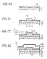
- Figs. 3A-3G are respective schematic sectional elevational views illustrating steps in a process embodying the present invention.
- Like reference signs designate like or corresponding parts throughout.
- a relatively thick lower insulating film 12 such as a silicon dioxide (SiO2) film of 1 ⁇ 10 ⁇ 6 m - 2 ⁇ 10 ⁇ 6 m (1-2 microns) thickness, is formed on a silicon substrate 11 by thermally oxidizing the substrate, for example. Then, a polysilicon film 13 having a thickness of about 400 nm (4000 ⁇ ) is formed on the lower insulating film 12 using conventional low-pressure chemical vapour deposition (LP-CVD), for example.
- LP-CVD low-pressure chemical vapour deposition
- SiO2 layer having a thickness of about 400 nm (4000 ⁇ ) is formed on the polysilicon film 13 using a conventional CVD method.
- the SiO2 layer is patterned by a conventional reactive ion etching technique using a not-shown resist mask and etchant, CHF3 gas, for example.
- a SiO2 layer pattern 14 is selectively formed to cover the polysilicon film 13 in region 3, in which the polysilicon film 13 is to be transformed to be grain-boundary free.
- the region 3 is defined as (destined to be) an active region, e.g. channel region of a transistor, and has an area of as little as 2 ⁇ 10 ⁇ 5m by 2 ⁇ 10 ⁇ 5m (20 ⁇ 20 square-microns).
- the exposed surface 4 of the polysilicon film 13 around the SiO2 layer pattern 14 is thermally oxidized so as to form another SiO2 layer 15, of 300A thickness for example, as shown in Fig. 3B.
- the SiO2 layer 15 has the role of preventing chemical reaction between the polysilicon film 13 and the Si3N4 layer 16 at high temperature, and the Si3N4 layer 16 has the role of promoting wetting of a laser absorbing layer of polysilicon, which is formed thereon later, to the substrate.
- an energy-absorbing layer 17 of polysilicon for example, of 700 nm (7000 ⁇ ) thickness is formed on the substrate having the TCC layer 5, using a conventional LP-CVD technique.
- an anti-reflective film 18 for a laser beam a Si3N4 film 18a and a SiO2 film 18b, each having a thickness of about 30 nm (300 ⁇ ), are successively formed on the polysilicon energy-absorbing layer 17, as shown in Fig. 3D.
- a radiant energy beam 7 is scanned over the polysilicon energy-absorbing layer 17 with preliminary heating applied to the substrate, and thus, the energy-absorbing layer 17 is heated up to a high temperature of about 1500-1600°C.
- An Ar-ion laser which outputs a beam of 500 nanometer wavelength, for example, is desirably used as the source of the radiant energy beam 7, since silicon reveals strong absorption at this wavelength.
- the laser beam is tuned so as to provide a Gaussian type intensity distribution in the spot of irradiation provided by the beam.
- the size of the spot must be large enough to encompass the predefined region of the polysilicon film 13 so that the polysilicon film 13 in the predefined region (2 ⁇ 10 ⁇ 5m by 2 ⁇ 10 ⁇ 5m or 20 ⁇ 20 square-microns) is melted by a single scan of the laser beam 7.
- Exemplary conditions for the laser beam irradiation are summarized as follows:-
- the polysilicon film 13 is melted by the heat transferred from the energy-absorbing layer 17 by conduction via the TCC layer 5.
- the energy-absorbing layer 17 of polysilicon is also melted.
- the heat flowing into the polysilicon film 13 under the SiO2 layer pattern 14, i.e. the large-thickness portion 4, of the TCC layer 5 is less at the central portion as compared with that at the peripheral portion, as mentioned before.
- a temperature distribution is established in the polysilicon film 13 in the predefined region having a profile providing the lowest temperature at the center with temperature becoming higher towards the periphery. Accordingly, recrystallization of the polysilicon film 13 proceeds to spread from the lowest temperature central portion to the peripheral portion, and thus, a grain boundary-free region 213 is formed in the recrystallized silicon film 113.
- the Si3N4 film 18a and SiO2 film 18b constituting an anti-reflective layer, are removed using respective conventional etchants; a phosphoric-acid-type solution for the Si3N4 film 18a and a fluoric-acid-type solution for the SiO2 film 18b, for example.
- the polysilicon energy-absorbing layer 17 is removed by using a conventional etchant such as a mixture of fluoric acid and nitric acid solutions, and then, the Si3N4 layer 16 and SiO2 layers 15 and 14 are removed by using respective conventional etchants; a phosphoric acid solution for the Si3N4 layer 16 and a fluoric acid solution for the SiO2 layers 15 and 14.
- the TCC layer 5 is removed and the recrystallized silicon film 113 including the predefined region 213 which has been selectively transformed to be grain-boundary-free is exposed as shown in Fig. 3F.
- the recrystallized silicon film 113 is patterned by a conventional RIE (reactive ion etching) technique incorporating a not-shown resist mask and an etchant such as a gas mixture of CF4 + O2, for example, and an island 19 of the recrystallized silicon film 113 including the grain-boundary-free region 213 is formed on the SiO2 lower insulating layer 12.
- RIE reactive ion etching
- a semiconductor circuit element such as a transistor is formed in the silicon island 19, wherein the active region of the element, such as the channel region of a transistor, is allocated in the grain-boundary-free region 213 and source and drain regions of the transistor are fabricated in the recrystallized silicon region 113 around the grain-boundary-free region 213.
- an integrated circuit having an SOI structure is provided.
- the recrystallized silicon island 19 has a size of 2 ⁇ 10 ⁇ 5m by 6 ⁇ 10 ⁇ 5m (20 ⁇ 60 square-microns), for example, the same as that of the silicon island 53 shown in Fig. 1 in relation to the previous proposal.
- a smaller region, such as the active region of a transistor, formed in the island is selectively transformed to be grain-boundary-free. Therefore, the probability of existence of a grain boundary in the active region is substantially decreased, and hence, the yield of SOI ICs can be increased.
- the shape of island need not be simple (e.g. rectangular) but can be complicated, for example with the structure of letters C, E, H and so forth, wherein a desired number of active regions can be formed in the structure.
- a recrystallization method embodying the present invention can be applied to a metallized layer of an integrated circuit. That is, a wiring layer such as one formed from amorphous aluminum, fabricated by a vacuum deposition or sputtering technique, for example, can be selectively transformed into a grain-boundary-free aluminum layer. Such a grain-boundary-free wiring layer can eliminate a type of disconnection which occurs in wiring lines for large current load due to existence of grain boundaries therein.
- the SiO2 film 15 and Si3N4 film 16 and the anti-reflective layer 18 shown in Fig. 3D are not essential.
- the energy-absorbing layer 17 in Fig. 3D need not be of polysilicon: that layer may be of other materials, provided matching of the wavelengths is established between the emission spectra of the laser beam and the absorption spectra of the energy-absorbing layer, wherein the other materials may have a higher melting point than that of the film to be recrystallized.
- An embodiment of the present invention provides a process allowing so-called indirect-heating SOI methodology to selectively transform predefined regions of a semiconductor film formed on an insulating substrate into grain-boundary-free regions.
- a semiconductor film which is recrystallized to be grain-boundary-free is heated above its melting point by the heat generated in an energy-absorbing layer formed thereon.
- a layer having a relatively smaller thermal conductivity such as a SiO2 layer, is provided between the semiconductor film to be recrystallized and the energy-absorbing layer, both having larger thermal conductivities.
- the smaller-thermal-conductivity layer functioning as a thermal-resistance, has selectively increased thickness at the portions thereof corresponding to the predefined regions to be transformed to be grain-boundary-free in the semiconductor film.
- a desired temperature distribution profile that is, the lowest temperature at the center of the region and temperature becoming higher towards the periphery of the region, is established, when the energy-absorbing layer is irradiated with a beam of radiant energy sufficient to melt the semiconductor film.
- the semiconductor film can be recrystallized to be grain-boundary-free single crystalline in each predefined region.
Landscapes
- Engineering & Computer Science (AREA)
- Physics & Mathematics (AREA)
- Computer Hardware Design (AREA)
- Microelectronics & Electronic Packaging (AREA)
- Power Engineering (AREA)
- Condensed Matter Physics & Semiconductors (AREA)
- General Physics & Mathematics (AREA)
- Manufacturing & Machinery (AREA)
- Optics & Photonics (AREA)
- Chemical & Material Sciences (AREA)
- Crystallography & Structural Chemistry (AREA)
- High Energy & Nuclear Physics (AREA)
- Electromagnetism (AREA)
- Health & Medical Sciences (AREA)
- Toxicology (AREA)
- Materials Engineering (AREA)
- Recrystallisation Techniques (AREA)
- Crystals, And After-Treatments Of Crystals (AREA)
Claims (12)
- Procédé de formation d'un dispositif à semiconducteur, comprenant les opérations successives suivantes :
former une pellicule non monocristalline (13), faite d'un matériau semiconducteur, sur une surface principale d'un isolant (12) ;
former une couche de commande de conduction thermique (14, 15) sur la pellicule non monocristalline (13), ladite couche de commande de conduction thermique comportant au moins une partie (14) à épaisseur accrue qui définit une région dans laquelle la pellicule non monocristalline doit être recristallisée ;
former une couche capuchon (17) sur ladite couche de commande de conduction thermique (14, 15) ;
irradier la couche capuchon (17) à l'aide d'un faisceau énergétique d'énergie rayonnante dont la longueur d'onde est absorbée par ladite couche capuchon à un degré suffisant pour faire fondre ladite région définie de ladite pellicule non monocristalline (13) ; et
laisser refroidir ladite couche non monocristalline, de sorte qu'elle forme une région recristallisée exempte de frontière de grain (213) dans ladite région définie. - Procédé selon la revendication 1, où la conductivité thermique de ladite couche de commande de conduction thermique (14, 15) est plus petite que celle de ladite couche capuchon (17).
- Procédé selon la revendication 1 ou 2, où ledit isolant (12) d'une pellicule est formée sur un substrat semiconducteur (11).
- Procédé selon la revendication 3, où ledit substrat (11) est fait de silicium et ledit isolant (12) est une pellicule d'oxyde de silicium formée par oxydation dudit substrat de silicium.
- Procédé selon l'une quelconque des revendications précédentes, comprenant en outre l'opération consistant à former une couche antiréfléchissante sur ladite couche capuchon (17) avant ladite irradiation de ladite couche capuchon, ladite couche antiréfléchissante réduisant la réflexion dudit faisceau d'énergie rayonnante qui tombe sur la surface de la couche capuchon d'absorption d'énergie.
- Procédé selon l'une quelconque des revendications précédentes, où ledit matériau semiconducteur est du silicium polycristallin, ladite couche capuchon (17) est faite de silicium polycristallin, et la source dudit faisceau d'énergie est un faisceau laser à argon ionisé.
- Procédé selon l'une quelconque des revendications précédentes, où ladite couche de commande de conduction thermique (14, 15) est une couche de dioxyde de silicium.
- Procédé selon l'une quelconque des revendications précédentes, comprenant en outre l'opération qui consiste à former une couche de mouillage (16) entre ladite couche capuchon (17) et ladite couche de commande de conduction thermique (14, 15).
- Procédé selon la revendication 8, où ladite couche de mouillage (16) est formée à partir de nitrure de silicium.
- Procédé de recristallisation d'une région d'une couche conductrice non monocristalline, comprenant les opérations successives suivantes :
former une couche de commande de conduction thermique sur ladite couche non monocristalline, ladite couche de commande de conduction thermique ayant une partie à épaisseur accrue au-dessus de ladite région de la couche conductrice non monocristalline et définissant cette région ;
former une couche capuchon au-dessus de ladite couche de commande de conduction thermique ; et
irradier ladite couche capuchon à l'aide d'un faisceau d'énergie ayant une longueur d'onde absorbée par ladite couche capuchon de façon que ladite région de ladite couche non monocristalline fonde ; et
laisser refroidir ladite couche non monocristalline, de sorte qu'elle forme une région recristallisée exempte de frontière de grain dans ladite région définie. - Procédé selon la revendication 10, où la couche conductrice non monocristalline est faite de silicium polycristallin.
- Procédé selon la revendication 10, où la couche conductrice non monocristalline est faite d'aluminium amorphe.
Applications Claiming Priority (2)
| Application Number | Priority Date | Filing Date | Title |
|---|---|---|---|
| JP60272677A JPH0793258B2 (ja) | 1985-12-04 | 1985-12-04 | 導電体膜の再結晶化方法 |
| JP272677/85 | 1985-12-04 |
Publications (3)
| Publication Number | Publication Date |
|---|---|
| EP0225592A2 EP0225592A2 (fr) | 1987-06-16 |
| EP0225592A3 EP0225592A3 (en) | 1989-01-18 |
| EP0225592B1 true EP0225592B1 (fr) | 1992-05-06 |
Family
ID=17517251
Family Applications (1)
| Application Number | Title | Priority Date | Filing Date |
|---|---|---|---|
| EP86116778A Expired - Lifetime EP0225592B1 (fr) | 1985-12-04 | 1986-12-03 | Procédé de recristallisation de films conducteurs |
Country Status (4)
| Country | Link |
|---|---|
| EP (1) | EP0225592B1 (fr) |
| JP (1) | JPH0793258B2 (fr) |
| KR (1) | KR900002686B1 (fr) |
| DE (1) | DE3685202D1 (fr) |
Families Citing this family (12)
| Publication number | Priority date | Publication date | Assignee | Title |
|---|---|---|---|---|
| JPH07114184B2 (ja) * | 1987-07-27 | 1995-12-06 | 日本電信電話株式会社 | 薄膜形シリコン半導体装置およびその製造方法 |
| US5248630A (en) * | 1987-07-27 | 1993-09-28 | Nippon Telegraph And Telephone Corporation | Thin film silicon semiconductor device and process for producing thereof |
| JPH027414A (ja) * | 1988-06-27 | 1990-01-11 | Agency Of Ind Science & Technol | Soi薄膜形成方法 |
| JPH027416A (ja) * | 1988-06-27 | 1990-01-11 | Agency Of Ind Science & Technol | Soi薄膜形成方法 |
| DE69126228T2 (de) * | 1990-03-24 | 1997-10-09 | Canon Kk | Optische Wärmebehandlungsmethode für Halbleiterschicht und Herstellungsverfahren von Halbleiteranordnung mit solcher Halbleiterschicht |
| US6528397B1 (en) * | 1997-12-17 | 2003-03-04 | Matsushita Electric Industrial Co., Ltd. | Semiconductor thin film, method of producing the same, apparatus for producing the same, semiconductor device and method of producing the same |
| US5956603A (en) * | 1998-08-27 | 1999-09-21 | Ultratech Stepper, Inc. | Gas immersion laser annealing method suitable for use in the fabrication of reduced-dimension integrated circuits |
| TW517260B (en) * | 1999-05-15 | 2003-01-11 | Semiconductor Energy Lab | Semiconductor device and method for its fabrication |
| DE10217876A1 (de) * | 2002-04-22 | 2003-11-06 | Infineon Technologies Ag | Verfahren zur Herstellung dünner metallhaltiger Schichten mit geringem elektrischen Widerstand |
| US7375031B2 (en) | 2005-04-29 | 2008-05-20 | Advanced Micro Devices, Inc. | Technique for forming interconnect structures with reduced electro and stress migration and/or resistivity |
| DE102005020061B4 (de) * | 2005-03-31 | 2016-12-01 | Globalfoundries Inc. | Technik zur Herstellung von Verbindungsstrukturen mit reduzierter Elektro- und Stressmigration und/oder geringerem Widerstand |
| GB2439884B (en) * | 2005-03-31 | 2008-11-05 | Advanced Micro Devices Inc | Heat treatment for forming interconnect structures with reduced electro and stress migration and/or resistivity |
Family Cites Families (3)
| Publication number | Priority date | Publication date | Assignee | Title |
|---|---|---|---|---|
| JPS5821319A (ja) * | 1981-07-30 | 1983-02-08 | Fujitsu Ltd | レ−ザアニ−ル方法 |
| JPS59138329A (ja) * | 1983-01-28 | 1984-08-08 | Hitachi Ltd | 絶縁基板上への単結晶薄膜形成方法 |
| JPS59205712A (ja) * | 1983-04-30 | 1984-11-21 | Fujitsu Ltd | 半導体装置の製造方法 |
-
1985
- 1985-12-04 JP JP60272677A patent/JPH0793258B2/ja not_active Expired - Lifetime
-
1986
- 1986-12-03 KR KR1019860010334A patent/KR900002686B1/ko not_active IP Right Cessation
- 1986-12-03 EP EP86116778A patent/EP0225592B1/fr not_active Expired - Lifetime
- 1986-12-03 DE DE8686116778T patent/DE3685202D1/de not_active Expired - Fee Related
Also Published As
| Publication number | Publication date |
|---|---|
| KR870006643A (ko) | 1987-07-13 |
| KR900002686B1 (ko) | 1990-04-23 |
| DE3685202D1 (de) | 1992-06-11 |
| EP0225592A3 (en) | 1989-01-18 |
| JPH0793258B2 (ja) | 1995-10-09 |
| EP0225592A2 (fr) | 1987-06-16 |
| JPS62132311A (ja) | 1987-06-15 |
Similar Documents
| Publication | Publication Date | Title |
|---|---|---|
| US5264072A (en) | Method for recrystallizing conductive films by an indirect-heating with a thermal-conduction-controlling layer | |
| EP0127323B1 (fr) | Procédé de fabrication d'un îlot en semi-conducteur monocristallin sur un isolant | |
| US5310446A (en) | Method for producing semiconductor film | |
| EP0178447B1 (fr) | Une méthode de fabrication d'un circuit intégré basé sur la technologie semi-conducteur sur isolant | |
| EP0235819B1 (fr) | Procédé pour fabriquer une couche semi-conductrice monocristalline | |
| CA1203148A (fr) | Methode de fabrication de pellicules monocristallines | |
| US4514895A (en) | Method of forming field-effect transistors using selectively beam-crystallized polysilicon channel regions | |
| US4751193A (en) | Method of making SOI recrystallized layers by short spatially uniform light pulses | |
| EP0225592B1 (fr) | Procédé de recristallisation de films conducteurs | |
| CA1221606A (fr) | Production d'une pellicule de silicone monocristallin | |
| US4564403A (en) | Single-crystal semiconductor devices and method for making them | |
| US6025217A (en) | Method of forming polycrystalline semiconductor thin film | |
| KR900000061B1 (ko) | 반도체 장치의 제조방법 | |
| US4678538A (en) | Process for the production of an insulating support on an oriented monocrystalline silicon film with localized defects | |
| EP0575965B1 (fr) | Procédé pour fabriquer un cristal semi-conducteur et dispositif semi-conducteur | |
| JP2840081B2 (ja) | 半導体薄膜の製造方法 | |
| US4549913A (en) | Wafer construction for making single-crystal semiconductor device | |
| JPS62219510A (ja) | 単結晶島状領域の形成方法 | |
| JPS6159820A (ja) | 半導体装置の製造方法 | |
| JP2745055B2 (ja) | 単結晶半導体薄膜の製造方法 | |
| JPS61251115A (ja) | 絶縁膜上の半導体単結晶成長方法 | |
| JP2857480B2 (ja) | 半導体膜の製造方法 | |
| JPS63265464A (ja) | 半導体装置の製造方法 | |
| JPS60231319A (ja) | 半導体装置の製造方法 | |
| JPH0257337B2 (fr) |
Legal Events
| Date | Code | Title | Description |
|---|---|---|---|
| PUAI | Public reference made under article 153(3) epc to a published international application that has entered the european phase |
Free format text: ORIGINAL CODE: 0009012 |
|
| AK | Designated contracting states |
Kind code of ref document: A2 Designated state(s): DE FR GB |
|
| PUAL | Search report despatched |
Free format text: ORIGINAL CODE: 0009013 |
|
| AK | Designated contracting states |
Kind code of ref document: A3 Designated state(s): DE FR GB |
|
| 17P | Request for examination filed |
Effective date: 19890223 |
|
| 17Q | First examination report despatched |
Effective date: 19910322 |
|
| GRAA | (expected) grant |
Free format text: ORIGINAL CODE: 0009210 |
|
| AK | Designated contracting states |
Kind code of ref document: B1 Designated state(s): DE FR GB |
|
| REF | Corresponds to: |
Ref document number: 3685202 Country of ref document: DE Date of ref document: 19920611 |
|
| ET | Fr: translation filed | ||
| PLBE | No opposition filed within time limit |
Free format text: ORIGINAL CODE: 0009261 |
|
| STAA | Information on the status of an ep patent application or granted ep patent |
Free format text: STATUS: NO OPPOSITION FILED WITHIN TIME LIMIT |
|
| 26N | No opposition filed | ||
| PGFP | Annual fee paid to national office [announced via postgrant information from national office to epo] |
Ref country code: DE Payment date: 19940224 Year of fee payment: 8 |
|
| PG25 | Lapsed in a contracting state [announced via postgrant information from national office to epo] |
Ref country code: DE Effective date: 19950901 |
|
| PGFP | Annual fee paid to national office [announced via postgrant information from national office to epo] |
Ref country code: GB Payment date: 19951124 Year of fee payment: 10 |
|
| PGFP | Annual fee paid to national office [announced via postgrant information from national office to epo] |
Ref country code: FR Payment date: 19951212 Year of fee payment: 10 |
|
| PG25 | Lapsed in a contracting state [announced via postgrant information from national office to epo] |
Ref country code: GB Effective date: 19961203 |
|
| GBPC | Gb: european patent ceased through non-payment of renewal fee |
Effective date: 19961203 |
|
| PG25 | Lapsed in a contracting state [announced via postgrant information from national office to epo] |
Ref country code: FR Effective date: 19970829 |
|
| REG | Reference to a national code |
Ref country code: FR Ref legal event code: ST |