EP0223481B1 - Electrographic charge deposition apparatus - Google Patents
Electrographic charge deposition apparatus Download PDFInfo
- Publication number
- EP0223481B1 EP0223481B1 EP86308561A EP86308561A EP0223481B1 EP 0223481 B1 EP0223481 B1 EP 0223481B1 EP 86308561 A EP86308561 A EP 86308561A EP 86308561 A EP86308561 A EP 86308561A EP 0223481 B1 EP0223481 B1 EP 0223481B1
- Authority
- EP
- European Patent Office
- Prior art keywords
- dielectric member
- print head
- belt
- support
- dielectric
- Prior art date
- Legal status (The legal status is an assumption and is not a legal conclusion. Google has not performed a legal analysis and makes no representation as to the accuracy of the status listed.)
- Expired - Lifetime
Links
- 230000008021 deposition Effects 0.000 title claims description 7
- 238000004140 cleaning Methods 0.000 claims description 19
- 230000000694 effects Effects 0.000 claims description 12
- 238000005452 bending Methods 0.000 claims description 10
- 239000002657 fibrous material Substances 0.000 claims description 3
- 230000003014 reinforcing effect Effects 0.000 claims description 2
- 238000012546 transfer Methods 0.000 description 6
- 239000000463 material Substances 0.000 description 5
- 238000000034 method Methods 0.000 description 5
- 238000007639 printing Methods 0.000 description 5
- 230000015572 biosynthetic process Effects 0.000 description 3
- 239000011248 coating agent Substances 0.000 description 3
- 238000000576 coating method Methods 0.000 description 3
- 238000010276 construction Methods 0.000 description 3
- 239000004020 conductor Substances 0.000 description 2
- 238000010017 direct printing Methods 0.000 description 2
- 238000002474 experimental method Methods 0.000 description 2
- 229920002799 BoPET Polymers 0.000 description 1
- 239000004593 Epoxy Substances 0.000 description 1
- 239000005041 Mylar™ Substances 0.000 description 1
- 238000009825 accumulation Methods 0.000 description 1
- 230000006978 adaptation Effects 0.000 description 1
- 230000002411 adverse Effects 0.000 description 1
- 238000013459 approach Methods 0.000 description 1
- 239000002800 charge carrier Substances 0.000 description 1
- 230000001143 conditioned effect Effects 0.000 description 1
- 238000011109 contamination Methods 0.000 description 1
- 239000003989 dielectric material Substances 0.000 description 1
- 238000010292 electrical insulation Methods 0.000 description 1
- 239000012799 electrically-conductive coating Substances 0.000 description 1
- 229920006333 epoxy cement Polymers 0.000 description 1
- 238000005530 etching Methods 0.000 description 1
- 239000011152 fibreglass Substances 0.000 description 1
- 239000011888 foil Substances 0.000 description 1
- 238000003384 imaging method Methods 0.000 description 1
- 230000007246 mechanism Effects 0.000 description 1
- 238000012986 modification Methods 0.000 description 1
- 230000004048 modification Effects 0.000 description 1
- 238000007645 offset printing Methods 0.000 description 1
- 239000002245 particle Substances 0.000 description 1
- 239000004033 plastic Substances 0.000 description 1
- 239000012858 resilient material Substances 0.000 description 1
- 150000003839 salts Chemical class 0.000 description 1
- 230000003068 static effect Effects 0.000 description 1
- 239000000758 substrate Substances 0.000 description 1
- 239000011800 void material Substances 0.000 description 1
Images

Classifications
-
- G—PHYSICS
- G03—PHOTOGRAPHY; CINEMATOGRAPHY; ANALOGOUS TECHNIQUES USING WAVES OTHER THAN OPTICAL WAVES; ELECTROGRAPHY; HOLOGRAPHY
- G03G—ELECTROGRAPHY; ELECTROPHOTOGRAPHY; MAGNETOGRAPHY
- G03G13/00—Electrographic processes using a charge pattern
-
- G—PHYSICS
- G03—PHOTOGRAPHY; CINEMATOGRAPHY; ANALOGOUS TECHNIQUES USING WAVES OTHER THAN OPTICAL WAVES; ELECTROGRAPHY; HOLOGRAPHY
- G03G—ELECTROGRAPHY; ELECTROPHOTOGRAPHY; MAGNETOGRAPHY
- G03G15/00—Apparatus for electrographic processes using a charge pattern
- G03G15/22—Apparatus for electrographic processes using a charge pattern involving the combination of more than one step according to groups G03G13/02 - G03G13/20
- G03G15/32—Apparatus for electrographic processes using a charge pattern involving the combination of more than one step according to groups G03G13/02 - G03G13/20 in which the charge pattern is formed dotwise, e.g. by a thermal head
- G03G15/321—Apparatus for electrographic processes using a charge pattern involving the combination of more than one step according to groups G03G13/02 - G03G13/20 in which the charge pattern is formed dotwise, e.g. by a thermal head by charge transfer onto the recording material in accordance with the image
- G03G15/325—Apparatus for electrographic processes using a charge pattern involving the combination of more than one step according to groups G03G13/02 - G03G13/20 in which the charge pattern is formed dotwise, e.g. by a thermal head by charge transfer onto the recording material in accordance with the image using a stylus or a multi-styli array
Definitions
- This invention generally relates to electrographic printing apparatus and is more particularly directed to such printing apparatus for effecting charge deposition including apparatus for maintaining the desired spacing to effect proper controlled charge deposition.
- the general apparatus within which the present invention is utilized is believed to be well known in the prior art to provide a dielectric belt arranged and supported in an endless tensioned loop, the belt being provided with an electrically conductive coating underneath the dielectric.
- the belt is continuously cleaned and electrically conditioned for re-use as it approaches a print head which modifies the charge thereon to form a latent image which is subsequently developed with a toner; the toner image is transferred to paper and fixed such as by application of heat at a fusing station.
- Paschen ionization has been employed in electrographic printers and plotters utilizing treated paper wherein the paper is rendered conductive through, for example, the introduction of salts; the surface receiving the electrostatic charge is coated with a thin (few micrometer) layer of dielectric material. Additionally, off-set systems have been reduced to practice employing conductive drums and belt structures which are dielectrically coated.
- the prior art paper systems have had limited application due to the cost of treated paper.
- the drum systems require precision alignment mechanisms to establish and maintain the necessary Paschen spacing over the full print width.
- Belt structures have been devised which employ textured surfaces to establish Paschen spacing but these surfaces are subject to wear and thus short life.
- Other spacing techniques have been devised which employ abrupt discontinuities near the imaging region; these techniques suffer from contamination and abrasive wear.
- EP-A-55 599 printing equipment for the direct printing method in which an electrode is mounted in a print head providing arcuate support means for the dielectric recording medium.
- the correct spacing between the electrode and the recording medium is achieved by etching away the end of the electrode for a controlled period of time.
- the present invention accordingly provides an electrographic printer comprising a print head and a flexible movable element comprising a dielectric member; the print head comprising support means for the dielectric member including two closely spaced support areas defined by part-cylindrical surfaces engaging the dielectric member and defining an unsupported region of the dielectric member therebetween and a supported conductive member positioned opposite the unsupported region of the dielectric member and spaced therefrom by a distance S appropriate to effect electrostatic charge deposition in the unsupported region, the bending modulus of said element being sufficiently high to maintain the dielectric member at a distance S from the conductive member when, in operation, said dielectric member is being moved under tension, said element also comprising an electrically conductive element backing the dielectric member on the face thereof remote from the print head.
- the invention also provides an electrographic printer comprising a print head and a flexible movable element comprising a tensioned dielectric member arranged for movement across the print head, the print head having a length at least substantially equal to the width of the flexible element and including an electrode array extending along its length, each electrode in the array terminating in an end facing outwardly therefrom, the print head having generally smooth arcuate portions on opposite sides of the electrode array that support the flexible element as, in operation, it moves across the print head, in which the ends of the electrodes in the array are positioned in a generally flat portion of the print head located between the smooth arcuate portions whereby they are spaced from the flexible element, the flexible element having a bending modulus sufficiently high to maintain the dielectric member spaced from the ends of the electrodes, the element also comprising an electrically conductive layer backing the dielectric member on the face remote from the print head.
- the present invention in its simplest form, provides a charge transfer endless-loop dielectric belt having an unsupported portion thereof disposed opposite the electrodes or conductive members of the print head. That unsupported portion results from careful selection of belt parameters and belt engagement with the print head in regions adjacent to the electrodes, and provides critical spacing between the conductive members and the dielectric belt to effect controlled charge deposition from those conductive members through the air gap to the charge carrying dielectric belt. Apparatus for cleaning the conductive members is also provided.
- Prior art devices have employed a textured dielectric surface to provide spacing by virtue of surface anomalies of the texture that are of the order of the desired spacing.
- rollers it is known (see FIG. 2) to use rollers to act as a surface reference to position dielectric surface 21 relative to electrodes 22.
- Textured surface spacing has been used successfully for direct printing on treated paper, however, in offset printing where the surface is reused, the surface texture is eroded resulting in a short surface life and, therefore, frequent replacement.
- Roller spacing has been employed experimentally; however, the precision control necessary to achieve the small dimensions dictated by the charge transfer physics is such that practical configurations have not been achieved.
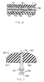
- Figure 3 illustrates a different prior art structure wherein the supports 28 and 29 of insulating support 30 are raised the desired spacing distance S above the conductive element 31.
- the spacing S will vary in an unacceptable manner due to the lack of a suitable holding force between belt 32 and supports 28 and 29 as well as other considerations.
- the present invention provides a spacing technique wherein a smooth, flexible dielectric surface is unsupported in the region of the electrodes or conductive element forming a part of an arcuate print head, the spacing being achieved by the formation of support surfaces that are interrupted in the region of the conductor together with careful construction of the flexible dielectric belt that provides the charge receiving surface.
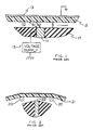
- Figure 4 illustrates a preferred form of the invention wherein a generally cylindrical support surface 40 is provided for the flexible dielectric belt 41, support surface 40 having an essentially flat region 42 provided in the region of and adjacent to the conductive element 44.
- Belt 41 is provided with a conductive coating member 43 and a reinforcing member 45 (of suitable material such as Mylar Plastic) and is suitably driven and very nearly conforms to the generally cylindrical support surfaces 46 and 47 (having common centers) except for the desired space S in the region of element 44.
- the spacing S is geometrically predictable and deviates from simple geometry when the belt 41 is under tension T as a function of that tension, the cylindrical radius and bending modulus of the belt.
- the tensioned belt which consists of elements 41, 45 and 43 is formed of a material that has a sufficiently high bending modulus to ensure formation of the desired gap S and to preclude substantial conformity of belt 41 in print head area 42 so as to permit the belt 41 and the electrode 44 to touch; by the same token, the bending modulus must be low enough to permit the needed belt deflection to generally follow the cylindrical surface 40 under tension forces. It is also believed quite important that belt shall have a smooth surface engaging the support surface 40 and that there are no abrupt surface discontinuities on print head support surface 40 to effect undue belt wear, accumulate foreign matter or to modify the desired spacing or electric characteristics. Clearly it is desirable to use materials for the belt and support surfaces to minimize unwanted static charging of the belt, which materials will also provide good release surface characteristics for avoiding unwanted accumulation of foreign matter which adversely affects the desired charging characteristics.
- FIG. 5 which describes apparatus substantially identical to FIG. 4, schematically discloses a frame 60, suitably supported, to which snubbers 62 and 63 are secured. Snubbers 62 and 63 are formed from a resilient material and provided with a low-friction felt nap coating 65 which engages the foil coating of belt 67; such a structure has been found to be an acceptable technique for controlling such waves so as to maintain the desired spacing S between electrode 68 and dielectric belt 67.
- FIGS. 6 and 7. One form of construction of the print head of this invention is shown in FIGS. 6 and 7.
- the assembly includes a pair of printed circuit boards 71 and 72, each board having an insulating substrate 74 supporting a plurality of individual conductive electrodes 76 as desired.
- the electrode pattern is such that the electrodes on board 71 are off-set from those on board 72.
- an insulating separator 78 is disposed between the boards (and conductors) with an epoxy cement 79 substantially filling any void or space.
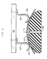
- FIG. 7 shows the dielectric member or belt 80 in dotted lines to show the cooperation with the print head generally designated 82, which print head is substantially as shown in the preceding FIG. 4.
- FIG. 7 is a cross-section view showing the electrode assembly of FIG. 6 sandwiched between and supported by two contoured belt support elements 84 and 85, which elements are configured as previously described to provide the desired belt spacing S from the ends of electrodes 76.
- Elements 84 and 85 are preferably formed of laminated fiberglass and epoxy to provide suitable strength and electrical insulation and are thereafter lapped and polished to provide the desired support radius and flattened area.
- a suitable connector 88 establishes electrical connection between the electrodes through cable 89 to drive circuit 90.
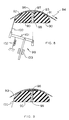
- FIG. 8 wherein the invention of FIG. 4 is partially illustrated but without electronics, conductive belt backing, etc., it is seen that cylindrical support 90 provides the desired cylindrical belt support surface 91 and 92 for dielectric belt 93, which belt is under tension and suitably driven in the direction of arrow 94. Tension forces, belt thickness, etc. are selected as before, with particular attention being given to the bending modulus so as to establish the desired belt/electrode gap 96.
- the region 97 in the area of the electrodes 98 is a discontinuity in cylindrical support 90 but that discontinuity can be of any desired configuration so long as belt support surfaces are smooth, the belt is smooth and the desired gap 96 is provided and maintained.
- the cleaning apparatus generally designated 99 is effectively utilized.
- a fairly flexible cleaning member 100 is mounted on pivoted arm 101, the arm being biased to a non-use position by spring 102 and movable by solenoid 103 to insert cleaning member 100 beneath moving belt 93 over support surface 92. Movement of the cleaning member 100 into the region of support area 92 thereafter to area 97 and support surface 91 is facilitated by movement of belt 93 which, in effect, drags the cleaning member along.
- cleaning member 100 is a soft, compressible fibrous material such as paper and its movement into the area to be cleaned is facilitated as best seen in FIG. 9, where like numbers are used for the like members and elements of FIG. 8.
- Fibrous paper cleaning element has a typical thickness of 2 to 3 mils (0.05 to 0.076 mm).
- Gap 96 (FIG.8) is preferably in the range of .25 mils (0.00635 mm).
- the soft fibrous material fills the gap area 96, (and may be compressed) to the point of actually deflecting belt 93 because of its thickness as it moves across the support surfaces.
Landscapes
- Physics & Mathematics (AREA)
- General Physics & Mathematics (AREA)
- Printers Or Recording Devices Using Electromagnetic And Radiation Means (AREA)
- Dot-Matrix Printers And Others (AREA)
- Electrophotography Using Other Than Carlson'S Method (AREA)
- Discharging, Photosensitive Material Shape In Electrophotography (AREA)
Applications Claiming Priority (2)
| Application Number | Priority Date | Filing Date | Title |
|---|---|---|---|
| US794640 | 1985-11-04 | ||
| US06/794,640 US4638339A (en) | 1985-11-04 | 1985-11-04 | Electrographic charge deposition apparatus |
Publications (3)
| Publication Number | Publication Date |
|---|---|
| EP0223481A2 EP0223481A2 (en) | 1987-05-27 |
| EP0223481A3 EP0223481A3 (en) | 1989-03-29 |
| EP0223481B1 true EP0223481B1 (en) | 1993-01-27 |
Family
ID=25163218
Family Applications (1)
| Application Number | Title | Priority Date | Filing Date |
|---|---|---|---|
| EP86308561A Expired - Lifetime EP0223481B1 (en) | 1985-11-04 | 1986-11-03 | Electrographic charge deposition apparatus |
Country Status (6)
| Country | Link |
|---|---|
| US (1) | US4638339A (Direct) |
| EP (1) | EP0223481B1 (Direct) |
| JP (1) | JPS62111763A (Direct) |
| KR (1) | KR870005275A (Direct) |
| CA (1) | CA1258087A (Direct) |
| DE (1) | DE3687624T2 (Direct) |
Families Citing this family (8)
| Publication number | Priority date | Publication date | Assignee | Title |
|---|---|---|---|---|
| US4831393A (en) * | 1987-12-11 | 1989-05-16 | Moore Business Forms, Inc. | Belt and belt support for non-impact, direct charge electrographic printer |
| US4823153A (en) * | 1987-12-11 | 1989-04-18 | Moore Business Forms, Inc. | Cleaning system for non-impact printer |
| US4839673A (en) * | 1987-12-11 | 1989-06-13 | Moore Business Forms, Inc. | AC corona enhancement for electrostatic imaging devices |
| US4827295A (en) * | 1987-12-11 | 1989-05-02 | Moore Business Forms, Inc. | Conditioning apparatus for non-impact, direct charge electrographic printer belt |
| US4862198A (en) * | 1988-10-06 | 1989-08-29 | Moore Business Forms, Inc. | Electrostatic cleaning of electrodes in an electrographic printer |
| US5107283A (en) * | 1989-12-27 | 1992-04-21 | Nippon Steel Corporation | Electrostatic recording head with improved alignment of recording electrodes |
| JPH0946494A (ja) * | 1995-05-24 | 1997-02-14 | Ricoh Co Ltd | 画像形成装置 |
| US6028614A (en) * | 1997-11-13 | 2000-02-22 | Clark; Lloyd Douglas | Cleaning and lapping apparatus and method for electrographic printers |
Family Cites Families (7)
| Publication number | Priority date | Publication date | Assignee | Title |
|---|---|---|---|---|
| DE2125302A1 (de) * | 1971-05-21 | 1972-11-30 | Philips Patentverwaltung | Vorrichtung zur Ladungsbilderzeugung bei der elektrostatischen Elektrographie |
| US4227452A (en) * | 1977-10-14 | 1980-10-14 | Fuji Xerox Co., Ltd. | Printing machine |
| US4218641A (en) * | 1978-11-16 | 1980-08-19 | International Business Machines Corporation | Analog DC motor velocity control loop |
| JPS5687057A (en) * | 1979-12-18 | 1981-07-15 | Fuji Xerox Co Ltd | Electrostatic recording electrode head |
| JPS57179879A (en) * | 1981-04-30 | 1982-11-05 | Fujitsu Ltd | Recorder |
| DE3170780D1 (en) * | 1980-12-24 | 1985-07-04 | Fujitsu Ltd | Direct imaging method and electrostatic printing equipment |
| US4527177A (en) * | 1983-08-29 | 1985-07-02 | Xerox Corporation | Ion projection printer with virtual back electrode |
-
1985
- 1985-11-04 US US06/794,640 patent/US4638339A/en not_active Expired - Fee Related
-
1986
- 1986-10-23 CA CA000521208A patent/CA1258087A/en not_active Expired
- 1986-10-30 JP JP61257128A patent/JPS62111763A/ja active Granted
- 1986-11-03 EP EP86308561A patent/EP0223481B1/en not_active Expired - Lifetime
- 1986-11-03 DE DE8686308561T patent/DE3687624T2/de not_active Expired - Fee Related
- 1986-11-04 KR KR860009280A patent/KR870005275A/ko not_active Withdrawn
Also Published As
| Publication number | Publication date |
|---|---|
| JPS62111763A (ja) | 1987-05-22 |
| US4638339A (en) | 1987-01-20 |
| EP0223481A3 (en) | 1989-03-29 |
| JPH0476311B2 (Direct) | 1992-12-03 |
| EP0223481A2 (en) | 1987-05-27 |
| DE3687624D1 (de) | 1993-03-11 |
| KR870005275A (ko) | 1987-06-05 |
| DE3687624T2 (de) | 1993-09-02 |
| CA1258087A (en) | 1989-08-01 |
Similar Documents
| Publication | Publication Date | Title |
|---|---|---|
| US5121170A (en) | Device for transporting sheet members using an alternating voltage | |
| EP0435549B1 (en) | Apertured printhead for direct electrostatic printing | |
| EP0376669B1 (en) | Electrostatic printing apparatus | |
| EP0352997B1 (en) | Direct electrostatic printer (DEP) and printhead structure therefor | |
| EP0720072B1 (en) | Image forming apparatus | |
| EP0345024B1 (en) | Printing apparatus and toner/developer delivery system therefor | |
| JPH07242013A (ja) | 画像形成装置 | |
| EP0223481B1 (en) | Electrographic charge deposition apparatus | |
| US5821972A (en) | Electrographic printing apparatus and method | |
| JPH03196061A (ja) | 直接式静電印刷のためのベルトドナー | |
| US6314265B1 (en) | Transfer printing station for an electrographic device with a contact pressure element in the transfer printing area | |
| JPH07304206A (ja) | 画像形成装置 | |
| JPH06336047A (ja) | 画像形成装置 | |
| JP3402890B2 (ja) | 画像形成装置 | |
| US5867190A (en) | Image forming unit with control electrodes arranged to be electrically insulated from each other | |
| US4862198A (en) | Electrostatic cleaning of electrodes in an electrographic printer | |
| US6336712B1 (en) | Image formation apparatus having a toner flow control member with a protection layer | |
| JP2000355115A (ja) | 画像形成装置 | |
| JP3127516B2 (ja) | 画像記録装置 | |
| JPH06344588A (ja) | 画像形成装置 | |
| JP3055191B2 (ja) | 画像形成装置 | |
| JPH0858146A (ja) | 画像形成装置 | |
| EP0631208A2 (en) | Method and apparatus for forming an image on a recording medium | |
| JPH0761025A (ja) | 画像形成装置 | |
| JPH0880633A (ja) | 画像形成装置 |
Legal Events
| Date | Code | Title | Description |
|---|---|---|---|
| PUAI | Public reference made under article 153(3) epc to a published international application that has entered the european phase |
Free format text: ORIGINAL CODE: 0009012 |
|
| AK | Designated contracting states |
Kind code of ref document: A2 Designated state(s): DE FR GB IT |
|
| PUAL | Search report despatched |
Free format text: ORIGINAL CODE: 0009013 |
|
| AK | Designated contracting states |
Kind code of ref document: A3 Designated state(s): DE FR GB IT |
|
| 17P | Request for examination filed |
Effective date: 19890822 |
|
| 17Q | First examination report despatched |
Effective date: 19910328 |
|
| RAP1 | Party data changed (applicant data changed or rights of an application transferred) |
Owner name: MOORE BUSINESS FORMS, INC. |
|
| GRAA | (expected) grant |
Free format text: ORIGINAL CODE: 0009210 |
|
| AK | Designated contracting states |
Kind code of ref document: B1 Designated state(s): DE FR GB IT |
|
| PG25 | Lapsed in a contracting state [announced via postgrant information from national office to epo] |
Ref country code: IT Free format text: LAPSE BECAUSE OF FAILURE TO SUBMIT A TRANSLATION OF THE DESCRIPTION OR TO PAY THE FEE WITHIN THE PRESCRIBED TIME-LIMIT;WARNING: LAPSES OF ITALIAN PATENTS WITH EFFECTIVE DATE BEFORE 2007 MAY HAVE OCCURRED AT ANY TIME BEFORE 2007. THE CORRECT EFFECTIVE DATE MAY BE DIFFERENT FROM THE ONE RECORDED. Effective date: 19930127 |
|
| ET | Fr: translation filed | ||
| REF | Corresponds to: |
Ref document number: 3687624 Country of ref document: DE Date of ref document: 19930311 |
|
| PLBE | No opposition filed within time limit |
Free format text: ORIGINAL CODE: 0009261 |
|
| STAA | Information on the status of an ep patent application or granted ep patent |
Free format text: STATUS: NO OPPOSITION FILED WITHIN TIME LIMIT |
|
| 26N | No opposition filed | ||
| GBPC | Gb: european patent ceased through non-payment of renewal fee |
Effective date: 19931103 |
|
| REG | Reference to a national code |
Ref country code: GB Ref legal event code: 728V |
|
| REG | Reference to a national code |
Ref country code: GB Ref legal event code: 732E |
|
| REG | Reference to a national code |
Ref country code: GB Ref legal event code: 728Y |
|
| PGFP | Annual fee paid to national office [announced via postgrant information from national office to epo] |
Ref country code: GB Payment date: 19961031 Year of fee payment: 11 |
|
| PGFP | Annual fee paid to national office [announced via postgrant information from national office to epo] |
Ref country code: DE Payment date: 19961108 Year of fee payment: 11 |
|
| PGFP | Annual fee paid to national office [announced via postgrant information from national office to epo] |
Ref country code: FR Payment date: 19961111 Year of fee payment: 11 |
|
| PG25 | Lapsed in a contracting state [announced via postgrant information from national office to epo] |
Ref country code: GB Free format text: LAPSE BECAUSE OF NON-PAYMENT OF DUE FEES Effective date: 19971103 |
|
| PG25 | Lapsed in a contracting state [announced via postgrant information from national office to epo] |
Ref country code: FR Free format text: THE PATENT HAS BEEN ANNULLED BY A DECISION OF A NATIONAL AUTHORITY Effective date: 19971130 |
|
| GBPC | Gb: european patent ceased through non-payment of renewal fee |
Effective date: 19971103 |
|
| PG25 | Lapsed in a contracting state [announced via postgrant information from national office to epo] |
Ref country code: DE Free format text: LAPSE BECAUSE OF NON-PAYMENT OF DUE FEES Effective date: 19980801 |
|
| REG | Reference to a national code |
Ref country code: FR Ref legal event code: ST |