EP0221666A2 - Systeme zur Darstellung von Hartkopien und zur Speicherung von Signalen - Google Patents
Systeme zur Darstellung von Hartkopien und zur Speicherung von Signalen Download PDFInfo
- Publication number
- EP0221666A2 EP0221666A2 EP86307452A EP86307452A EP0221666A2 EP 0221666 A2 EP0221666 A2 EP 0221666A2 EP 86307452 A EP86307452 A EP 86307452A EP 86307452 A EP86307452 A EP 86307452A EP 0221666 A2 EP0221666 A2 EP 0221666A2
- Authority
- EP
- European Patent Office
- Prior art keywords
- signal
- channel
- circuit
- regulation
- memory
- Prior art date
- Legal status (The legal status is an assumption and is not a legal conclusion. Google has not performed a legal analysis and makes no representation as to the accuracy of the status listed.)
- Ceased
Links
Images
Classifications
-
- G—PHYSICS
- G06—COMPUTING OR CALCULATING; COUNTING
- G06K—GRAPHICAL DATA READING; PRESENTATION OF DATA; RECORD CARRIERS; HANDLING RECORD CARRIERS
- G06K15/00—Arrangements for producing a permanent visual presentation of the output data, e.g. computer output printers
-
- G—PHYSICS
- G06—COMPUTING OR CALCULATING; COUNTING
- G06F—ELECTRIC DIGITAL DATA PROCESSING
- G06F3/00—Input arrangements for transferring data to be processed into a form capable of being handled by the computer; Output arrangements for transferring data from processing unit to output unit, e.g. interface arrangements
- G06F3/14—Digital output to display device ; Cooperation and interconnection of the display device with other functional units
- G06F3/153—Digital output to display device ; Cooperation and interconnection of the display device with other functional units using cathode-ray tubes
-
- G—PHYSICS
- G06—COMPUTING OR CALCULATING; COUNTING
- G06K—GRAPHICAL DATA READING; PRESENTATION OF DATA; RECORD CARRIERS; HANDLING RECORD CARRIERS
- G06K2215/00—Arrangements for producing a permanent visual presentation of the output data
- G06K2215/0082—Architecture adapted for a particular function
- G06K2215/0091—Outputting only video data, e.g. Hard copy of CRT display
Definitions
- This invention relates to hard copy and signal storage systems and is primarily concerned with so regulating the non-uniformity of video and other signals from a plurality of graphic terminals providing RGB (red, green and blue) video or like signals so as to obtain correct hard copies and/or correct stored signals when signals from these terminals are switched by a multiplexer device whose output is used to make the required copies and/or is otherwise stored.
- the principal object of the invention is to enable the multiplexer device used in the system to be one which does not have to include means of regulation and therefore to be of simple construction and low cost. As will be seen later this object is achieved by making the multiplexer device have channel discrimination signals and by providing means, based on said channel discrimination signals, for controlling a signal take-in element.
- RGB video signals When RGB video signals are taken in, it is often found that they have differences in amplitude and phase generally, even when they are to the same specification. If no regulation of amplitude and phase is applied, data take-in errors occur and these produce incorrect hard copies or stored signals when the unregulated signals are used to make hard copies or are stored. Accordingly, when a plurality of graphic terminals are connected with the same hard copy system (for example),regulation circuits are provided for regulation of the signals supplied from the plurality of graphic terminals in the system.
- the said multiplexer device In previously known systems in which signals from a number of graphic terminals are fed in to a multiplexer device, the said multiplexer device has had to be one providing regulation in a plurality of channels and this involves that the said device must be of complicated circuit construction and therefore expensive.
- a further disadvantage of the said previously known systems is that the multiplexer device cannot be connected to graphic terminals of different kinds and which are different in specification e.g. if one or more is of video frequency and another is of a horizontal frequency.
- the present invention seeks to avoid the above disadvantages and to provide a hard copy or signal storage system in which a multiplexer device connected to a plurality of graphic terminals - even if these are of different kinds -can be of simple and inexpensive construction, for example composed mainly of switching means using relays or the like because it is not required to effect signal amplitude or phase regulation in the different channels.
- a signal storage system in which a plurality of selectable graphic terminals are connectable through a multiplexer device to signal utilisation means is characterised in that the multiplexer device includes channel switching means and a channel discrimination signal output circuit, and the signal utilisation means include a channel discrimination recognition circuit fed from the signal output circuit, a signal take-in element fed from the switching means, a signal storage circuit supplied with signals from the element, a memory in which regulation and specification values appropriate to said graphic terminals are stored, and a central processing unit providing correct regulation by controlling the element in accordance with information stored in the memory, whereby the need for regulation in the multiplexer device is avoided.
- a channel discrimination signal output circuit in the multiplexer device in the multiplexer device; a channel discrimination signal recognition circuit; and video signal take-in means controllable as to regulation value and specification value by a central processing unit (CPU) and (in the hard copy system) a non-volatile Random Access Memory (RAM) capable of storing and rewriting the regulation values and specification values of the plurality of channels leading from the graphic terminals.
- CPU central processing unit
- RAM non-volatile Random Access Memory
- the specification of the video signals of each graphic terminal, and the regulation values enabling the optimum taking-in of video signals to be achieved are, when the apparatus is set up for use, stored as parameters in the non-voltatile RAM of the hard copy system.
- video signals from the graphic terminal thus selected are fed in to the hard copy system, and simultaneously a channel discrimination signal is delivered from the multiplexer device.
- the hard copy system reads the aforesaid previously set parameters out of the region of said channel in the non-volatile RAM, and delivers the same to the video signal take-in element. In this way, take-in of the video signals is automatically adjusted for optimum results. The operation of taking in the video signals is then started, and correct picture information is stored in the picture storage circuit of the hard copy system.
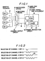
- GR1, GR2, GR3 and GR4 are four graphic terminals which are connected to a hard copy system generally designated 17 through the intermediary of a multiplexer device generally designated 13. Each graphic terminal feeds video signals to that multiplexer device through its output lead.
- the four output leads are referenced 12 in Figure 1.
- the multiplexer device 13 comprises a video signal switching means 14 and a channel discrimination signal output element 15.
- the video signal switching means 14 may be of quite simple construction; for example it may be composed of relays, and has four channels corresponding respectively to the four terminals GR1 to GR4. When a channel is selected, the appropriate relay switches in that channel i.e. closes it, and video signals are delivered unchanged to the hard copy system.
- the hard copy system 17 comprises a video signal take-in element 18, a channel discrimination signal recognition circuit 20, non-volatile RAM 22 capable of storing specifications and regulation values of video signals on the four channels, a picture storage circuit (GM) 19 and a CPU 21.
- GM picture storage circuit
- the hard copy system 17 determines by means of the channel discrimination signal recognition circuit 20 the channel along which an input video signal comes. The parameters of this channel are then read out of the memory 22 and fed out to the video signal take-in element 18. An operation of take-in of video signals is then started, and these signals are transmitted to the picture storage circuit 19 which stores as a picture video signals converted into digital signals under the control of the CPU 21.
- Figure 2 is a time chart of the channel discrimination signals prepared by the channel discrimination signal output circuit 15.
- these channel discrimination signals from circuit 15 are negative-going logic pulses corresponding to terminals GR1 to GR4.
- the circuit 15 may take any of a variety of forms well known per se - e.g. it may comprise bit switches with counters - and needs no detailed description here.
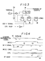
- FIG. 3 is a circuit diagram showing a suitable form which may be adopted for the channel discrimination signal recognition circuit 20 of Figure 1.
- a flip-flop circuit 34 detects the trailing edge of the channel discrimination signal,and 35 and 36 are further flip-flop circuits each of which latches the Q output of flip-flop 34 by a vertical sycnhronizing signal 32, herein termed the V signal.
- 33 is a counter which counts the number of pulses.
- a signal 37 herein termed the BUSY signal, is fed in as a "clear" signal to the counter, and the outputs (QA to QD) of the counter are connected to an input port CPU.
- Figure 4 is a timing chart showing the sequence of recognition of channels.
- the channel discrimination signal turns active (LOW) as at 42, the Q output signal from 34 becomes HIGH.
- the V signal the Q output from 35 becomes HIGH and, at the leading edge of a subsequent V signal at 44, the Q output from 36 becomes HIGH.
- This signal is fed to an input port of CPU which accordingly recognizes thereby that an external demand for copy has occurred.
- CPU reads out the values of the outputs QA to QD of counter 33 during a time period indicated by the shaded portion 41 of the line referenced CPU in Figure 4 and thus identifies which of the channels has been switched in by the multiplexer 13 of Figure 1.
- the outputs QA to QD of counter 33 show values which are counted up by the channel discrimination signal.
- the count values can be read exactly by a process of latching twice at the leading edge of the aforesaid V signal, provided, of course that the pulses for discriminating the channel come to an end within the time (46 in Figure 4) of one period of the V signal.
- CPU reads out parameters from the region of a selected channel in the RAM 22 ( Figure 1) and delivers the same to the video signal take-in element 18 ( Figure 1). It also makes the BUSY signal 37 become HIGH as at 45 for the counter 33 and the flip-flops 34, 35 and 36. Accordingly the channel discrimination signal becomes LOW as at 47 thus in effect informing the multiplexer device 13 that the hard copy system is in the course of taking in video signals and printing.
- the channel discrimination signals a conventional signal line for copy start and BUSY signals is used unchanged, and this line fulfills copy start and BUSY functions as well in the present system.
- the multiplexer device 13 does not need to have any regulation circuits and thus may be of simple construction even although there are a number of graphic terminals from which signals have to be taken. Because of this the cost of the apparatus can be made very substantially less than that of comparable known equipment.
- the invention is not limited to its use in connection with video signals of the same specification, but may be used to enable the connection of graphic terminals of different kinds to the same hard copy system.
- the invention is applicable not only to hard copy systems, but is generally applicable to systems of the kind in which video signals are stored graphically.
Landscapes
- Engineering & Computer Science (AREA)
- Theoretical Computer Science (AREA)
- General Engineering & Computer Science (AREA)
- Physics & Mathematics (AREA)
- General Physics & Mathematics (AREA)
- Human Computer Interaction (AREA)
- Television Signal Processing For Recording (AREA)
- Controls And Circuits For Display Device (AREA)
- Studio Circuits (AREA)
Applications Claiming Priority (2)
| Application Number | Priority Date | Filing Date | Title |
|---|---|---|---|
| JP218231/85 | 1985-10-01 | ||
| JP60218231A JPS6277636A (ja) | 1985-10-01 | 1985-10-01 | チヤンネル識別信号により制御できるハ−ドコピ−装置 |
Publications (2)
| Publication Number | Publication Date |
|---|---|
| EP0221666A2 true EP0221666A2 (de) | 1987-05-13 |
| EP0221666A3 EP0221666A3 (de) | 1990-03-28 |
Family
ID=16716661
Family Applications (1)
| Application Number | Title | Priority Date | Filing Date |
|---|---|---|---|
| EP86307452A Ceased EP0221666A3 (de) | 1985-10-01 | 1986-09-29 | Systeme zur Darstellung von Hartkopien und zur Speicherung von Signalen |
Country Status (3)
| Country | Link |
|---|---|
| US (1) | US4779140A (de) |
| EP (1) | EP0221666A3 (de) |
| JP (1) | JPS6277636A (de) |
Cited By (1)
| Publication number | Priority date | Publication date | Assignee | Title |
|---|---|---|---|---|
| EP0497599A3 (en) * | 1991-02-01 | 1993-03-24 | Canon Kabushiki Kaisha | Image processing apparatus |
Family Cites Families (3)
| Publication number | Priority date | Publication date | Assignee | Title |
|---|---|---|---|---|
| US4034400A (en) * | 1970-09-23 | 1977-07-05 | International Publishing Corporation Ltd. | Apparatus for reproducing graphic material |
| US4228466A (en) * | 1978-03-13 | 1980-10-14 | Exxon Research & Engineering Co. | Transmission mode signaling between a facsimile transmitter and a facsimile receiver |
| US4558369A (en) * | 1982-12-28 | 1985-12-10 | Iwasaki Tsushinki Kabushiki Kaisha | Facsimile connection system |
-
1985
- 1985-10-01 JP JP60218231A patent/JPS6277636A/ja active Pending
-
1986
- 1986-09-29 EP EP86307452A patent/EP0221666A3/de not_active Ceased
- 1986-09-30 US US06/913,685 patent/US4779140A/en not_active Expired - Fee Related
Non-Patent Citations (1)
| Title |
|---|
| IBM TECHNICAL DISCLOSURE BULLETIN, vol. 26, no. 10B, March 1984, pages 5336-5339, New York, NY, US; R.T. HEATH et al.: "Method for achieving display/printer independence on a shared printer" * |
Cited By (2)
| Publication number | Priority date | Publication date | Assignee | Title |
|---|---|---|---|---|
| EP0497599A3 (en) * | 1991-02-01 | 1993-03-24 | Canon Kabushiki Kaisha | Image processing apparatus |
| US5499362A (en) * | 1991-02-01 | 1996-03-12 | Canon Kabushiki Kaisha | Image processing apparatus |
Also Published As
| Publication number | Publication date |
|---|---|
| US4779140A (en) | 1988-10-18 |
| JPS6277636A (ja) | 1987-04-09 |
| EP0221666A3 (de) | 1990-03-28 |
Similar Documents
| Publication | Publication Date | Title |
|---|---|---|
| EP0386935A2 (de) | Gerät, das fähig ist, die Anzahl von Wartezuständen für den Zugriff zu variieren | |
| US4658349A (en) | Direct memory access control circuit and data processing system using said circuit | |
| US3806826A (en) | Digital circuit for adjusting the frequency of a variable frequency oscillator | |
| US5019907A (en) | Pulse generating circuit | |
| US3573744A (en) | Data buffer system for transferring information from a first to a second storage medium | |
| DE69124606T2 (de) | Adaptive FIFO-Speichersteuerung | |
| EP0205544B1 (de) | Frequenzenverteiler | |
| JPH01309589A (ja) | ビデオ信号処理用制御信号発生器 | |
| US4071889A (en) | Central processing apparatus for generating and receiving time division multiplex signals | |
| US4779140A (en) | Hard copy system controllable by channel discrimination signal | |
| US4012589A (en) | Switching arrangement for transmitting data in time division multiplex systems | |
| US4942478A (en) | Recording apparatus | |
| US4434420A (en) | Interline spacing adjustment circuit in a scanning CRT visual display system | |
| US4310855A (en) | Efficient multichannel automatic setup and remote control system | |
| EP0651585B1 (de) | Steuerschaltung für analoge Schaltungen mit anzeigenden Signalen für die Kontrollspannungen und deren Art | |
| DE68922282T2 (de) | Bildlesesystem. | |
| US5144650A (en) | Communication apparatus having improved switching line connection between different signal paths | |
| JP2752082B2 (ja) | デジタル信号処理回路の制御装置 | |
| DE69326396T2 (de) | Verfahren und Vorrichtung zum Verarbeiten in der Verbindung abwärtsgerichteter digitaler Stimmendaten | |
| JPS6218110B2 (de) | ||
| US3551651A (en) | Arrangement for digitally establishing a value | |
| CA1058764A (en) | Serial data reception system | |
| US6052075A (en) | Data processing device having a D/A function | |
| KR960007565B1 (ko) | 헤더처리순서신호 자동발생장치 | |
| JPS5995733A (ja) | フエイズロツクドル−プ用集積回路キツト |
Legal Events
| Date | Code | Title | Description |
|---|---|---|---|
| PUAI | Public reference made under article 153(3) epc to a published international application that has entered the european phase |
Free format text: ORIGINAL CODE: 0009012 |
|
| AK | Designated contracting states |
Kind code of ref document: A2 Designated state(s): DE FR GB |
|
| RAP1 | Party data changed (applicant data changed or rights of an application transferred) |
Owner name: SEIKO INSTRUMENTS INC. |
|
| PUAL | Search report despatched |
Free format text: ORIGINAL CODE: 0009013 |
|
| AK | Designated contracting states |
Kind code of ref document: A3 Designated state(s): DE FR GB |
|
| 17P | Request for examination filed |
Effective date: 19900604 |
|
| 17Q | First examination report despatched |
Effective date: 19911030 |
|
| STAA | Information on the status of an ep patent application or granted ep patent |
Free format text: STATUS: THE APPLICATION HAS BEEN REFUSED |
|
| 18R | Application refused |
Effective date: 19920310 |
|
| RIN1 | Information on inventor provided before grant (corrected) |
Inventor name: WATANABE, SHINYASEIKO INSTRUMENT & Inventor name: YAMAGUCHI, KANEOSEIKO INSTRUMENT & Inventor name: MATSUSHIMA, KENICHISEIKO INSTRUMENT & Inventor name: TANAKA, FUMIHIROSEIKO INSTRUMENT & Inventor name: SHIMADA, YOSHIOSEIKO INSTRUMENT & |