EP0221496A2 - Empaquetage pour circuit intégré - Google Patents
Empaquetage pour circuit intégré Download PDFInfo
- Publication number
- EP0221496A2 EP0221496A2 EP86114966A EP86114966A EP0221496A2 EP 0221496 A2 EP0221496 A2 EP 0221496A2 EP 86114966 A EP86114966 A EP 86114966A EP 86114966 A EP86114966 A EP 86114966A EP 0221496 A2 EP0221496 A2 EP 0221496A2
- Authority
- EP
- European Patent Office
- Prior art keywords
- integrated circuit
- package
- chip
- lead frame
- chips
- Prior art date
- Legal status (The legal status is an assumption and is not a legal conclusion. Google has not performed a legal analysis and makes no representation as to the accuracy of the status listed.)
- Withdrawn
Links
Images
Classifications
-
- H—ELECTRICITY
- H01—ELECTRIC ELEMENTS
- H01L—SEMICONDUCTOR DEVICES NOT COVERED BY CLASS H10
- H01L23/00—Details of semiconductor or other solid state devices
- H01L23/48—Arrangements for conducting electric current to or from the solid state body in operation, e.g. leads, terminal arrangements ; Selection of materials therefor
- H01L23/488—Arrangements for conducting electric current to or from the solid state body in operation, e.g. leads, terminal arrangements ; Selection of materials therefor consisting of soldered or bonded constructions
- H01L23/495—Lead-frames or other flat leads
- H01L23/49575—Assemblies of semiconductor devices on lead frames
-
- H—ELECTRICITY
- H01—ELECTRIC ELEMENTS
- H01L—SEMICONDUCTOR DEVICES NOT COVERED BY CLASS H10
- H01L2224/00—Indexing scheme for arrangements for connecting or disconnecting semiconductor or solid-state bodies and methods related thereto as covered by H01L24/00
- H01L2224/01—Means for bonding being attached to, or being formed on, the surface to be connected, e.g. chip-to-package, die-attach, "first-level" interconnects; Manufacturing methods related thereto
- H01L2224/02—Bonding areas; Manufacturing methods related thereto
- H01L2224/04—Structure, shape, material or disposition of the bonding areas prior to the connecting process
- H01L2224/05—Structure, shape, material or disposition of the bonding areas prior to the connecting process of an individual bonding area
- H01L2224/0554—External layer
- H01L2224/0555—Shape
- H01L2224/05552—Shape in top view
- H01L2224/05553—Shape in top view being rectangular
-
- H—ELECTRICITY
- H01—ELECTRIC ELEMENTS
- H01L—SEMICONDUCTOR DEVICES NOT COVERED BY CLASS H10
- H01L2224/00—Indexing scheme for arrangements for connecting or disconnecting semiconductor or solid-state bodies and methods related thereto as covered by H01L24/00
- H01L2224/01—Means for bonding being attached to, or being formed on, the surface to be connected, e.g. chip-to-package, die-attach, "first-level" interconnects; Manufacturing methods related thereto
- H01L2224/42—Wire connectors; Manufacturing methods related thereto
- H01L2224/47—Structure, shape, material or disposition of the wire connectors after the connecting process
- H01L2224/48—Structure, shape, material or disposition of the wire connectors after the connecting process of an individual wire connector
- H01L2224/4805—Shape
- H01L2224/4809—Loop shape
- H01L2224/48091—Arched
-
- H—ELECTRICITY
- H01—ELECTRIC ELEMENTS
- H01L—SEMICONDUCTOR DEVICES NOT COVERED BY CLASS H10
- H01L2224/00—Indexing scheme for arrangements for connecting or disconnecting semiconductor or solid-state bodies and methods related thereto as covered by H01L24/00
- H01L2224/01—Means for bonding being attached to, or being formed on, the surface to be connected, e.g. chip-to-package, die-attach, "first-level" interconnects; Manufacturing methods related thereto
- H01L2224/42—Wire connectors; Manufacturing methods related thereto
- H01L2224/47—Structure, shape, material or disposition of the wire connectors after the connecting process
- H01L2224/48—Structure, shape, material or disposition of the wire connectors after the connecting process of an individual wire connector
- H01L2224/481—Disposition
- H01L2224/48151—Connecting between a semiconductor or solid-state body and an item not being a semiconductor or solid-state body, e.g. chip-to-substrate, chip-to-passive
- H01L2224/48221—Connecting between a semiconductor or solid-state body and an item not being a semiconductor or solid-state body, e.g. chip-to-substrate, chip-to-passive the body and the item being stacked
- H01L2224/48245—Connecting between a semiconductor or solid-state body and an item not being a semiconductor or solid-state body, e.g. chip-to-substrate, chip-to-passive the body and the item being stacked the item being metallic
- H01L2224/48247—Connecting between a semiconductor or solid-state body and an item not being a semiconductor or solid-state body, e.g. chip-to-substrate, chip-to-passive the body and the item being stacked the item being metallic connecting the wire to a bond pad of the item
-
- H—ELECTRICITY
- H01—ELECTRIC ELEMENTS
- H01L—SEMICONDUCTOR DEVICES NOT COVERED BY CLASS H10
- H01L2224/00—Indexing scheme for arrangements for connecting or disconnecting semiconductor or solid-state bodies and methods related thereto as covered by H01L24/00
- H01L2224/01—Means for bonding being attached to, or being formed on, the surface to be connected, e.g. chip-to-package, die-attach, "first-level" interconnects; Manufacturing methods related thereto
- H01L2224/42—Wire connectors; Manufacturing methods related thereto
- H01L2224/47—Structure, shape, material or disposition of the wire connectors after the connecting process
- H01L2224/49—Structure, shape, material or disposition of the wire connectors after the connecting process of a plurality of wire connectors
- H01L2224/491—Disposition
- H01L2224/4912—Layout
- H01L2224/49171—Fan-out arrangements
-
- H—ELECTRICITY
- H01—ELECTRIC ELEMENTS
- H01L—SEMICONDUCTOR DEVICES NOT COVERED BY CLASS H10
- H01L24/00—Arrangements for connecting or disconnecting semiconductor or solid-state bodies; Methods or apparatus related thereto
- H01L24/01—Means for bonding being attached to, or being formed on, the surface to be connected, e.g. chip-to-package, die-attach, "first-level" interconnects; Manufacturing methods related thereto
- H01L24/42—Wire connectors; Manufacturing methods related thereto
- H01L24/47—Structure, shape, material or disposition of the wire connectors after the connecting process
- H01L24/48—Structure, shape, material or disposition of the wire connectors after the connecting process of an individual wire connector
-
- H—ELECTRICITY
- H01—ELECTRIC ELEMENTS
- H01L—SEMICONDUCTOR DEVICES NOT COVERED BY CLASS H10
- H01L24/00—Arrangements for connecting or disconnecting semiconductor or solid-state bodies; Methods or apparatus related thereto
- H01L24/01—Means for bonding being attached to, or being formed on, the surface to be connected, e.g. chip-to-package, die-attach, "first-level" interconnects; Manufacturing methods related thereto
- H01L24/42—Wire connectors; Manufacturing methods related thereto
- H01L24/47—Structure, shape, material or disposition of the wire connectors after the connecting process
- H01L24/49—Structure, shape, material or disposition of the wire connectors after the connecting process of a plurality of wire connectors
-
- H—ELECTRICITY
- H01—ELECTRIC ELEMENTS
- H01L—SEMICONDUCTOR DEVICES NOT COVERED BY CLASS H10
- H01L2924/00—Indexing scheme for arrangements or methods for connecting or disconnecting semiconductor or solid-state bodies as covered by H01L24/00
- H01L2924/0001—Technical content checked by a classifier
- H01L2924/00014—Technical content checked by a classifier the subject-matter covered by the group, the symbol of which is combined with the symbol of this group, being disclosed without further technical details
-
- H—ELECTRICITY
- H01—ELECTRIC ELEMENTS
- H01L—SEMICONDUCTOR DEVICES NOT COVERED BY CLASS H10
- H01L2924/00—Indexing scheme for arrangements or methods for connecting or disconnecting semiconductor or solid-state bodies as covered by H01L24/00
- H01L2924/01—Chemical elements
- H01L2924/01079—Gold [Au]
-
- H—ELECTRICITY
- H01—ELECTRIC ELEMENTS
- H01L—SEMICONDUCTOR DEVICES NOT COVERED BY CLASS H10
- H01L2924/00—Indexing scheme for arrangements or methods for connecting or disconnecting semiconductor or solid-state bodies as covered by H01L24/00
- H01L2924/10—Details of semiconductor or other solid state devices to be connected
- H01L2924/1015—Shape
- H01L2924/1016—Shape being a cuboid
- H01L2924/10161—Shape being a cuboid with a rectangular active surface
-
- H—ELECTRICITY
- H01—ELECTRIC ELEMENTS
- H01L—SEMICONDUCTOR DEVICES NOT COVERED BY CLASS H10
- H01L2924/00—Indexing scheme for arrangements or methods for connecting or disconnecting semiconductor or solid-state bodies as covered by H01L24/00
- H01L2924/10—Details of semiconductor or other solid state devices to be connected
- H01L2924/11—Device type
- H01L2924/14—Integrated circuits
-
- H—ELECTRICITY
- H01—ELECTRIC ELEMENTS
- H01L—SEMICONDUCTOR DEVICES NOT COVERED BY CLASS H10
- H01L2924/00—Indexing scheme for arrangements or methods for connecting or disconnecting semiconductor or solid-state bodies as covered by H01L24/00
- H01L2924/15—Details of package parts other than the semiconductor or other solid state devices to be connected
- H01L2924/181—Encapsulation
Definitions
- This invention relates to integrated circuit packages including integrated circuit chips.
- the dual inline pin integrated circuit package known in the industry as the DIP package, is found in most data processing systems.
- US-A-4,398,235 shows an arrangement whereby a plurality of these integrated circuits is stacked in a piggyback fashion with the appropriate pins electrically connected together and other pins cut off. This approach is particularly useful in increasing random access and read only memory density.
- the space requirements for the increased height of the printed circuit card on which these devices are piggybacked must be greater than for a card populated with non-piggybacked modules, but the area requirements for the card do not increase.
- US-A-3,746,934 discloses a stacked arrangement of integrated circuit chips which includes a stack of frames, each formed with connecting leads and known as a lead frame, with integrated circuit chips mounted on one side only of each lead frame.
- the lead frames are then electrically interconnected and the entire arrangement may then be appropriately encapsulated. Since there must be separation between the plurality of lead frames in this package, like the piggyback arrangement described above, this package has a height dimension which is nearly equal to its multiple of circuit density.
- US-A-4,423,468 shows a package in which associated miniature electronic components, such as a bare micro processor and its associated unpackaged read only memory chip, are mounted on opposite sides of an insulating substrate which, in effect, amounts to a miniature, double sided printed circuit card. Wire bonding connects the contact points on the semiconductor chips to conductive patterns on the insulating substrate. The insulating substrate is then sealed by insulating covers on each side of the substrate and the entire assembly may be reflow soldered to external circuitry as a surface mounted component module. While this technique is yet another approach to increasing the density of mounted integrated circuit chips, it is a rather complex arrangement which is equivalent to a double sided printed circuit card having bare chips mounted thereon and being further enclosed in a protective case. Although such an approach does yield higher circuit densities, its complexity leads to substantially higher costs.
- the object of the present invention is to provide an improved integrated circuit package.
- the present invention relates to an integrated circuit package of the type which comprises a lead frame formed with a plurality of connecting leads and two substantially identical integrated circuit chips mounted on the lead frame.
- An integrated circuit package in accordance with the invention is characterised in that one integrated circuit chip is mounted on one side of the frame, the other integrated circuit chip is mounted on the other side of the frame, and each pair of corresponding terminals of the two integrated circuit chips are connected to the same connecting lead of the frame.
- the double integrated circuit chip package according to the invention is slightly thicker than a conventional module which allows integrated circuit chips to be mounted on only one side of the lead frame.
- a packaging arrangement according to the invention yields a package substantially smaller than the piggybacked module or stacked lead frame approach described in the prior art above.
- the arrangement also utilises substantially lower cost materials and manufacturing techniques than are required by the enclosed double sided printed circuit board configuration described above, for example, because no substrate or through holes plated therethrough are required.
- the memory density per given area on a printed circuit card can be doubled with less additional component height than with the prior art techniques.
- a lead frame 11 having a plurality of connecting leads 12 extending therefrom.
- a semiconductor integrated circuit memory chip 13 is attached to the top side of the lead frame 11 and a plurality of wire bonds 14 electrically connect appropriate circuit termination points on the integrated circuit chip 13 to the correspondingly appropriate ones of the leads 12.
- Also mounted to the opposite side of the lead frame 11 is another integrated circuit memory chip 15.
- the circuits on the two memory chips 13 and 15 are identical; however, the circuit termination points on the memory chip 15 are physically located in a mirror image configuration compared with the corresponding circuit termination points on the memory chip 13.
- the subassembly is typically encapsulated in a suitable plastic material 17, as shown in Fig. 1.
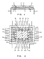
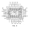
- Figs. 2 and 3 views of opposite sides of another type of integrated circuit memory package are shown.
- the package shown in Figs. 2 and 3 will be a plastic leaded chip carrier or PLCC.
- PLCC plastic leaded chip carrier
- Such a package is suited for surface mounting without leads that extend through holes in a printed circuit board.
- the partially completed package shown in Figs. 2 and 3 differs from the DIP package in Fig. 1 in that the package of Figs. 2 and 3 has leads extending from four sides thereof instead of the leads extending from the two sides of a DIP package.
- a semiconductor integrated circuit memory chip 20 is suitably attached to the central portion of a lead frame 21.
- the lead frame 21 has a plurality of connecting leads 91-106 extending therefrom which, at this stage of the manufacture of the package, are all physically and electrically connected together by the metal of the lead frame which will be cut later in the manufacturing process.
- a plurality of circuit termination points 31-46 on chip 20 are connected by a plurality of wire bonds 50 to the individual portions of the lead frame 21 which will comprise the leads 91-106.
- FIG. 3 shows a view of this subassembly after a 180 degree rotation about this imaginary vertical axis.
- another integrated circuit memory chip 60 is attached to the central portion of an opposite side of the same lead frame 21.
- the circuit termination points on chip 60 are a mirror image of the corresponding circuit termination points on chip 20. That is, the sets of circuit termination points, starting with the lowest numbered circuit termination point and ending with the highest numbered circuit termination point on each of the chips 20 and 60 are mirror images of each other. Accordingly, the lowest numbered circuit termination points 31 (on chip 20) and 61 (on chip 60) are connected by wire bonds to the same connecting lead (91) on the lead frame 21 and the other pairs of corresponding termination points on the two chips are connected to the same connecting lead.
- the dashed line 80 in each of Figs. 2 and 3 represents the mould outline for encapsulation of the subassembly in a suitable material.
- a technique has been shown and described for mounting a first integrated circuit chip on one side of a lead frame and complementing this subassembly by the addition of a mirror image second integrated circuit chip mounted on the opposite side of the lead frame.
- This assembly is then encapsulated in an appropriate material, such as plastic.
- Memory chips are especially suitably for this mounting technique, which is adaptable to pinned, leaded, and surface mount integrated circuit packages.
Landscapes
- Physics & Mathematics (AREA)
- Condensed Matter Physics & Semiconductors (AREA)
- General Physics & Mathematics (AREA)
- Engineering & Computer Science (AREA)
- Computer Hardware Design (AREA)
- Microelectronics & Electronic Packaging (AREA)
- Power Engineering (AREA)
- Lead Frames For Integrated Circuits (AREA)
- Wire Bonding (AREA)
- Semiconductor Memories (AREA)
Applications Claiming Priority (2)
| Application Number | Priority Date | Filing Date | Title |
|---|---|---|---|
| US79489985A | 1985-11-04 | 1985-11-04 | |
| US794899 | 1985-11-04 |
Publications (2)
| Publication Number | Publication Date |
|---|---|
| EP0221496A2 true EP0221496A2 (fr) | 1987-05-13 |
| EP0221496A3 EP0221496A3 (fr) | 1987-10-28 |
Family
ID=25164034
Family Applications (1)
| Application Number | Title | Priority Date | Filing Date |
|---|---|---|---|
| EP86114966A Withdrawn EP0221496A3 (fr) | 1985-11-04 | 1986-10-28 | Empaquetage pour circuit intégré |
Country Status (2)
| Country | Link |
|---|---|
| EP (1) | EP0221496A3 (fr) |
| JP (1) | JPS62109333A (fr) |
Cited By (11)
| Publication number | Priority date | Publication date | Assignee | Title |
|---|---|---|---|---|
| GB2196475A (en) * | 1986-09-23 | 1988-04-27 | Royal Ordnance Plc | Timer package |
| US4974053A (en) * | 1988-10-06 | 1990-11-27 | Mitsubishi Denki Kabushiki Kaisha | Semiconductor device for multiple packaging configurations |
| EP0408779A1 (fr) * | 1989-07-18 | 1991-01-23 | International Business Machines Corporation | Module semi-conducteur de mémoire à haute densité |
| EP0474224A1 (fr) * | 1990-09-06 | 1992-03-11 | Hitachi, Ltd. | Dispositif semi-conducteur comprenant une pluralité de puces semi-conductrices |
| US5296737A (en) * | 1990-09-06 | 1994-03-22 | Hitachi, Ltd. | Semiconductor device with a plurality of face to face chips |
| EP0608440A1 (fr) * | 1992-12-18 | 1994-08-03 | Fujitsu Limited | Dispositif semi-conducteur comprenant une pluralité de puces avec des arrangements de circuit identiques encapsulé dans un empaquetage |
| EP0774162A1 (fr) * | 1994-06-28 | 1997-05-21 | Intel Corporation | Fabrication de boitiers de puces a circuits integres, a doubles faces, a soudures de connexion, utilisant des soudures de connexion decalees et des cavites de blocs auxiliaires |
| EP0847086A2 (fr) * | 1996-12-03 | 1998-06-10 | Texas Instruments Incorporated | Améliorations dans ou relatives aux dispositifs semi-conducteurs |
| US5880531A (en) * | 1993-06-11 | 1999-03-09 | Hitachi, Ltd. | Lead on chip semiconductor memory device with multiple bit configuration |
| US7148578B2 (en) | 2001-07-10 | 2006-12-12 | Samsung Electronics Co., Ltd. | Semiconductor multi-chip package |
| US7282789B2 (en) * | 1998-03-31 | 2007-10-16 | Micron Technology, Inc. | Back-to-back semiconductor device assemblies |
Citations (5)
| Publication number | Priority date | Publication date | Assignee | Title |
|---|---|---|---|---|
| JPS5617050A (en) * | 1979-07-20 | 1981-02-18 | Nec Corp | Semiconductor device |
| JPS5662351A (en) * | 1979-10-26 | 1981-05-28 | Hitachi Ltd | Semiconductor device for memory |
| JPS56137665A (en) * | 1980-03-31 | 1981-10-27 | Chiyou Lsi Gijutsu Kenkyu Kumiai | Semiconductor device |
| JPS58130553A (ja) * | 1982-01-29 | 1983-08-04 | Toshiba Corp | 半導体装置 |
| JPS6028256A (ja) * | 1983-07-26 | 1985-02-13 | Fujitsu Ltd | 半導体装置 |
Family Cites Families (1)
| Publication number | Priority date | Publication date | Assignee | Title |
|---|---|---|---|---|
| JPS6037758A (ja) * | 1983-08-10 | 1985-02-27 | Nec Corp | 半導体装置 |
-
1986
- 1986-10-03 JP JP61234709A patent/JPS62109333A/ja active Pending
- 1986-10-28 EP EP86114966A patent/EP0221496A3/fr not_active Withdrawn
Patent Citations (5)
| Publication number | Priority date | Publication date | Assignee | Title |
|---|---|---|---|---|
| JPS5617050A (en) * | 1979-07-20 | 1981-02-18 | Nec Corp | Semiconductor device |
| JPS5662351A (en) * | 1979-10-26 | 1981-05-28 | Hitachi Ltd | Semiconductor device for memory |
| JPS56137665A (en) * | 1980-03-31 | 1981-10-27 | Chiyou Lsi Gijutsu Kenkyu Kumiai | Semiconductor device |
| JPS58130553A (ja) * | 1982-01-29 | 1983-08-04 | Toshiba Corp | 半導体装置 |
| JPS6028256A (ja) * | 1983-07-26 | 1985-02-13 | Fujitsu Ltd | 半導体装置 |
Non-Patent Citations (6)
| Title |
|---|
| IBM TECHNICAL DISCLOSURE BULLETIN, vol. 27, no. 4B, September 1984, pages 2389-2390, Armonk, N.Y., US; P.V. ROBOCK: "Stackable plastic semiconductor chip carrier" * |
| PATENT ABSTRACTS OF JAPAN, vol. 5, no. 125 (E-69)[797], 12th August 1981; & JP-A-56 062 351 (HITACHI SEISAKUSHO K.K.) 28-05-1981 * |
| PATENT ABSTRACTS OF JAPAN, vol. 5, no. 66 (E-55)[738], 2nd May 1981; & JP-A-56 017 050 (NIPPON DENKI K.K.) 18-02-1981 * |
| PATENT ABSTRACTS OF JAPAN, vol. 6, no. 16 (E-92)[894], 29th January 1982; & JP-A-56 137 665 (CHO LSI GIJUTSU KENKYU KUMIAI) 27-10-1981 * |
| PATENT ABSTRACTS OF JAPAN, vol. 7, no. 239 (E-206)[1384], 25th October 1983; & JP-A-58 130 553 (TOKYO SHIBAURA DENKI K.K.) 04-08-1983 * |
| PATENT ABSTRACTS OF JAPAN, vol. 9, no. 147 (E-323)[1870], 21st June 1985; & JP-A-60 028 256 (FUJITSU K.K.) 13-02-1985 * |
Cited By (21)
| Publication number | Priority date | Publication date | Assignee | Title |
|---|---|---|---|---|
| GB2196475B (en) * | 1986-09-23 | 1990-01-10 | Royal Ordnance Plc | Semiconductor chip constructions |
| GB2196475A (en) * | 1986-09-23 | 1988-04-27 | Royal Ordnance Plc | Timer package |
| US4974053A (en) * | 1988-10-06 | 1990-11-27 | Mitsubishi Denki Kabushiki Kaisha | Semiconductor device for multiple packaging configurations |
| EP0408779A1 (fr) * | 1989-07-18 | 1991-01-23 | International Business Machines Corporation | Module semi-conducteur de mémoire à haute densité |
| EP0474224A1 (fr) * | 1990-09-06 | 1992-03-11 | Hitachi, Ltd. | Dispositif semi-conducteur comprenant une pluralité de puces semi-conductrices |
| US5296737A (en) * | 1990-09-06 | 1994-03-22 | Hitachi, Ltd. | Semiconductor device with a plurality of face to face chips |
| EP0608440A1 (fr) * | 1992-12-18 | 1994-08-03 | Fujitsu Limited | Dispositif semi-conducteur comprenant une pluralité de puces avec des arrangements de circuit identiques encapsulé dans un empaquetage |
| US5508565A (en) * | 1992-12-18 | 1996-04-16 | Fujitsu Limited | Semiconductor device having a plurality of chips having identical circuit arrangement sealed in package |
| US5880531A (en) * | 1993-06-11 | 1999-03-09 | Hitachi, Ltd. | Lead on chip semiconductor memory device with multiple bit configuration |
| EP0774162A1 (fr) * | 1994-06-28 | 1997-05-21 | Intel Corporation | Fabrication de boitiers de puces a circuits integres, a doubles faces, a soudures de connexion, utilisant des soudures de connexion decalees et des cavites de blocs auxiliaires |
| EP0774162A4 (fr) * | 1994-06-28 | 1997-07-30 | Intel Corp | Fabrication de boitiers de puces a circuits integres, a doubles faces, a soudures de connexion, utilisant des soudures de connexion decalees et des cavites de blocs auxiliaires |
| EP0847086A2 (fr) * | 1996-12-03 | 1998-06-10 | Texas Instruments Incorporated | Améliorations dans ou relatives aux dispositifs semi-conducteurs |
| EP0847086A3 (fr) * | 1996-12-03 | 2000-07-26 | Texas Instruments Incorporated | Améliorations dans ou relatives aux dispositifs semi-conducteurs |
| US7282789B2 (en) * | 1998-03-31 | 2007-10-16 | Micron Technology, Inc. | Back-to-back semiconductor device assemblies |
| US7148578B2 (en) | 2001-07-10 | 2006-12-12 | Samsung Electronics Co., Ltd. | Semiconductor multi-chip package |
| DE10231385B4 (de) * | 2001-07-10 | 2007-02-22 | Samsung Electronics Co., Ltd., Suwon | Halbleiterchip mit Bondkontaktstellen und zugehörige Mehrchippackung |
| US7453159B2 (en) | 2001-07-10 | 2008-11-18 | Samsung Electronics Co., Ltd. | Semiconductor chip having bond pads |
| US7541682B2 (en) | 2001-07-10 | 2009-06-02 | Samsung Electronics Co., Ltd. | Semiconductor chip having bond pads |
| US7547977B2 (en) | 2001-07-10 | 2009-06-16 | Samsung Electronics Co., Ltd. | Semiconductor chip having bond pads |
| US7576440B2 (en) | 2001-07-10 | 2009-08-18 | Samsung Electronics Co., Ltd. | Semiconductor chip having bond pads and multi-chip package |
| US7825523B2 (en) | 2001-07-10 | 2010-11-02 | Samsung Electronics Co., Ltd. | Semiconductor chip having bond pads |
Also Published As
| Publication number | Publication date |
|---|---|
| EP0221496A3 (fr) | 1987-10-28 |
| JPS62109333A (ja) | 1987-05-20 |
Similar Documents
| Publication | Publication Date | Title |
|---|---|---|
| US5656856A (en) | Reduced noise semiconductor package stack | |
| US5247423A (en) | Stacking three dimensional leadless multi-chip module and method for making the same | |
| US5563446A (en) | Surface mount peripheral leaded and ball grid array package | |
| US5413970A (en) | Process for manufacturing a semiconductor package having two rows of interdigitated leads | |
| US4763188A (en) | Packaging system for multiple semiconductor devices | |
| US7408255B2 (en) | Assembly for stacked BGA packages | |
| US5998865A (en) | Loc simm | |
| US6507107B2 (en) | Semiconductor/printed circuit board assembly | |
| US6313998B1 (en) | Circuit board assembly having a three dimensional array of integrated circuit packages | |
| US5468994A (en) | High pin count package for semiconductor device | |
| KR0127873B1 (ko) | 연부-장착된 반도체 집적 회로 디바이스용 표면-장착 팩키지 | |
| US5684330A (en) | Chip-sized package having metal circuit substrate | |
| US6538313B1 (en) | IC package with integral substrate capacitor | |
| US5260601A (en) | Edge-mounted, surface-mount package for semiconductor integrated circuit devices | |
| JP2910670B2 (ja) | 半導体実装構造 | |
| US5227995A (en) | High density semiconductor memory module using split finger lead frame | |
| US6104095A (en) | Printed circuit board and chip-on-board packages using same | |
| US6107121A (en) | Method of making interconnections between a multi-layer chip stack to a printed circuit board in a ceramic package | |
| US5349235A (en) | High density vertically mounted semiconductor package | |
| EP0221496A2 (fr) | Empaquetage pour circuit intégré | |
| JPH0730059A (ja) | マルチチップモジュール | |
| US5706172A (en) | Stacked semiconductor package having supporting bars and a socket therefor | |
| KR100235495B1 (ko) | 반도체 장치 | |
| US20020023766A1 (en) | Method and apparatus for polygonal heat slug | |
| JPH0969587A (ja) | Bga型半導体装置及びbgaモジュール |
Legal Events
| Date | Code | Title | Description |
|---|---|---|---|
| PUAI | Public reference made under article 153(3) epc to a published international application that has entered the european phase |
Free format text: ORIGINAL CODE: 0009012 |
|
| AK | Designated contracting states |
Kind code of ref document: A2 Designated state(s): DE FR GB |
|
| PUAL | Search report despatched |
Free format text: ORIGINAL CODE: 0009013 |
|
| AK | Designated contracting states |
Kind code of ref document: A3 Designated state(s): DE FR GB |
|
| 17P | Request for examination filed |
Effective date: 19870818 |
|
| 17Q | First examination report despatched |
Effective date: 19890502 |
|
| STAA | Information on the status of an ep patent application or granted ep patent |
Free format text: STATUS: THE APPLICATION HAS BEEN WITHDRAWN |
|
| 18W | Application withdrawn |
Withdrawal date: 19891010 |
|
| R18W | Application withdrawn (corrected) |
Effective date: 19891010 |
|
| RIN1 | Information on inventor provided before grant (corrected) |
Inventor name: SINGH, PRATAP Inventor name: OVERFIELD, RICHARD BLEWER |