EP0218288B1 - Sowohl als N-Kanal-MOS-Transistor als auch als P-Kanal-MOS-Transistor verwendbare MOS-Leistungsvorrichtung - Google Patents
Sowohl als N-Kanal-MOS-Transistor als auch als P-Kanal-MOS-Transistor verwendbare MOS-Leistungsvorrichtung Download PDFInfo
- Publication number
- EP0218288B1 EP0218288B1 EP86201593A EP86201593A EP0218288B1 EP 0218288 B1 EP0218288 B1 EP 0218288B1 EP 86201593 A EP86201593 A EP 86201593A EP 86201593 A EP86201593 A EP 86201593A EP 0218288 B1 EP0218288 B1 EP 0218288B1
- Authority
- EP
- European Patent Office
- Prior art keywords
- capacitor
- control signal
- mos
- voltage
- channel
- Prior art date
- Legal status (The legal status is an assumption and is not a legal conclusion. Google has not performed a legal analysis and makes no representation as to the accuracy of the status listed.)
- Expired
Links
- 239000003990 capacitor Substances 0.000 claims description 25
- 230000008878 coupling Effects 0.000 claims 1
- 238000010168 coupling process Methods 0.000 claims 1
- 238000005859 coupling reaction Methods 0.000 claims 1
- 238000007599 discharging Methods 0.000 claims 1
- 238000005516 engineering process Methods 0.000 claims 1
- 238000010521 absorption reaction Methods 0.000 description 3
- 239000013641 positive control Substances 0.000 description 3
- 230000008033 biological extinction Effects 0.000 description 2
- 238000010586 diagram Methods 0.000 description 2
- 239000013642 negative control Substances 0.000 description 2
- 230000007935 neutral effect Effects 0.000 description 2
- 230000009286 beneficial effect Effects 0.000 description 1
- 230000002457 bidirectional effect Effects 0.000 description 1
- 238000010276 construction Methods 0.000 description 1
- 230000001419 dependent effect Effects 0.000 description 1
- 230000010354 integration Effects 0.000 description 1
Images

Classifications
-
- H—ELECTRICITY
- H03—ELECTRONIC CIRCUITRY
- H03K—PULSE TECHNIQUE
- H03K17/00—Electronic switching or gating, i.e. not by contact-making and –breaking
- H03K17/51—Electronic switching or gating, i.e. not by contact-making and –breaking characterised by the components used
- H03K17/56—Electronic switching or gating, i.e. not by contact-making and –breaking characterised by the components used by the use, as active elements, of semiconductor devices
- H03K17/687—Electronic switching or gating, i.e. not by contact-making and –breaking characterised by the components used by the use, as active elements, of semiconductor devices the devices being field-effect transistors
- H03K17/693—Switching arrangements with several input- or output-terminals, e.g. multiplexers, distributors
Definitions
- the present invention relates to an MOS power device usable as an MOS transistor with an N channel and as an MOS transistor with a P channel.
- transistors with N channels which can be driven in conduction by means of positive gate voltage in relation to the source voltage
- MOS transistors with P channels which can be driven in conduction by means of negative gate voltage in relation to the source voltage.
- the former are generally preferable to the latter from the viewpoint of cost and commutation speed and because they are easy to integrate.
- PWM pulse width modulation
- bridge actuators which preferably include two P channel MOS transistors and two N channel MOS transistors arranged in a bridge with drain in common between a positive supply lead and a negative supply lead.
- the two N channel transistors are made to conduct by applying to the gate a voltage which is positive in relation to the negative supply lead while the two P channel transistors are made to conduct by applying to the gate a voltage which is negative in relation to the positive supply lead.
- Two different ways of controlling are thus provided for the two types of transistors.
- a bridge circuit for bidirectional control of a D.C. motor is also known from US-A-4 454 454 and comprises four N-channel devices, two of which have a gate voltage provided by a converter, which is higher than that of the general power supply.
- the primary object of the present invention is to accomplish an MOS power device which would be usable and controllable as a P-channel MOS transistor without suffering from the usual penalties of cost, speed and integration difficulty typical of transistors of this type.
- Another object of the present invention is to accomplish an MOS power device usable and controllable either as a P-channel MOS transistor or as an N-channel MOS transistor, in particular in such a manner as to be employed in both the provided versions in a bridge structure of the type mentioned above.
- an MOS device based on an N-channel power switch and thus in possession of the requisites of cost and switching speed of devices of that type is made usable in N or P versions by being provided with two independent inputs of which one, the first abovementioned, may be considered and used as a gate input for an N channel transistor, i.e. controllable with positive signal in relation to the negative supply lead, and the other, the second abovementioned, may be considered and used as a gate input for a P-channel transistor, i.e. controllable with a signal which is negative in relation to the positive supply lead.
- a bridge structure can provide four identical devices in accordance with the invention, two used as N-channel transistors and two as P-channel transistors.
- the device lends itself to control with a low-level logic circuit such as the one obtainable at the output by a microprocessor.
- the MOS device illustrated therein consists of a single integrable set 1 from which issues a terminal 2 for positive supply, a terminal 3 for negative supply or reference, two terminals 4 and 5 connected through an external capacitor of relatively large capacity, e.g. 0.1 ⁇ F, a terminal 6 for control of the N-channel type and a terminal 7 for control of the P-channel type.
- the integrable set 1 includes as its basic element a power switch of the N channel MOS type denominated Q11 which has its drain connected to a positive supply lead 8 extending from the terminal 2 and its source connected to a negative supply or reference lead 9 extending from the terminal 3 to the terminal 5.
- Gate control of the power switch Q11 is provided by two CMOS inverters I1 and I2 having reversed polarity connected cascadewise of which the first comprises an N-channel switch element Q5 and a P-channel switch element Q6 and the second, designed to deliver a higher current suitable for control of Q11, comprises three N-channel switch elements Q7, Q8 and Q10 and a P-channel switch element Q9.
- the inverter I1 includes furthermore a capacitor C2, e.g. of 10pF, and a diode D2 for the purposes which will be set forth below.
- Supply for the two inverters at reduced voltage in relation to that of the power switch Q11 is supplied by the external capacitor C loaded by the positive supply lead 8 through a resistor R1 and a diode D3 and is stabilized by a Zener diode Z1.
- the input of the inverter I1 is connected to the terminal 6 which is designed to receive a control signal with positive voltage in relation to the negative lead 9, i.e. a control signal suitable for an N-channel transistor. Since the two inverters have reversed polarity, the above control signal is again with the same polarity but amplified on the gate of the power switch Q11 which in the presence of said signal on the terminal 6 is thus correctly made to operate in the manner peculiar to an N-channel device.
- the input of the switch I1 is connected to the negative lead 9 through a capacitor C1 which is the essential component for operation of the power device 1 in the manner of a P-channel transistor as will be made clear below.
- the terminal 7 which is designed to receive a voltage control signal negative in relation to the positive lead 8, which is protected by the Zener diode Z2, i.e. a control signal suitable for a P-channel transistor, is connected to the gate of a P-channel MOS switch element Q1 which has its source connected to the positive lead 8 and its drain connected to the negative lead 9 through a resistor R2, e.g. of 33K, in parallel with which is placed a Zener diode Z3.
- the drain of the element Q1 is also connected to the gate of an N-channel MOS switch element Q4 which has its drain connected to the supply terminal 4 and its source connected to the negative lead 9 through the drain-source connection of an N-channel MOS switch element Q3.
- the gate of Q3 is connected to the negative lead 9 through a resistor R3, e.g. of 100K, and is also connected through a capacitor C3, e.g. of 10pF, to the drain of a P-channel MOS switch element which has its source connected to the control terminal 7 and its gate connected to the positive terminal through a capacitor C4, e.g. of 10pF, and to the control terminal 7 through a resistor R4, e.g. of 47K.
- the drain of Q2 is connected to the output of the inverter I1 through a resistance R5, e.g. of 47K, stabilized by a Zener diode Z4 and a capacitor C5, e.g. of 40pF, with associated diode D1.
- the described device is capable of operating both as a power transistor with a positive control signal in relation to the lead 9 on the terminal 6, in which case it behaves like an N-type transistor, and with a negative control signal in relation to the lead 8 on the terminal 7, in which case it behaves like a P-type transistor but having all the beneficial characteristics of cost, switching speed and integrability of an N-type device which in reality it is in its power part (switch Q11).
- the presence of C2 and D2 permits the device 1 to operate with control signals at 6 with a voltage lower than that between the terminals 4 and 5 hence small enough to permit control by a microprocessor.
- the positive fronts of the control signal on the terminal 6 in fact, charge the capacitor C2 at the lower voltage of the control signal and causes turn-off of Q6, while the diode D2 prevents passage of current from the terminal 4 to the gate of Q6 once C2 has been charged; the subsequent negative fronts of the control signal cause discharge of C2 and consequent turn-on of Q6, while Q5 is turned-off.
- control part (inverters I1 and I2) of the device absorbs a very small current supplied by the external capacitor C only when coinciding with the switching fronts of the control signal. Current absorption is thus very small and dependent upon the frequency of said switching fronts.
- the negative front thereof causes in turn momentary conduction of Q1, which generates on R2 a voltage drop which puts Q4 in conduction which is operating as a source follower.
- the current of Q4 rapidly charges the capacitor C1 at the ends of which is stabilized a positive voltage equivalent basically to a positive control signal applied to the terminal 6.
- the device 1 behaves as though a control signal for an N-channel transistor were applied thereto, i.e. the power switch Q11 is placed in conduction in accordance with the modes and characteristics of an N-channel transistor.
- the conduction of Q11 causes reduction of the voltage of the positive terminal 2 in relation to that of the reference terminal 3 so that the drain-source voltage of the element Q1 is reduced and causes extinction of Q1.
- the input voltage of the two inverters I1, I2 remains however steady thanks to the charging of the capacitor C1.
- Said positive front thus causes momentary conduction of Q2 whose current generates on the resistor R5 a positive voltage drop which causes conduction of Q3 through which the capacitor C1 can discharge to bring the device 1 back to neutral position.
- Q2 also then returns to neutral when through C4 its gate voltage returns up to a value such as to cause extinction of Q2.
- the device 1 may be controlled in the manner of an N-channel transistor or in the manner of a P-channel transistor depending on whether the input terminal 6 or the input terminal 7 is used.
- Several of the same devices controlled in different manners may thus be used to form complex structures which need both N-channel MOS transistors and P-channel MOS transistors.
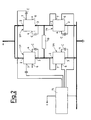
- the example shown in FIG 2 may be considered typical where there is illustrated a load actuator system 10 which is accomplished in the form of a bridge structure including four MOS power devices like the one shown in FIG 1 of which two, indicated by reference 1N, are employed and controlled as N-channel transistors and the other two, indicated with reference 1P, are employed as channel P transistors.
- a microprocessor 11 controls the actuator thanks to the low level features of the control signal ensured by the capacitor C2 an the diode D2. It should be noted how the transistors 1N have the terminals 2 and 7 connected together. This has the purpose of keeping surely interdicted the circuit elements Q1-Q4 of the two transistors in N-channel operation.
Landscapes
- Electronic Switches (AREA)
- Dc-Dc Converters (AREA)
Claims (6)
- MOS-Leistungsvorrichtung,
gekennzeichnet durch
einen N-Kanal-Leistungsschalter (Q11) mit Drain und Source, die jeweils an eine positive Stromversorgungsleitung (8) bzw. an eine negative Stromversorgungsleitung (9) angeschlossen sind, zwei in Kaskade geschaltete Inverter (I1,I2), die der Gate-Steuerung des Leistungsschalters (Q11) zugeordnet sind und die mit einer bezüglich der dem Leistungsschalter (Q11) zugeführten Spannung verminderten Spannung versorgt werden, wobei die verminderte Spannung durch einen externen Kondensator (C) geliefert wird, der zwischen die Stromversorgungsleitungen (8,9) geschaltet ist, und zwei Eingänge für die Inverter, wobei ein erster Eingang (6) für ein erstes Steuersignal mit gegenüber der negativen Stromversorgungsleitung (9) positiven Spannung ausgelegt ist und der zweite Eingang (7) für ein zweites Steuersignal mit gegenüber der positiven Stromversorgungsleitung (8) negativer Spannung ausgelegt ist, und wobei ein zwischen den ersten Eingang (6) und die negative Stromversorgungsleitung (9) geschalteter Kondensator (C1) vorgesehen ist, und wobei Schalteinrichtungen (Q1,Q2,Q3,Q4) zwischen den zweiten Eingang (7) und den Kondensator (C1) geschaltet sind, um dem zweiten Steuersignal zu ermöglichen, den Kondensator (C1) auf eine positive Spannung gegenüber der negativen Stromversorgungsleitung (9) zu laden und nachfolgend den Kondensator (C1) zu entladen. - Vorrichtung nach Anspruch 1,
dadurch gekennzeichnet,
daß die Inverter (I1,I2) in CMOS-Technologie ausgeführt sind. - Vorrichtung nach Anspruch 1,
dadurch gekennzeichnet,
daß es eine kapazitative Kopplungseinrichtung (C2) aufweist, die den Invertern (I1,I2) zugeordnet ist, und die durch das erste Steuersignal bei einer Spannung, die geringer ist als die verminderte Spannung, aufzuladen ist. - Vorrichtung nach Anspruch 1,
dadurch gekennzeichnet,
daß die Schalteinrichtungen (Q1,Q2,Q3,Q4) erste durch das zweite Steuersignal angesteuerte MOS-Schalter (Q1,Q4) aufweisen, um das Aufladen des Kondensators (C1) zu bewirken, und zweite, nachfolgend durch das zweite Steuersignal angesteuerte MOS-Schalter (Q2,Q3) aufweisen, um das Entladen des Kondensators (C1) zu bewirken. - Vorrichtung nach Anspruch 4,
dadurch gekennzeichnet,
daß die ersten Schalter (Q1,Q4) ein erstes und ein zweites MOS-Schalterelement (Q1,Q4) aufweisen, die in Sourcefolger-Anordnung geschaltet sind, wobei das erste Schalterelement (Q1) durch das zweite Steuersignal gesteuert wird und wobei das zweite Schalterelement (Q4) ausgelegt ist, den Kondensator (C1) aufzuladen. - Vorrichtung nach Anspruch 4,
dadurch gekennzeichnet,
daß die zweiten Schalter (Q2,Q3) ein durch das zweite Steuersignal gesteuertes drittes Schalterelement (Q2) und ein viertes Schalterelement (Q3), das zum Entladen des Kondensators (C1) ausgelegt ist, aufweisen.
Applications Claiming Priority (2)
| Application Number | Priority Date | Filing Date | Title |
|---|---|---|---|
| IT2238085 | 1985-10-07 | ||
| IT22380/85A IT1185998B (it) | 1985-10-07 | 1985-10-07 | Dispositivo mcs di potenza utilizzabile sia come transistore mos a canale n che come transistore mos a canale p |
Publications (3)
| Publication Number | Publication Date |
|---|---|
| EP0218288A2 EP0218288A2 (de) | 1987-04-15 |
| EP0218288A3 EP0218288A3 (en) | 1989-03-08 |
| EP0218288B1 true EP0218288B1 (de) | 1992-04-22 |
Family
ID=11195490
Family Applications (1)
| Application Number | Title | Priority Date | Filing Date |
|---|---|---|---|
| EP86201593A Expired EP0218288B1 (de) | 1985-10-07 | 1986-09-16 | Sowohl als N-Kanal-MOS-Transistor als auch als P-Kanal-MOS-Transistor verwendbare MOS-Leistungsvorrichtung |
Country Status (5)
| Country | Link |
|---|---|
| US (1) | US4764692A (de) |
| EP (1) | EP0218288B1 (de) |
| JP (1) | JP2504966B2 (de) |
| DE (1) | DE3684981D1 (de) |
| IT (1) | IT1185998B (de) |
Families Citing this family (4)
| Publication number | Priority date | Publication date | Assignee | Title |
|---|---|---|---|---|
| IT1190436B (it) * | 1985-12-13 | 1988-02-16 | Zambon Spa | Processo stereoselettivo per la preparazione di composti carbonilici alfa,beta-disostituiti otticamente attivi |
| IT1215501B (it) * | 1987-05-18 | 1990-02-14 | Sgs Microelettronica Spa | Circuito a ponte a transistori moscon ricircolo veloce di corrente abassa diddipazione. |
| US4982120A (en) * | 1989-07-03 | 1991-01-01 | Dell Corporate Services Corporation | Power supply decoupling mechanism for integrated circuits |
| DE59505122D1 (de) * | 1994-03-24 | 1999-03-25 | Siemens Ag | Verlustarme integrierte schaltung mit reduziertem takthub |
Family Cites Families (4)
| Publication number | Priority date | Publication date | Assignee | Title |
|---|---|---|---|---|
| US4347445A (en) * | 1979-12-31 | 1982-08-31 | Exxon Research And Engineering Co. | Floating hybrid switch |
| GB2069268A (en) * | 1980-01-24 | 1981-08-19 | Centre Electron Horloger | Sampling circuit |
| US4454454A (en) * | 1983-05-13 | 1984-06-12 | Motorola, Inc. | MOSFET "H" Switch circuit for a DC motor |
| US4542310A (en) * | 1983-06-29 | 1985-09-17 | International Business Machines Corporation | CMOS bootstrapped pull up circuit |
-
1985
- 1985-10-07 IT IT22380/85A patent/IT1185998B/it active
-
1986
- 1986-09-16 DE DE8686201593T patent/DE3684981D1/de not_active Expired - Lifetime
- 1986-09-16 EP EP86201593A patent/EP0218288B1/de not_active Expired
- 1986-09-18 US US06/908,691 patent/US4764692A/en not_active Expired - Lifetime
- 1986-10-07 JP JP61238978A patent/JP2504966B2/ja not_active Expired - Fee Related
Also Published As
| Publication number | Publication date |
|---|---|
| JP2504966B2 (ja) | 1996-06-05 |
| EP0218288A2 (de) | 1987-04-15 |
| IT1185998B (it) | 1987-11-18 |
| US4764692A (en) | 1988-08-16 |
| JPS6292518A (ja) | 1987-04-28 |
| IT8522380A0 (it) | 1985-10-07 |
| EP0218288A3 (en) | 1989-03-08 |
| DE3684981D1 (de) | 1992-05-27 |
Similar Documents
| Publication | Publication Date | Title |
|---|---|---|
| US4459498A (en) | Switch with series-connected MOS-FETs | |
| US5051881A (en) | Voltage multiplier | |
| US4445055A (en) | Circuit arrangement for controlling a power field-effect switching transistor | |
| EP0703666B1 (de) | Steuerschaltung mit einem Pegelschieber zum Schalten eines eletronischen Schalters | |
| US4972130A (en) | Multipurpose, internally configurable integrated circuit for driving in a switching mode external inductive loads according to a selectable connection scheme | |
| EP0070158B1 (de) | Spannungsspitzen-Begrenzerschaltung geringen Verlustes für Leistungsschalttransistoren | |
| JPH07105448B2 (ja) | Mos型集積回路 | |
| EP0130273B1 (de) | FET-Steuerungsschaltung | |
| JPH0561807B2 (de) | ||
| US5138186A (en) | Solid state switch with last state memory | |
| US5381044A (en) | Bootstrap circuit for driving a power MOS transistor | |
| US4717845A (en) | TTL compatible CMOS input circuit | |
| US5534769A (en) | Synchronous rectifying circuit | |
| KR950002233A (ko) | 노이즈를 감소하는 출력단을 구비한 집적회로 | |
| US4764692A (en) | MOS power device usable both as an N-channel MOS transistor and as a P-channel MOS transistor | |
| RU2152127C1 (ru) | Силовой ключ на мдп-транзисторе | |
| US6130569A (en) | Method and apparatus for a controlled transition rate driver | |
| EP1001537B1 (de) | Steuerschaltung | |
| JPS61166223A (ja) | 複合形スイツチ回路 | |
| EP0685941B1 (de) | Bootstrapschaltung | |
| JP3367536B2 (ja) | サーボモータの駆動制御回路 | |
| JPH0698574A (ja) | モータ駆動回路 | |
| JPS6477220A (en) | Driving circuit for mos-fet | |
| JPH025613A (ja) | スリーステート出力回路 | |
| JPH043618B2 (de) |
Legal Events
| Date | Code | Title | Description |
|---|---|---|---|
| PUAI | Public reference made under article 153(3) epc to a published international application that has entered the european phase |
Free format text: ORIGINAL CODE: 0009012 |
|
| AK | Designated contracting states |
Kind code of ref document: A2 Designated state(s): DE FR GB NL |
|
| RAP1 | Party data changed (applicant data changed or rights of an application transferred) |
Owner name: SGS-THOMSON MICROELECTRONICS S.P.A. |
|
| PUAL | Search report despatched |
Free format text: ORIGINAL CODE: 0009013 |
|
| AK | Designated contracting states |
Kind code of ref document: A3 Designated state(s): DE FR GB NL |
|
| 17P | Request for examination filed |
Effective date: 19890615 |
|
| RAP1 | Party data changed (applicant data changed or rights of an application transferred) |
Owner name: SGS-THOMSON MICROELECTRONICS S.R.L. |
|
| 17Q | First examination report despatched |
Effective date: 19900801 |
|
| GRAA | (expected) grant |
Free format text: ORIGINAL CODE: 0009210 |
|
| AK | Designated contracting states |
Kind code of ref document: B1 Designated state(s): DE FR GB NL |
|
| REF | Corresponds to: |
Ref document number: 3684981 Country of ref document: DE Date of ref document: 19920527 |
|
| ET | Fr: translation filed | ||
| PLBE | No opposition filed within time limit |
Free format text: ORIGINAL CODE: 0009261 |
|
| STAA | Information on the status of an ep patent application or granted ep patent |
Free format text: STATUS: NO OPPOSITION FILED WITHIN TIME LIMIT |
|
| 26N | No opposition filed | ||
| REG | Reference to a national code |
Ref country code: FR Ref legal event code: D6 |
|
| PGFP | Annual fee paid to national office [announced via postgrant information from national office to epo] |
Ref country code: NL Payment date: 20010927 Year of fee payment: 16 |
|
| REG | Reference to a national code |
Ref country code: GB Ref legal event code: IF02 |
|
| PGFP | Annual fee paid to national office [announced via postgrant information from national office to epo] |
Ref country code: GB Payment date: 20020215 Year of fee payment: 16 |
|
| PGFP | Annual fee paid to national office [announced via postgrant information from national office to epo] |
Ref country code: FR Payment date: 20020225 Year of fee payment: 16 |
|
| PGFP | Annual fee paid to national office [announced via postgrant information from national office to epo] |
Ref country code: DE Payment date: 20020227 Year of fee payment: 16 |
|
| PG25 | Lapsed in a contracting state [announced via postgrant information from national office to epo] |
Ref country code: GB Free format text: LAPSE BECAUSE OF NON-PAYMENT OF DUE FEES Effective date: 20020916 |
|
| PG25 | Lapsed in a contracting state [announced via postgrant information from national office to epo] |
Ref country code: NL Free format text: LAPSE BECAUSE OF NON-PAYMENT OF DUE FEES Effective date: 20030401 Ref country code: DE Free format text: LAPSE BECAUSE OF NON-PAYMENT OF DUE FEES Effective date: 20030401 |
|
| GBPC | Gb: european patent ceased through non-payment of renewal fee |
Effective date: 20020916 |
|
| PG25 | Lapsed in a contracting state [announced via postgrant information from national office to epo] |
Ref country code: FR Free format text: LAPSE BECAUSE OF NON-PAYMENT OF DUE FEES Effective date: 20030603 |
|
| REG | Reference to a national code |
Ref country code: FR Ref legal event code: ST |