EP0217469A1 - Display arrangement with improved drive - Google Patents
Display arrangement with improved drive Download PDFInfo
- Publication number
- EP0217469A1 EP0217469A1 EP86201660A EP86201660A EP0217469A1 EP 0217469 A1 EP0217469 A1 EP 0217469A1 EP 86201660 A EP86201660 A EP 86201660A EP 86201660 A EP86201660 A EP 86201660A EP 0217469 A1 EP0217469 A1 EP 0217469A1
- Authority
- EP
- European Patent Office
- Prior art keywords
- picture
- linear switching
- switching element
- row
- electrodes
- Prior art date
- Legal status (The legal status is an assumption and is not a legal conclusion. Google has not performed a legal analysis and makes no representation as to the accuracy of the status listed.)
- Granted
Links
Images


Classifications
-
- G—PHYSICS
- G09—EDUCATION; CRYPTOGRAPHY; DISPLAY; ADVERTISING; SEALS
- G09G—ARRANGEMENTS OR CIRCUITS FOR CONTROL OF INDICATING DEVICES USING STATIC MEANS TO PRESENT VARIABLE INFORMATION
- G09G3/00—Control arrangements or circuits, of interest only in connection with visual indicators other than cathode-ray tubes
- G09G3/20—Control arrangements or circuits, of interest only in connection with visual indicators other than cathode-ray tubes for presentation of an assembly of a number of characters, e.g. a page, by composing the assembly by combination of individual elements arranged in a matrix no fixed position being assigned to or needed to be assigned to the individual characters or partial characters
- G09G3/34—Control arrangements or circuits, of interest only in connection with visual indicators other than cathode-ray tubes for presentation of an assembly of a number of characters, e.g. a page, by composing the assembly by combination of individual elements arranged in a matrix no fixed position being assigned to or needed to be assigned to the individual characters or partial characters by control of light from an independent source
- G09G3/36—Control arrangements or circuits, of interest only in connection with visual indicators other than cathode-ray tubes for presentation of an assembly of a number of characters, e.g. a page, by composing the assembly by combination of individual elements arranged in a matrix no fixed position being assigned to or needed to be assigned to the individual characters or partial characters by control of light from an independent source using liquid crystals
- G09G3/3611—Control of matrices with row and column drivers
- G09G3/367—Control of matrices with row and column drivers with a nonlinear element in series with the liquid crystal cell, e.g. a diode, or M.I.M. element
-
- G—PHYSICS
- G09—EDUCATION; CRYPTOGRAPHY; DISPLAY; ADVERTISING; SEALS
- G09G—ARRANGEMENTS OR CIRCUITS FOR CONTROL OF INDICATING DEVICES USING STATIC MEANS TO PRESENT VARIABLE INFORMATION
- G09G2300/00—Aspects of the constitution of display devices
- G09G2300/08—Active matrix structure, i.e. with use of active elements, inclusive of non-linear two terminal elements, in the pixels together with light emitting or modulating elements
- G09G2300/088—Active matrix structure, i.e. with use of active elements, inclusive of non-linear two terminal elements, in the pixels together with light emitting or modulating elements using a non-linear two-terminal element
- G09G2300/0895—Active matrix structure, i.e. with use of active elements, inclusive of non-linear two terminal elements, in the pixels together with light emitting or modulating elements using a non-linear two-terminal element having more than one selection line for a two-terminal active matrix LCD, e.g. Lechner and D2R circuits
Abstract
Description
- The invention relates to a display arrangement comprising an electrooptical display medium between two supporting plates, a system of picture elements arranged in rows and columns, each picture element being constituted by two picture electrodes provided on the surfaces of the supporting plates facing each other, a system of row and collumn electrodes for driving the picture elements, the row electrodes being provided on one supporting plate and the column electrodes being provided on the other supporting plate, and a system of switching elements, at least one first asymmetrically non-linear switching element being arranged between a first row electrode and a column electrode in series with each picture element and at least one additional asymmetrically non-linear switching element being arranged in series with the first asymmetrically non-linear switching element between the first row electrode and a second row electrode, which additional switching element is connected in the same direction as the first asymmetrically non-linear switching element between the picture element and the second row electrode.
- It should be noted that in the present Application the terms "row electrode" and "column electrode" may be interchanged so that, where a row electrode is concerned, also a column electrode may be meant whilst simultaneously changing column electrode into row electrode. The term "asymmetrically non-linear switching element" is to be understood to mean in this Application in the first instance a diode usual in the technology for manufacturing the said display arrangements, such as, for example, a pn diode, a Schottky diode or a PIN diode made of monocrystalline, polycrystalline or amorphous silicon, CdSe or other semiconductor materials, although also other types of non-linear switching elements, such as, for example, bipolar transistors with a shortcircuited base-collector junction or MOS transistors whose gate is connected to the drain zone, are not excluded.
- Such a display arrangement is suitable for displaying alphanumerical video information by means of passive electrooptical display media, such as liquid crystals, electrophoretic suspensions and electrochrome materials.
- The known passive electrooptical display media generally have an insufficiently steep threshold with respect to the applied voltage and/or have an insufficient intrinsic memory. In multiplexed matrix display arrangements, these properties result in that, in order to obtain a sufficient contrast, the number of lines to be driven is limited. Due to the lack of memory, the information supplied to a selected row electrode via the column electrode has to be written again and again. Moreover, the voltages supplied at the column electrodes are applied not only across the picture elements of a driven row electrode, but also across the picture elements of all the other rows. Thus, for the time in which they are not driven, the picture elements are subjected to an effective voltage which must be sufficiently small not to bring a picture element into the ON state. Furthermore, with an increasing number of row electrodes, the ratio of the effective voltage to which a picture element is subjected in the ON and OFF state, respectively, decreases. Due to an insufficiently steep threshold, the contrast between picture elements in the CN and OFF state then decreases.
- It is known that the number of rows to be driven can be increased by providing per picture element an additional switching element. This switching element ensures that a sufficiently steep threshold is obtained with respect to the applied voltage and ensures that the information supplied to a driven row electrode is maintained across a picture element for the time in which the remaining row electrodes are driven. The switching element also prevents that a picture element is subjected to an effective voltage meant for other picture elements in the same column for the time in which it is not driven.
- A display arrangement of the kind mentioned in the opening paragraph is described in the article "Liquid Crystal Matrix Displays" by B.J.Lechner et al, published in Proc. I.E.E.E., Vol. 59, No. 11, November 1971, p. 1566-1579, more particularly p. 1574.
- The arrangement shown therein and the associated method of driving, designated as ac D 2 C method, have the advantage that by means of unilaterally non-linear switching elements (diodes) nevertheless an alternating voltage is obtained across the picture elements. However, this is at the expense of a second row electrode, to which the desired voltages are supplied by means of additional circuits.
- The present invention has for its object to provide such a display arrangement, in which measures are taken to avoid these additional circuits so that the number of driving points can be practically halved as compared with the display arrangement with ac D2C drive described in the aforementioned publication. It has further for its object to provide the possibility of blaiming a wide choice in the electro- optical materials to be used.
- A display arrangement according to the invention is for this purpose characterized in that the first row electrode is connected via a first number of asymmetrically non-linear switching elements of the same polarity connected in series with the first asymmetrically non-linear switching element and the second row electrode is connected via a second number of asymmetrically non-linear switching elements of the same polarity connected in series with the additional asymmetrically non-linear switching element to a common connection.
- The invention is based inter alia on the recognition of the fact that a great voltage difference across a picture element (and hence a wide choice in the electrooptical materials to be used, such as, for example, liquid crystals) can be attained by connecting per row electrode between the first or the additional switching element and a cosrmon connection point one or more switching elements in series with this first or additional switching element.
- Although this first embodiment of a display arrangement according to the invention yields very favourable results with a small number of picture elements, it is found that, when larger numbers of picture elements are used, due to capacitive cross-talk row electrodes can be charged or discharged to such voltages that picture elements connected thereto display wrong information.
- In order to avoid this, a preferred embodiment of a display arrangement according to the invention is characterized in that parallel to both the first number of asymmetrically non-linear elements and to the second number of asymmetrically non-linear elements at least one asymmetrically non-linear element with opposite polarity is connected.
- It is also possible to cause a number of identical asymetri- cally non-linear switching elements to convey current both for the periods in which the first switching element is conducting and for the periods in which the additional switching element is conducting.
- A particular embodiment of a display arrangement according to the invention is for this purpose characterized in that each of the row electrodes is connected via at least one asymmetrically non-linear switching element of opposite polarity to a common point, while at least one series arrangement of a third number of asymmetrically non-linear switching elements each of the same polarity is arranged anti parallel to these elements connected with opposite polarity and to the series arrangement of the first and the additional asymmetrically non-linear switching element.
- The invention will be described more fully, by way of example, with reference to a few embodiments and the drawing, in which:
- Fig. 1 shows diagrammatically in sectional view apart of a display arrangement of the type to which the invention relates,
- Fig. 2 shows diagrammatically a transmission/voltage characteristic of a display cell in such a display arrangement,
- Fig. 3 shows diagrammatically a part of a control section according to the invention,
- Fig. 4 shows diagrammatically a variation thereof,
- Fig. 5 shows diagrammatically a part of another control section according to the invention, and
- Fig. 6 shows diagrammatically a part of the electrode structure.
- Fig. 1 is a sectional view of a part of a display arrangement 1 provided with two supporting
plates liquid crystal 4 is disposed. The inner surfaces of the supportingplates layers 5. A large number ofpicture electrodes plates picture electrodes Stripshaped column electrodes 11 are arranged between the columns ofpicture electrodes 7. Advantageously, thecolumns electrodes 11 and thepicture electrodes 7 may be integrated to form strip-shaped electrodes. Strip-shaped row electrodes 8a, 8b are provided between the rows ofpicture electrodes 6. Eachpicture electrode 6 is connected to two row electrodes 8 by means of diodes 9a, 9b not shown further in Fig. 1. Thediodes 9 provide for the liquid crystal 4 a sufficiently steep threshold with respect to the applied voltage and provide a memory for theliquid crystal 4. Furthermore, liquid crystal orientatinglayers 10 are provided on the inner surfaces of the supportingplates liquid crystal layer 4. The display arrangement can be realized both as a transmissive and as a reflective arrangement. - Fig. 2 shows diagrammatically a transmission/voltage characteristic of a display cell as used in the display arrangement of Fig. 1. Below a given threshold voltage (V1 or Vth), the cell practically does not transmit any light, while above a given saturation voltage (V2 or VSAT) the cell is practically entirely translucent. It should be noted that, because such cells are generally operated with alternating voltage, the absolute value of the voltage is plotted on the abscissa.
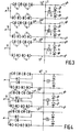
- Fig. 3 shows diagrammatically a first embodiment of a part of a display arrangement according to the invention, especially a part of the control section. As described above, each
picture element 12 forming part of, for example, a matrix is connected on the one hand via thepicture electrode 7 to acolumn electrode 11 and is connected on the other hand via thepicture electrode 6 and two diodes 9a and 9b or other unilaterally non-linear switching elements to tworow electrodes 8a, 8b. As already described in the introduction, such a circuit, in which the display arrangement is controlled according to the ac-D2C method, gives rise to doubling of the number of row connection points. In order to avoid this, according to the invention, the control lines 13 of therow electrodes 8a, 8b include a number of additional diodes 14a, 14b. Thesediodes diodes 9a and 9b, respectively. The two series arrangements are in turn connected in parallel between a (from a viewpoint of switching technique common)point 15 corresponding to thepicture electrode 6 and adriving point 16. - Although the
diodes 14 may be manufactured in a manner different from that in which thediodes 9 are manufactured, it is assumed hereinafter that thediodes - Let is be assumed that the number of diodes in the
selection lines 13a, 13b is equal and amounts to k. Upon selection, the voltage drop between thedriving point 16 and thejunction point 15 is then at least (k+1)VON. With a selected cell, a data voltage \VD\ is supplied at thecolumn electrode 11, where 0 ≤ VD ≤VDMAX, so that the voltage difference across thepicture element 12 is VD, and VON across the (k+1)diodes 14, 9 (k+1) VON' However, limitations are set to the data voltage because after one field period the picture element is generally operated with inverted voltages. The data voltage therefore has a value between -VDMAX an VDMAX'. Due to capacitive couplings between thepicture electrodes electrodes 6. In a frame period in which thepoint 16 is operated with negative voltages, a nonselected line receives a voltage O at thepoint 16. In order to avoid discharge of theelectrode 6, it is then required that VDMAX ≤(k+1)VOFF. A nonselected row which still has to be written receives at the point 16 a voltage (k+1)VOFF. With such a row, the maximum voltage at theelectrode 6 is 2VDMAX and the minimum voltage is 0 so that it holds again that VDMAX ≤ (k+1 )VOFF. - In a next field period in which the
point 16 is operated with positive voltages and the data voltages lie between -VDMAX and 0, these voltages change their signs. Consequently, it holds that \VD\≤ (k+1)VOFF. - As stated above, the maximum voltage across the picture element is VD with 0≤ VD ≤ (k+1)VOFF. With such an arrangement, a wide choice is thus possible especially in the kind of LCD liquid to be used, because by increase and decrease, respectively, of the number of
diodes 14 the maximum voltage to be used across thepicture element 12 is increased and decreased, respectively. - Although the arrangement shown consequently offers a wider choice in the optoelectronic material to be used, it is found that especially With larger matrices of picture elements, capacitive cross-talk has an unfavourable influence. This is especially the case with the use of a control method in which for the average voltage across a picture element a value Vc = VSAT +VTH (cf. Fig. 2) is chosen. In this method, the absolute value of the voltage across the
picture element 12 remains practically limited to the range between VTH and VSAT. This is described more fully in "A LCTV Display Controlled by a -Si Diode Rings" of S. Togashi et al in SID 84, Digest, p. 324-5. The said capacitive effect results in that under given conditions such signal variations can occur at the row electrodes that undesired charging or discharging via thediodes 14 can occur. - Fig. 4 shows diagramnatically a part of a control device in which this disadvantage is net by connecting a
diode 17 antiparallel to thediodes 14. When thediodes 14 are switched off, the row electrodes 8 now do not assume an undefined voltage value, but these electrodes 8 assume via the additional diodes 17 a voltage value which is higher or lower by an amount equal to the forward voltage of thediode 17 than the voltage at thepoint 16. - This current through the
diode 17 can be a few times larger than that through thediodes 14 so that other ON and OFF voltages hold for thediodes 17. For the sake of completeness, other ON and OFF voltages will be given also for thediodes 14 hereinafter. With the aforementioned control about VC and with ON and OFF voltages - VON and VOFF for the
diodes 9, - V' ON and V' OFF for the diodes 14 (k in number)
- V" ON and V" OFF for the
diodes 17, the following criteria are applied (Figures 2, 4):


- These criteria can be seen as follows. With a drive according to the method of Togashi et al, upon selection the
point 15 has to reach a voltage VC = ½(VSAT+ VTH). A satisfactory operation is attained if, dependent upon the information at thecolumn electrode 11, the capacitance constituted by the picture electrode is charged to VC + VDMAX = VSAT or to VC -VDMAX = VTHR. Elimination of VC from this relation gives \VD\MAX = ½(VSAT- VTH) (b). Upon selection of other picture elements, voltages between -VDMAX and +VDMAX can occur at thecolum electrode 11. Via capacitive coupling the maximum and minimum voltages at thejunction point 15 are then VMIN = -VDMAX -VSAT and VMAX=VDMAX-VTH, respectively. In case of non-selection, thejunction point 15 may then just not be charged and discharged, respectively, in other words VNONSEL-KVOFF= VMIN and VNONSEL-V"ON + VOFF = VMAX' respectively (1). - This gives


- Fig. 5 shows an embodiment in which the charging current and the discharging current of the capacitances associated with the
picture element 12 follow in part the same current path, i.e. a series arrangement of k diodes 14 (in this case k = 3). In a similar manner as for the configuration of Fig. 4, it can again be derived that the following criteria hold:


point 15 has to receive a voltage Vc = ½(VSAT + VTH), while also VC + V DMAX= VSAT and VC - VDMAX = VTH have to be satisfied again. It holds then again for thepoint 15 that

- In the case of non-selection, this
junction point 15 may not yet be charged and discharged, respectively, so that it holds that


- In this manner, the number of diodes in the peripheral electronic circuit can thus be considerably reduced (in the present example, whilst maintaining practically the same control voltage range across the picture element, the number of diodes is nearly halved with respect to the configuration of Fig. 4).
- Fig. 6 finally shows in plan view a possible embodiment of the
picture electrode 6, which is made, for example, of indium tin oxide. This electrode is connected through thediodes 9a, 9b shown diagranma- tically to the aluminium row electrodes 8a, 8b. Thediodes picture electrode 6 is obtained. In order to obtain an increased reliability, it is of course possible to subdivide thepicture electrode 6 into several sub- electrodes, which are each connected viaseparate diodes additional diodes - Of course the invention is not limited to the embodiments shown herein, but various modifications are possible within the scope of the invention. For example, in the configurations of Figures 4 and 5 diodes may be connected parallel to the
diodes 17 in order to increase the reliability in operation. Such a parallel arrangement then again fulfils the function of a unilaterally non-linear switching element. Furthermore, in the arrangement of Fig. 4, instead of onediode 17, two diodes may be connected in series, while the common point may be connected, if desired, to a point in the circuit of thediodes 14, which is thus connected antiparallel. Moreover, for example, the circuit of thediodes 14 in Fig. 5 may have a double construction. Besides in liquid crystal display arrangements, a switching matrix as described may also be used in other display media, such as, for example, electrophoretic and electrochrome display media.
Claims (7)
Applications Claiming Priority (2)
| Application Number | Priority Date | Filing Date | Title |
|---|---|---|---|
| NL8502662 | 1985-09-30 | ||
| NL8502662A NL8502662A (en) | 1985-09-30 | 1985-09-30 | DISPLAY DEVICE WITH IMPROVED CONTROL. |
Publications (2)
| Publication Number | Publication Date |
|---|---|
| EP0217469A1 true EP0217469A1 (en) | 1987-04-08 |
| EP0217469B1 EP0217469B1 (en) | 1990-12-27 |
Family
ID=19846640
Family Applications (1)
| Application Number | Title | Priority Date | Filing Date |
|---|---|---|---|
| EP86201660A Expired - Lifetime EP0217469B1 (en) | 1985-09-30 | 1986-09-24 | Display arrangement with improved drive |
Country Status (7)
| Country | Link |
|---|---|
| US (1) | US4794385A (en) |
| EP (1) | EP0217469B1 (en) |
| JP (1) | JPH0731484B2 (en) |
| KR (1) | KR940005236B1 (en) |
| CA (1) | CA1273138A (en) |
| DE (1) | DE3676614D1 (en) |
| NL (1) | NL8502662A (en) |
Cited By (4)
| Publication number | Priority date | Publication date | Assignee | Title |
|---|---|---|---|---|
| EP0296662A2 (en) * | 1987-06-18 | 1988-12-28 | Koninklijke Philips Electronics N.V. | Display device and method of driving such a device |
| EP0357147A1 (en) * | 1988-09-01 | 1990-03-07 | Koninklijke Philips Electronics N.V. | Display device |
| EP0362939A1 (en) * | 1988-10-05 | 1990-04-11 | Koninklijke Philips Electronics N.V. | Method of driving a display device |
| EP0430360A1 (en) * | 1989-11-27 | 1991-06-05 | Koninklijke Philips Electronics N.V. | Active display device |
Families Citing this family (9)
| Publication number | Priority date | Publication date | Assignee | Title |
|---|---|---|---|---|
| NL8701420A (en) * | 1987-06-18 | 1989-01-16 | Philips Nv | DISPLAY DEVICE AND METHOD FOR CONTROLLING SUCH DISPLAY DEVICE. |
| DE3888735T2 (en) * | 1987-06-18 | 1994-10-27 | Philips Nv | Display device. |
| GB2215506A (en) * | 1988-02-24 | 1989-09-20 | Philips Electronic Associated | Matrix display devices |
| GB2219682A (en) * | 1988-06-10 | 1989-12-13 | Philips Electronic Associated | Matrix display device |
| NL8802997A (en) * | 1988-12-07 | 1990-07-02 | Philips Nv | DISPLAY DEVICE. |
| DE69106302T2 (en) * | 1990-10-05 | 1995-05-18 | Toshiba Kawasaki Kk | Method and device for controlling a liquid crystal display device. |
| US5483085A (en) * | 1994-05-09 | 1996-01-09 | Motorola, Inc. | Electro-optic integrated circuit with diode decoder |
| WO2006085241A1 (en) * | 2005-02-14 | 2006-08-17 | Koninklijke Philips Electronics N.V. | Active matrix display devices |
| WO2007057811A1 (en) * | 2005-11-16 | 2007-05-24 | Polymer Vision Limited | Method for addressing active matrix displays with ferroelectrical thin film transistor based pixels |
Citations (1)
| Publication number | Priority date | Publication date | Assignee | Title |
|---|---|---|---|---|
| EP0070598A1 (en) * | 1981-07-16 | 1983-01-26 | Koninklijke Philips Electronics N.V. | Display device |
Family Cites Families (3)
| Publication number | Priority date | Publication date | Assignee | Title |
|---|---|---|---|---|
| US3654606A (en) * | 1969-11-06 | 1972-04-04 | Rca Corp | Alternating voltage excitation of liquid crystal display matrix |
| US4251136A (en) * | 1979-07-25 | 1981-02-17 | Northern Telecom Limited | LCDs (Liquid crystal displays) controlled by thin film diode switches |
| US4554537A (en) * | 1982-10-27 | 1985-11-19 | At&T Bell Laboratories | Gas plasma display |
-
1985
- 1985-09-30 NL NL8502662A patent/NL8502662A/en not_active Application Discontinuation
-
1986
- 1986-09-22 US US06/910,103 patent/US4794385A/en not_active Expired - Fee Related
- 1986-09-24 DE DE8686201660T patent/DE3676614D1/en not_active Expired - Lifetime
- 1986-09-24 EP EP86201660A patent/EP0217469B1/en not_active Expired - Lifetime
- 1986-09-30 KR KR1019860008208A patent/KR940005236B1/en not_active IP Right Cessation
- 1986-09-30 JP JP61233125A patent/JPH0731484B2/en not_active Expired - Lifetime
- 1986-10-15 CA CA000520563A patent/CA1273138A/en not_active Expired - Lifetime
Patent Citations (1)
| Publication number | Priority date | Publication date | Assignee | Title |
|---|---|---|---|---|
| EP0070598A1 (en) * | 1981-07-16 | 1983-01-26 | Koninklijke Philips Electronics N.V. | Display device |
Non-Patent Citations (1)
| Title |
|---|
| PROCEEDINGS OF THE IEEE, vol. 59, no. 11, November 1971, pages 1566-1579, New York, US; B.J.LECHNER et al.: "Liquid crystal matrix displays" * |
Cited By (5)
| Publication number | Priority date | Publication date | Assignee | Title |
|---|---|---|---|---|
| EP0296662A2 (en) * | 1987-06-18 | 1988-12-28 | Koninklijke Philips Electronics N.V. | Display device and method of driving such a device |
| EP0296662A3 (en) * | 1987-06-18 | 1989-01-11 | N.V. Philips' Gloeilampenfabrieken | Display device and method of driving such a device |
| EP0357147A1 (en) * | 1988-09-01 | 1990-03-07 | Koninklijke Philips Electronics N.V. | Display device |
| EP0362939A1 (en) * | 1988-10-05 | 1990-04-11 | Koninklijke Philips Electronics N.V. | Method of driving a display device |
| EP0430360A1 (en) * | 1989-11-27 | 1991-06-05 | Koninklijke Philips Electronics N.V. | Active display device |
Also Published As
| Publication number | Publication date |
|---|---|
| CA1273138A (en) | 1990-08-21 |
| JPH0731484B2 (en) | 1995-04-10 |
| KR940005236B1 (en) | 1994-06-15 |
| DE3676614D1 (en) | 1991-02-07 |
| JPS6290694A (en) | 1987-04-25 |
| NL8502662A (en) | 1987-04-16 |
| US4794385A (en) | 1988-12-27 |
| KR870003460A (en) | 1987-04-17 |
| EP0217469B1 (en) | 1990-12-27 |
Similar Documents
| Publication | Publication Date | Title |
|---|---|---|
| USRE37906E1 (en) | Display device and method of driving such a device | |
| EP0217466B1 (en) | Display arrangement with improved drive | |
| US6590552B1 (en) | Method of driving liquid crystal display device | |
| EP0489459B1 (en) | Method of driving a matrix display device and a matrix display device operable by such a method | |
| EP0217469B1 (en) | Display arrangement with improved drive | |
| EP0296663B1 (en) | Display device | |
| JP2529696B2 (en) | Display device | |
| US5032830A (en) | Electro-optical display device with non-linear switching units with auxiliary voltages and capacitively coupled row electrodes | |
| US5323254A (en) | Display device with electrostatic discharge protection | |
| US5576728A (en) | Driving method for an electrooptical device | |
| EP0296662B1 (en) | Display device and method of driving such a device | |
| EP0224388A2 (en) | Active matrix liquid crystal display device | |
| JPH0474716B2 (en) | ||
| WO2008085666A1 (en) | Active matrix with write memory | |
| JPH04225331A (en) | Active matrix liquid crystal display device | |
| JPH049920A (en) | Method for driving opto-electrical device | |
| JPH04261516A (en) | Method for driving liquid crystal display element | |
| JPH0718987B2 (en) | Display device |
Legal Events
| Date | Code | Title | Description |
|---|---|---|---|
| PUAI | Public reference made under article 153(3) epc to a published international application that has entered the european phase |
Free format text: ORIGINAL CODE: 0009012 |
|
| AK | Designated contracting states |
Kind code of ref document: A1 Designated state(s): CH DE FR GB LI NL |
|
| 17P | Request for examination filed |
Effective date: 19870716 |
|
| 17Q | First examination report despatched |
Effective date: 19890608 |
|
| GRAA | (expected) grant |
Free format text: ORIGINAL CODE: 0009210 |
|
| AK | Designated contracting states |
Kind code of ref document: B1 Designated state(s): CH DE FR GB LI NL |
|
| PG25 | Lapsed in a contracting state [announced via postgrant information from national office to epo] |
Ref country code: NL Effective date: 19901227 |
|
| REF | Corresponds to: |
Ref document number: 3676614 Country of ref document: DE Date of ref document: 19910207 |
|
| ET | Fr: translation filed | ||
| NLV1 | Nl: lapsed or annulled due to failure to fulfill the requirements of art. 29p and 29m of the patents act | ||
| PLBE | No opposition filed within time limit |
Free format text: ORIGINAL CODE: 0009261 |
|
| STAA | Information on the status of an ep patent application or granted ep patent |
Free format text: STATUS: NO OPPOSITION FILED WITHIN TIME LIMIT |
|
| PGFP | Annual fee paid to national office [announced via postgrant information from national office to epo] |
Ref country code: CH Payment date: 19911217 Year of fee payment: 6 |
|
| 26N | No opposition filed | ||
| PG25 | Lapsed in a contracting state [announced via postgrant information from national office to epo] |
Ref country code: LI Effective date: 19920930 Ref country code: CH Effective date: 19920930 |
|
| REG | Reference to a national code |
Ref country code: CH Ref legal event code: PL |
|
| REG | Reference to a national code |
Ref country code: FR Ref legal event code: CD |
|
| PGFP | Annual fee paid to national office [announced via postgrant information from national office to epo] |
Ref country code: GB Payment date: 19960830 Year of fee payment: 11 |
|
| PGFP | Annual fee paid to national office [announced via postgrant information from national office to epo] |
Ref country code: FR Payment date: 19960925 Year of fee payment: 11 |
|
| PGFP | Annual fee paid to national office [announced via postgrant information from national office to epo] |
Ref country code: DE Payment date: 19961125 Year of fee payment: 11 |
|
| PG25 | Lapsed in a contracting state [announced via postgrant information from national office to epo] |
Ref country code: GB Free format text: LAPSE BECAUSE OF NON-PAYMENT OF DUE FEES Effective date: 19970924 |
|
| PG25 | Lapsed in a contracting state [announced via postgrant information from national office to epo] |
Ref country code: FR Free format text: THE PATENT HAS BEEN ANNULLED BY A DECISION OF A NATIONAL AUTHORITY Effective date: 19970930 |
|
| GBPC | Gb: european patent ceased through non-payment of renewal fee |
Effective date: 19970924 |
|
| PG25 | Lapsed in a contracting state [announced via postgrant information from national office to epo] |
Ref country code: DE Free format text: LAPSE BECAUSE OF NON-PAYMENT OF DUE FEES Effective date: 19980603 |
|
| REG | Reference to a national code |
Ref country code: FR Ref legal event code: ST |