EP0070598A1 - Display device - Google Patents
Display device Download PDFInfo
- Publication number
- EP0070598A1 EP0070598A1 EP82200879A EP82200879A EP0070598A1 EP 0070598 A1 EP0070598 A1 EP 0070598A1 EP 82200879 A EP82200879 A EP 82200879A EP 82200879 A EP82200879 A EP 82200879A EP 0070598 A1 EP0070598 A1 EP 0070598A1
- Authority
- EP
- European Patent Office
- Prior art keywords
- picture
- display device
- conductivity type
- electrodes
- junctions
- Prior art date
- Legal status (The legal status is an assumption and is not a legal conclusion. Google has not performed a legal analysis and makes no representation as to the accuracy of the status listed.)
- Granted
Links
Images
Classifications
-
- G—PHYSICS
- G09—EDUCATION; CRYPTOGRAPHY; DISPLAY; ADVERTISING; SEALS
- G09G—ARRANGEMENTS OR CIRCUITS FOR CONTROL OF INDICATING DEVICES USING STATIC MEANS TO PRESENT VARIABLE INFORMATION
- G09G3/00—Control arrangements or circuits, of interest only in connection with visual indicators other than cathode-ray tubes
- G09G3/20—Control arrangements or circuits, of interest only in connection with visual indicators other than cathode-ray tubes for presentation of an assembly of a number of characters, e.g. a page, by composing the assembly by combination of individual elements arranged in a matrix no fixed position being assigned to or needed to be assigned to the individual characters or partial characters
- G09G3/34—Control arrangements or circuits, of interest only in connection with visual indicators other than cathode-ray tubes for presentation of an assembly of a number of characters, e.g. a page, by composing the assembly by combination of individual elements arranged in a matrix no fixed position being assigned to or needed to be assigned to the individual characters or partial characters by control of light from an independent source
- G09G3/36—Control arrangements or circuits, of interest only in connection with visual indicators other than cathode-ray tubes for presentation of an assembly of a number of characters, e.g. a page, by composing the assembly by combination of individual elements arranged in a matrix no fixed position being assigned to or needed to be assigned to the individual characters or partial characters by control of light from an independent source using liquid crystals
- G09G3/3611—Control of matrices with row and column drivers
- G09G3/367—Control of matrices with row and column drivers with a nonlinear element in series with the liquid crystal cell, e.g. a diode, or M.I.M. element
-
- G—PHYSICS
- G02—OPTICS
- G02F—OPTICAL DEVICES OR ARRANGEMENTS FOR THE CONTROL OF LIGHT BY MODIFICATION OF THE OPTICAL PROPERTIES OF THE MEDIA OF THE ELEMENTS INVOLVED THEREIN; NON-LINEAR OPTICS; FREQUENCY-CHANGING OF LIGHT; OPTICAL LOGIC ELEMENTS; OPTICAL ANALOGUE/DIGITAL CONVERTERS
- G02F1/00—Devices or arrangements for the control of the intensity, colour, phase, polarisation or direction of light arriving from an independent light source, e.g. switching, gating or modulating; Non-linear optics
- G02F1/01—Devices or arrangements for the control of the intensity, colour, phase, polarisation or direction of light arriving from an independent light source, e.g. switching, gating or modulating; Non-linear optics for the control of the intensity, phase, polarisation or colour
- G02F1/13—Devices or arrangements for the control of the intensity, colour, phase, polarisation or direction of light arriving from an independent light source, e.g. switching, gating or modulating; Non-linear optics for the control of the intensity, phase, polarisation or colour based on liquid crystals, e.g. single liquid crystal display cells
- G02F1/133—Constructional arrangements; Operation of liquid crystal cells; Circuit arrangements
- G02F1/136—Liquid crystal cells structurally associated with a semi-conducting layer or substrate, e.g. cells forming part of an integrated circuit
- G02F1/1362—Active matrix addressed cells
- G02F1/1365—Active matrix addressed cells in which the switching element is a two-electrode device
-
- H—ELECTRICITY
- H01—ELECTRIC ELEMENTS
- H01L—SEMICONDUCTOR DEVICES NOT COVERED BY CLASS H10
- H01L27/00—Devices consisting of a plurality of semiconductor or other solid-state components formed in or on a common substrate
- H01L27/02—Devices consisting of a plurality of semiconductor or other solid-state components formed in or on a common substrate including semiconductor components specially adapted for rectifying, oscillating, amplifying or switching and having at least one potential-jump barrier or surface barrier; including integrated passive circuit elements with at least one potential-jump barrier or surface barrier
- H01L27/04—Devices consisting of a plurality of semiconductor or other solid-state components formed in or on a common substrate including semiconductor components specially adapted for rectifying, oscillating, amplifying or switching and having at least one potential-jump barrier or surface barrier; including integrated passive circuit elements with at least one potential-jump barrier or surface barrier the substrate being a semiconductor body
- H01L27/08—Devices consisting of a plurality of semiconductor or other solid-state components formed in or on a common substrate including semiconductor components specially adapted for rectifying, oscillating, amplifying or switching and having at least one potential-jump barrier or surface barrier; including integrated passive circuit elements with at least one potential-jump barrier or surface barrier the substrate being a semiconductor body including only semiconductor components of a single kind
- H01L27/0814—Diodes only
Definitions
- the invention relates to a display device comprising an electro-optical display medium between two supporting plates, a system of picture elements arranged in rows and columns, in which each picture element is formed by two picture electrodes provided respectively on the facing surfaces of the supporting plates, a system of row and column electrodes for driving the picture elements, the row electrodes being provided on one supporting plate and the column electrodes being provided on the other supporting plate, and a system of switching elements in which a switching element is incorporated between a row electrode and a column electrode in series with each picture element, the said switching elements being formed by two series-arranged, oppositely directed diodes.
- Such a display medium is suitable for displaying alphanumerical information and video information by means of passive electro-optical display media, such as liquid crystals, electro- phoretic suspensions and electrochromic materials.
- the known passive electro-optical display media generally have an insufficiently steep threshold with respect to the applied voltage and/or have an insufficient intrinsic memory. In multiplexed matrix display devices these properties are the cause that the number of lines to be driven is small. Due to the lack of memory, the information presented to a selected row electrode via the column electrodes has to be written over and over again. Moreover, the voltages presented to the column electrodes are present not only across the picture elements of a driven row electrode, but also across the picture elements of all the other rows. As a result of this picture elements, during the time they are not driven, experience an effective voltage which may be sufficient to bring a picture element to the on-condition.
- the ratio of the effective voltage which a picture element experiences in the on and off-conditions, respectively decreases when the number of row electrodes increases. Due to the lack of a sufficiently steep threshold, the contrast between picture elements in the on- and off-condition decreases thereby.
- the number of rows to be driven may be increased by integrating an extra switch per picture.
- This switch ensures a sufficiently steep threshold with respect to the applied voltage and ensures that the information presented to a driven row electrode remains across a picture element during the time the remaining row electrodes are driven.
- the switch also prevents a picture element from experiencing an effective voltage during the time this is not driven.
- a display device of a kind mentioned in the opening paragraph is disclosed in United States Patent Specification 4,223,308.
- This known display device uses as switching elements two series-arranged, oppositely directed diodes (back-to-back diodes). These switching elements are symmetrical with respect to a voltage zero, which is desired because liquid crystal display devices are operated with alternating voltage to prevent degradation of the liquid crystal in the case of direct voltage control.
- One of the two back-to-back diodes is always in the reverse direction so that the threshold voltage is determined by the breakdown voltage of that diode.
- a display device of the kind mentioned in the opening paragraph is for that purpose characterized in that the said two diodes are formed by a semiconductor region of the first conductivity type which in two separate places forms a p-n junction with two respective semiconductor regions of the second conductivity type, the distance between the two p-n junctions being so small that in the operating condition punch-through occurs between the two p-n junctions before one of the two p-n junctions breaks down.
- the two diodes are integrated to form one assembly with a semiconductor region of the first conductivity type which is common to the two diodes.
- a depletion layer in which no free charge carriers are present is situated at the area of a p-n junction.
- the thickness of the common semiconductor region of the first conductivity type is chosen to be so small that before the reverse biased p-n junction breaks down the depletion layers in the common semiconductor region of the first conductivity type meet each other or overlap each other. As a result of this, punch-through occurs between the two semiconductor regions of the second conductivity type.
- the common semiconductor region of the first conductivity type obtains a negligibly small resistance.
- the series resistance across the switching element disappears so that a better switching ratio is obtained and a picture element can be driven with lower voltages than before.
- a first embodiment of a display device in accordance with the invention is characterized in that the two semiconductor regions of the second conductivity type are situated in the same plane as the semiconductor region of the first conductivity type.
- the switching elements are constructed as a completely flat structure. This embodiment has the advantage that symmetrical switching elements can be manufactured in this flat structure in a simple manner.
- a second embodiment in which the switching elements have a laminated structure is characterized in that the second semiconductor region of the second conductivity type is provided at least partly on the first semiconductor region on the second conductivity type, the said two regions being separated from each other by the semiconductor region of the first conductivity type.
- This embodiment has the advantage that very small distances can be realized between the two semiconductor regions of the second conductivity type.
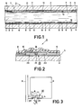
- Figure 1 is a sectional view of a part of a display device 1 having two supporting plates 2 and 3 between which a liquid crystal 4 is present.
- the inner surfaces of the supporting plates 2 and 3 have electrically and chemically insulating layers 5.
- a large number of picture electrodes 6 and 7 arranged respectively in rows and columns are provided on the supporting plates 2 and 3, respectively.
- the oppositely located picture electrodes 6 and 7 form the picture elements of the display device.
- Strip-shaped column electrodes 11 are provided between the columns of picture electrodes 7.
- the column electrodes 11 and the picture electrodes 7 can advantageously be integrated to strip-shaped electrodes.
- Strip-shaped row electrodes 8 are provided between the rows of picture electrodes 6.
- Each picture electrode 6 is connected to a row electrode 8 by means of a switching element 9 shown diagrammatically.
- the switching elements 9 give the liquid crystal 4 a sufficiently steep threshold with respect to the applied voltage and give the liquid crystal 4 a memory.
- Liquid crystal-orienting layers 10 are furthermore provided on the inner surfaces of the supporting plates 2 and 3. As is known, another orientation condition of the liquid crystal molecules and therewith an optically different condition can be obtained by applying a voltage across the liquid crystal layer 4.
- the display device can be realized both as a transmissive and as a reflective device.
- FIG 2 is a sectional view of a first embodiment of the switching elements 9 shown diagrammatically in Figure 1, in which like components are referred to by like reference numerals.
- a 0,2/um thick electrically and chemically insulating layer 5 of silicon nitride is provided on the supporting plate 2.
- a 1 ⁇ m thick layer of preferably already p-doped polysilicon is then provided on the layer 5, in which former layer polysilicon islands 20 are formed by means of a photolithographic process. If the starting material is undoped polysilicon, a p-doping is provided in the islands, for example by ion implantation of boron, to give an active doping concentration of 1 x 10 15 /cm 3 .
- a mask is provided on the polysilicon islands 20 by means of a photolithographic process for providing in the regions 22 and 23 and n + doping, for example by ion implantation of phosphorus, to give an active doping concentration of 1 x 10 18 /cm 3 .
- n + doping By providing the n + doping, a flat n + -pn + structure is formed in the islands 20.
- the assembly is then annealed for 1 hour at a maximum temperature of 1,000°C.
- a 0,2 ⁇ m thick covering layer 24 of silicon oxide or silicon nitride is then provided over the p-doped region 21 and partly over the n +- doped regions 22 and 23.
- the picture electrodes 6 and the row electrodes 8 of indium oxide and/or tin oxide are then provided in a thickness of 0.15 ⁇ m in such manner that a picture electrode 6 covers the exposed surface of the n+-doped region 22 and a raw electrode 8 covers the exposed surface of the n + -doped region 23.
- a 0.1 ⁇ m thick orienting layer 10 of a polyimide is then provided over the whole structure.
- Figure 3 is a plan view of the structure shown in Figure 2.
- the surface area of the picture electrodes is approximately 250 x 250 ⁇ m 2 .
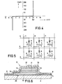
- Figure 4 shows the current voltage characteristic of the described switching element with the said doping concentrations.
- V pt the voltage V is substantially independent of the current I, so that the series resistance of the switching element is negligibly small. This is the result of the very small width d of the p-doped region 21.
- the depletion layer of the reverse biased p-n junction expands to a greater extent in the region 21 than the depletion layer of the forward biased p-n junction decreases in the region.
- the two depletion layers melt each other and overlap each other, respectively, before breakdown occurs.
- the characteristic is completely symmetrical, which is desirable because the display device is operated with alternating voltage so as to prevent undesired electrode processes by direct voltage drive.
- the value of the punch-through voltage V pt which is independent of the dimensions a and b of the switching element, can be adjusted by means of the doping concentrations and the width d of the region 21. The occurring reverse current can be minimized by suitable choice of the width b and the thickness of the switching elements.
- the driving of the display device will be described in greater detail with reference to Figure 5.
- the picture elements formed by the picture electrodes 6 and 7 are connected between the row electrodes 8 and the column electrodes 11, a switching element 9 being connected in series with each picture element.
- the row electrodes 8 are driven by voltage pulses +V s .
- voltage pulses -V d are applied to selected column electrodes 11.
- a voltage difference V s +V d then exists across said selected column electrodes 11 and the associated raw electrode 8. This voltage difference also exists across the series arrangement of the picture elements and the switching elements 9.
- the voltage difference V s +V d is larger than the threshold voltage Vpt of the switching elements 9.
- V s + V d As a result of this a part of the voltage difference V s + V d comes across the driven picture elements, which is sufficient to bring the liquid crystal 4 at the area of the picture elements to a different orientation condition.
- Voltage pulses +V d are applied to the non- selected column electrodes 11. A voltage difference V s - V d then exists across said column electrodes 11 and the row electrodes 8. This voltage difference Vs - V d is smaller than the threshold voltage V pt of the switching elements so that they are not energized.
- the voltage pulses ⁇ V d are smaller than the threshold voltage V pt of the switching elements 9. This prevents information being written in picture elements of non-driven row electrodes 8. After the information has been written on a driven row electrode 8, the next row electrode 8 is energized.
- both the row electrodes and column electrodes may serve as control electrodes or information electrodes.
- Figure 6 shows a second embodiment of the switching elements 9 shown diagrammatically in Figure 1.
- Like components are referred to by like reference numerals as in Figure 1.
- a 0.2 ⁇ m thick electrically and chemically insulating layer 5 of silicon nitride is provided on the supporting plate 2.
- a 1 ⁇ m thick n + doped layer 30 of polysilicon, a 0.1 to 1 ⁇ m thick p-doped layer 31 of polysilicon and again a 1 ⁇ m thick n + -doped layer 32 of polysilicon are provided successively on the layer 5 by means of chemical vapour-deposition methods.
- the doping concentrations are in the same order of magnitude as in the embodiment described with reference to Figure 2.
- a 0,1 ⁇ m thick covering layer (capping layer) of undoped polysilicon may be provided between the two n + -p junctions.
- a photolithographic process polysilicon islands 20 are formed.
- a mask is then provided photolithographically so as to etch away a part of the polysilicon island 20 and to thus create a contact possibility with the n + -doped layer 30.
- a 0.2 ⁇ m thick capping layer 34 of silicon oxide or silicon nitride is then provided over the whole island 20.
- Contact holes are etched herein photolithographically for the 0.15 ⁇ m thick picture electrodes 6 and row electrodes 8 of indium oxide and/or tin oxide to be provided afterwards, in such manner that the picture electrode 6 covers the exposed surface of the n + -doped region 32 and the row electrode 8 covers the exposed surface of the n + -doped region 30.
- a 0.1 / um thick liquid crystal-orienting layer 35 of a polymer is then provided over the whole structure.
- the stacked n + p-n + structure can also be realized by successively implanting a 2/um thick undoped layer of polysilicon with, for example, phosphorus, boron, and again phosphorus with such an energy that the concentration maxima are sufficiently spaced to form separated n + , p and n + doped regions.
- the switching elements may also be constructed in a p-n-p structure.
- the switching elements may also be used with other display media showing substantially no threshold and/or no intrinsic memory, for example, electrophoretic and electroceramic display media.
Abstract
Description
- The invention relates to a display device comprising an electro-optical display medium between two supporting plates, a system of picture elements arranged in rows and columns, in which each picture element is formed by two picture electrodes provided respectively on the facing surfaces of the supporting plates, a system of row and column electrodes for driving the picture elements, the row electrodes being provided on one supporting plate and the column electrodes being provided on the other supporting plate, and a system of switching elements in which a switching element is incorporated between a row electrode and a column electrode in series with each picture element, the said switching elements being formed by two series-arranged, oppositely directed diodes.
- Such a display medium is suitable for displaying alphanumerical information and video information by means of passive electro-optical display media, such as liquid crystals, electro- phoretic suspensions and electrochromic materials.
- The known passive electro-optical display media generally have an insufficiently steep threshold with respect to the applied voltage and/or have an insufficient intrinsic memory. In multiplexed matrix display devices these properties are the cause that the number of lines to be driven is small. Due to the lack of memory, the information presented to a selected row electrode via the column electrodes has to be written over and over again. Moreover, the voltages presented to the column electrodes are present not only across the picture elements of a driven row electrode, but also across the picture elements of all the other rows. As a result of this picture elements, during the time they are not driven, experience an effective voltage which may be sufficient to bring a picture element to the on-condition. Furthermore, the ratio of the effective voltage which a picture element experiences in the on and off-conditions, respectively, decreases when the number of row electrodes increases. Due to the lack of a sufficiently steep threshold, the contrast between picture elements in the on- and off-condition decreases thereby.
- It is known that the number of rows to be driven may be increased by integrating an extra switch per picture. This switch ensures a sufficiently steep threshold with respect to the applied voltage and ensures that the information presented to a driven row electrode remains across a picture element during the time the remaining row electrodes are driven. The switch also prevents a picture element from experiencing an effective voltage during the time this is not driven.
- A display device of a kind mentioned in the opening paragraph is disclosed in United States Patent Specification 4,223,308. This known display device uses as switching elements two series-arranged, oppositely directed diodes (back-to-back diodes). These switching elements are symmetrical with respect to a voltage zero, which is desired because liquid crystal display devices are operated with alternating voltage to prevent degradation of the liquid crystal in the case of direct voltage control. One of the two back-to-back diodes is always in the reverse direction so that the threshold voltage is determined by the breakdown voltage of that diode.
- These known back-to-back diodes are formed by two p-n-junctions which are interconnected by means of a conductor. Hoover, this structure has the disadvantage that the p-n structures have a voltage-dependent series resistance which is particularly large when one of the regions of the p-n structures is lightly doped, notably in amorphous and polycrystalline semiconductor materials. This means that upon energizing a picture element at the threshold voltage of the electro-optical effect, the voltage drop across the series resistance of the switching element has to be added in addition to the threshold voltage of the switching element, so that the resistance in the on-condition is unfavourably influenced and an unfavourable switching ratio is obtained. The switching ratio is the ratio between the resistance of the switching element in the on- and offstate.
- It is therefore the object of the invention to provide a switching element with which a better switching ratio is obtained and with which lower voltages for driving the display device are possible.
- A display device of the kind mentioned in the opening paragraph is for that purpose characterized in that the said two diodes are formed by a semiconductor region of the first conductivity type which in two separate places forms a p-n junction with two respective semiconductor regions of the second conductivity type, the distance between the two p-n junctions being so small that in the operating condition punch-through occurs between the two p-n junctions before one of the two p-n junctions breaks down. In a switching element according to the invention the two diodes are integrated to form one assembly with a semiconductor region of the first conductivity type which is common to the two diodes. As is known, a depletion layer in which no free charge carriers are present is situated at the area of a p-n junction. Hence two depletion layers extend in the common semiconductor region of the first conductivity type. When a voltage is applied across the two diodes, the width of the depletion layer of the reverse-biased p-n junction increases to a greater extent when the voltage increases than the width of the depletion layer of the forward-biased p-n junction decreases. According to the invention, the thickness of the common semiconductor region of the first conductivity type is chosen to be so small that before the reverse biased p-n junction breaks down the depletion layers in the common semiconductor region of the first conductivity type meet each other or overlap each other. As a result of this, punch-through occurs between the two semiconductor regions of the second conductivity type. As a result of the punch-through effect, the common semiconductor region of the first conductivity type obtains a negligibly small resistance. As a result of this construction of the diodes, the series resistance across the switching element disappears so that a better switching ratio is obtained and a picture element can be driven with lower voltages than before.
- It is to be noted that punch-through effects in series-arranged and oppositely arranged p-n junctions are known per se from Netherlands Patent Application 7801532 which relates to a ROM (read-only memory). However, this does not include the use as a switching element in a passive electro-optical display device.
- A first embodiment of a display device in accordance with the invention is characterized in that the two semiconductor regions of the second conductivity type are situated in the same plane as the semiconductor region of the first conductivity type. The switching elements are constructed as a completely flat structure. This embodiment has the advantage that symmetrical switching elements can be manufactured in this flat structure in a simple manner.
- A second embodiment in which the switching elements have a laminated structure is characterized in that the second semiconductor region of the second conductivity type is provided at least partly on the first semiconductor region on the second conductivity type, the said two regions being separated from each other by the semiconductor region of the first conductivity type. This embodiment has the advantage that very small distances can be realized between the two semiconductor regions of the second conductivity type.
- Embodiments of the invention will now be described by way of example, with reference to the accompanying drawing, in which:
- Figure 1 is a diagrammatic sectional view of a part of a display device of the type to which the invention relates;
- Figure 2 is a sectional view of a first embodiment of a switching element for the display device shown in Figure 1;
- Figure 3 is a plan view of the structure shown in Figure 2;
- Figure 4 shows a voltage-current characteristic of the switching element shown in Figures 2 and 3;
- Figure 5 shows the driving diagram of the display device shown in Figure 1;
- Figure 6 is a sectional view of a second embodiment of a switching element for the display device shown in Figure 1.
- Figure 1 is a sectional view of a part of a
display device 1 having two supportingplates liquid crystal 4 is present. The inner surfaces of the supportingplates layers 5. A large number ofpicture electrodes plates picture electrodes shaped column electrodes 11 are provided between the columns ofpicture electrodes 7. Thecolumn electrodes 11 and thepicture electrodes 7 can advantageously be integrated to strip-shaped electrodes. Strip-shaped row electrodes 8 are provided between the rows ofpicture electrodes 6. Eachpicture electrode 6 is connected to arow electrode 8 by means of aswitching element 9 shown diagrammatically. Theswitching elements 9 give the liquid crystal 4 a sufficiently steep threshold with respect to the applied voltage and give the liquid crystal 4 a memory. Liquid crystal-orienting layers 10 are furthermore provided on the inner surfaces of the supportingplates liquid crystal layer 4. The display device can be realized both as a transmissive and as a reflective device. - Figure 2 is a sectional view of a first embodiment of the
switching elements 9 shown diagrammatically in Figure 1, in which like components are referred to by like reference numerals. A 0,2/um thick electrically and chemically insulatinglayer 5 of silicon nitride is provided on the supportingplate 2. A 1µm thick layer of preferably already p-doped polysilicon is then provided on thelayer 5, in which formerlayer polysilicon islands 20 are formed by means of a photolithographic process. If the starting material is undoped polysilicon, a p-doping is provided in the islands, for example by ion implantation of boron, to give an active doping concentration of 1 x 10¹⁵/cm3. A mask is provided on thepolysilicon islands 20 by means of a photolithographic process for providing in theregions islands 20. The assembly is then annealed for 1 hour at a maximum temperature of 1,000°C. A 0,2µm thick coveringlayer 24 of silicon oxide or silicon nitride is then provided over the p-dopedregion 21 and partly over the n+-dopedregions picture electrodes 6 and therow electrodes 8 of indium oxide and/or tin oxide are then provided in a thickness of 0.15µm in such manner that apicture electrode 6 covers the exposed surface of the n+-doped region 22 and araw electrode 8 covers the exposed surface of the n+-dopedregion 23. A 0.1µmthick orienting layer 10 of a polyimide is then provided over the whole structure. - Figure 3 is a plan view of the structure shown in Figure 2. The surface area of the picture electrodes is approximately 250 x 250 µm2. The
polysilicon islands 20 have a length a = 50µm and a width b = 20µm. The islands occupy only a very small area with respect to the area of thepicture electrodes 6 so that theislands 20 are substantial unnoticable in the observed picture. The distance between the connections of thepicture electrodes 6 and therow electrodes 8 is c = 20µm. The width of the p-dopedregion 21 is d = 1/um. - Figure 4 shows the current voltage characteristic of the described switching element with the said doping concentrations. The punch-through or threshold voltage of the switching element is V pt = 6 V. Above Vpt the voltage V is substantially independent of the current I, so that the series resistance of the switching element is negligibly small. This is the result of the very small width d of the p-doped
region 21. Under the influence of the applied voltage, the depletion layer of the reverse biased p-n junction expands to a greater extent in theregion 21 than the depletion layer of the forward biased p-n junction decreases in the region. As a result of the small width d of theregion 21, the two depletion layers melt each other and overlap each other, respectively, before breakdown occurs. As a result of this, punch-through occurs between the two p-regions regions region 21. The occurring reverse current can be minimized by suitable choice of the width b and the thickness of the switching elements. - The driving of the display device will be described in greater detail with reference to Figure 5. The picture elements formed by the
picture electrodes row electrodes 8 and thecolumn electrodes 11, aswitching element 9 being connected in series with each picture element. Upon driving the display device, successively therow electrodes 8 are driven by voltage pulses +Vs. During the time araw electrode 8 is energized, voltage pulses -Vd are applied to selectedcolumn electrodes 11. A voltage difference Vs+Vd then exists across said selectedcolumn electrodes 11 and the associatedraw electrode 8. This voltage difference also exists across the series arrangement of the picture elements and theswitching elements 9. The voltage difference Vs+Vd is larger than the threshold voltage Vpt of theswitching elements 9. As a result of this a part of the voltage difference Vs + Vd comes across the driven picture elements, which is sufficient to bring theliquid crystal 4 at the area of the picture elements to a different orientation condition. Voltage pulses +Vd are applied to the non- selectedcolumn electrodes 11. A voltage difference Vs - Vd then exists across saidcolumn electrodes 11 and therow electrodes 8. This voltage difference Vs - Vd is smaller than the threshold voltage Vpt of the switching elements so that they are not energized. The voltage pulses ±Vd are smaller than the threshold voltage Vpt of theswitching elements 9. This prevents information being written in picture elements ofnon-driven row electrodes 8. After the information has been written on a drivenrow electrode 8, thenext row electrode 8 is energized. As a result of this, the voltage across theswitching elements 9 of therow electrode 8 driven earlier becomes smaller than the threshold voltage Vpt of the switching elements, so that one of the p-n junctions is reverse-biased and the written information cannot leak away directly via theswitching elements 9. This results in a long retention tine which is determined by the reverse current of theswitching elements 9. As a result of the long retention time it is possible to successively drive a very large number of rows and to provide them with information It is to be noted that both the row electrodes and column electrodes may serve as control electrodes or information electrodes. - Figure 6 shows a second embodiment of the
switching elements 9 shown diagrammatically in Figure 1. Like components are referred to by like reference numerals as in Figure 1. First, a 0.2µm thick electrically and chemically insulatinglayer 5 of silicon nitride is provided on the supportingplate 2. A 1µm thick n+ doped layer 30 of polysilicon, a 0.1 to 1µm thick p-dopedlayer 31 of polysilicon and again a 1µm thick n+-dopedlayer 32 of polysilicon are provided successively on thelayer 5 by means of chemical vapour-deposition methods. The doping concentrations are in the same order of magnitude as in the embodiment described with reference to Figure 2. If desired, a 0,1µm thick covering layer (capping layer) of undoped polysilicon may be provided between the two n+-p junctions. By means of a photolithographic process,polysilicon islands 20 are formed. A mask is then provided photolithographically so as to etch away a part of thepolysilicon island 20 and to thus create a contact possibility with the n+-doped layer 30. A 0.2µmthick capping layer 34 of silicon oxide or silicon nitride is then provided over thewhole island 20. Contact holes are etched herein photolithographically for the 0.15µmthick picture electrodes 6 androw electrodes 8 of indium oxide and/or tin oxide to be provided afterwards, in such manner that thepicture electrode 6 covers the exposed surface of the n+-dopedregion 32 and therow electrode 8 covers the exposed surface of the n+-doped region 30. A 0.1/um thick liquid crystal-orientinglayer 35 of a polymer is then provided over the whole structure. - It is to be noted that the stacked n+p-n+ structure can also be realized by successively implanting a 2/um thick undoped layer of polysilicon with, for example, phosphorus, boron, and again phosphorus with such an energy that the concentration maxima are sufficiently spaced to form separated n+, p and n+ doped regions.
- It will be obvious that the invention is not restricted to the above-described embodiments. In addition to the n-p-n structures shown, the switching elements may also be constructed in a p-n-p structure. Besides liquid crystal display devices, the switching elements may also be used with other display media showing substantially no threshold and/or no intrinsic memory, for example, electrophoretic and electroceramic display media.
Claims (6)
Applications Claiming Priority (2)
| Application Number | Priority Date | Filing Date | Title |
|---|---|---|---|
| NL8103376A NL8103376A (en) | 1981-07-16 | 1981-07-16 | DISPLAY DEVICE. |
| NL8103376 | 1981-07-16 |
Publications (2)
| Publication Number | Publication Date |
|---|---|
| EP0070598A1 true EP0070598A1 (en) | 1983-01-26 |
| EP0070598B1 EP0070598B1 (en) | 1987-01-14 |
Family
ID=19837794
Family Applications (1)
| Application Number | Title | Priority Date | Filing Date |
|---|---|---|---|
| EP82200879A Expired EP0070598B1 (en) | 1981-07-16 | 1982-07-12 | Display device |
Country Status (8)
| Country | Link |
|---|---|
| US (1) | US4583087A (en) |
| EP (1) | EP0070598B1 (en) |
| JP (1) | JPS5818674A (en) |
| CA (1) | CA1181513A (en) |
| DE (1) | DE3275142D1 (en) |
| ES (1) | ES513951A0 (en) |
| HK (1) | HK58288A (en) |
| NL (1) | NL8103376A (en) |
Cited By (18)
| Publication number | Priority date | Publication date | Assignee | Title |
|---|---|---|---|---|
| FR2551902A1 (en) * | 1983-09-13 | 1985-03-15 | Thomson Csf | NON-LINEAR ELEMENT ADDRESSING DISPLAY SCREEN AND METHOD FOR MANUFACTURING THE SAME |
| FR2553218A1 (en) * | 1983-10-07 | 1985-04-12 | Commissariat Energie Atomique | ACTIVE MATRIX DISPLAY SCREEN WITHOUT CROSSING LINES AND ADDRESSING COLUMNS |
| EP0150728A2 (en) * | 1984-01-23 | 1985-08-07 | Energy Conversion Devices, Inc. | Liquid crystal displays operated by amorphous silicon alloy diodes |
| EP0166225A2 (en) * | 1984-06-29 | 1986-01-02 | Energy Conversion Devices, Inc. | High yield liquid crystal display and method of making same |
| EP0174431A1 (en) * | 1984-09-10 | 1986-03-19 | International Business Machines Corporation | Liquid crystal display devices and method for production thereof |
| EP0184341A2 (en) * | 1984-11-12 | 1986-06-11 | Semiconductor Energy Laboratory Co., Ltd. | Liquid crystal display panel and manufacturing method thereof |
| FR2579775A1 (en) * | 1985-04-02 | 1986-10-03 | Thomson Csf | METHOD FOR PRODUCING NON-LINEAR CONTROL ELEMENTS FOR ELECTRO-OPTICAL VISUALIZATION DISPLAY SCREEN AND FLAT SCREEN CARRIED OUT ACCORDING TO THIS METHOD |
| EP0198346A2 (en) * | 1985-04-08 | 1986-10-22 | Energy Conversion Devices, Inc. | Solid-state threshold devices using punch-through |
| GB2173935A (en) * | 1985-04-03 | 1986-10-22 | Gen Electric Plc | Liquid crystal displays |
| FR2581781A1 (en) * | 1985-05-07 | 1986-11-14 | Thomson Csf | NON-LINEAR CONTROL ELEMENTS FOR ELECTROOPTIC DISPLAY SCREEN DISPLAY AND METHOD FOR MANUFACTURING THE SAME |
| EP0217469A1 (en) * | 1985-09-30 | 1987-04-08 | Koninklijke Philips Electronics N.V. | Display arrangement with improved drive |
| EP0217466A1 (en) * | 1985-09-30 | 1987-04-08 | Koninklijke Philips Electronics N.V. | Display arrangement with improved drive |
| EP0223967A1 (en) * | 1985-10-31 | 1987-06-03 | International Business Machines Corporation | Thin-film transistor liquid-crystal matrix display |
| EP0289071A1 (en) * | 1987-04-16 | 1988-11-02 | Philips Electronics Uk Limited | Liquid crystal display device |
| WO1989002095A1 (en) * | 1987-08-27 | 1989-03-09 | Hughes Aircraft Company | Lcmos displays fabricated with implant treated silicon wafers |
| US4839707A (en) * | 1987-08-27 | 1989-06-13 | Hughes Aircraft Company | LCMOS displays fabricated with implant treated silicon wafers |
| US4929569A (en) * | 1984-01-23 | 1990-05-29 | Ovonic Imaging Systems, Inc. | Method of fabricating amorphous silican diode addressed liquid crystal display |
| US5061040A (en) * | 1984-01-23 | 1991-10-29 | Ois Optical Imaging Systems, Inc. | Liquid crystal displays operated by amorphous silicon alloy diodes |
Families Citing this family (18)
| Publication number | Priority date | Publication date | Assignee | Title |
|---|---|---|---|---|
| JPH0617957B2 (en) * | 1985-05-15 | 1994-03-09 | セイコー電子工業株式会社 | Liquid crystal display |
| NL8601373A (en) * | 1986-05-29 | 1987-12-16 | Philips Nv | DISPLAY DEVICE WITH IMPROVED CONTROL. |
| JP2816549B2 (en) * | 1986-10-22 | 1998-10-27 | セイコーインスツルメンツ株式会社 | Electro-optical device |
| NL8701420A (en) * | 1987-06-18 | 1989-01-16 | Philips Nv | DISPLAY DEVICE AND METHOD FOR CONTROLLING SUCH DISPLAY DEVICE. |
| NL8702494A (en) * | 1987-10-19 | 1989-05-16 | Vermeulen Hollandia Octrooien | Swaying device. |
| GB2214018A (en) * | 1987-12-23 | 1989-08-23 | Philips Electronic Associated | Current mirror circuit arrangement |
| EP0322860B1 (en) * | 1987-12-28 | 1996-09-11 | Fuji Electric Co., Ltd. | Insulated gate semiconductor device |
| NL8802409A (en) * | 1988-09-30 | 1990-04-17 | Philips Nv | DISPLAY DEVICE, SUPPORT PLATE PROVIDED WITH DIODE AND SUITABLE FOR THE DISPLAY DEVICE AND METHOD FOR MANUFACTURING THE SUPPORT PLATE. |
| NL8802436A (en) * | 1988-10-05 | 1990-05-01 | Philips Electronics Nv | METHOD FOR CONTROLLING A DISPLAY DEVICE |
| NL8802997A (en) * | 1988-12-07 | 1990-07-02 | Philips Nv | DISPLAY DEVICE. |
| US5243452A (en) * | 1991-12-06 | 1993-09-07 | Ncr Corporation | Liquid crystal display with pen-input capability |
| US5751453A (en) * | 1991-12-06 | 1998-05-12 | Ncr Corporation | Liquid crystal display with pen-input capability |
| US5610629A (en) * | 1991-12-06 | 1997-03-11 | Ncr Corporation | Pen input to liquid crystal display |
| US5402145A (en) * | 1993-02-17 | 1995-03-28 | Copytele, Inc. | Electrophoretic display panel with arc driven individual pixels |
| JPH07152049A (en) * | 1993-11-29 | 1995-06-16 | Sharp Corp | Liquid crystal display device and its production |
| DE10328377A1 (en) * | 2003-06-24 | 2005-01-20 | Siemens Ag | Electrochromic display system |
| KR20070028604A (en) * | 2004-06-30 | 2007-03-12 | 코닌클리즈케 필립스 일렉트로닉스 엔.브이. | Method for manufacturing an electric device with a layer of conductive material contacted by nanowire |
| US20160313577A1 (en) * | 2015-04-23 | 2016-10-27 | Laxense Inc. | Dual-junction optical modulator and the method to make the same |
Citations (1)
| Publication number | Priority date | Publication date | Assignee | Title |
|---|---|---|---|---|
| US4223308A (en) * | 1979-07-25 | 1980-09-16 | Northern Telecom Limited | LCDs (Liquid crystal displays) controlled by thin film diode switches |
Family Cites Families (13)
| Publication number | Priority date | Publication date | Assignee | Title |
|---|---|---|---|---|
| JPS5135298A (en) * | 1974-09-20 | 1976-03-25 | Hitachi Ltd | EKISHOHYOJISOCHI |
| GB1573309A (en) * | 1976-03-24 | 1980-08-20 | Mullard Ltd | Semiconductor devices and their manufacture |
| GB1602361A (en) * | 1977-02-21 | 1981-11-11 | Zaidan Hojin Handotai Kenkyu | Semiconductor memory devices |
| JPS53145578A (en) * | 1977-05-25 | 1978-12-18 | Nec Corp | Diode varister |
| NL7801532A (en) * | 1978-02-10 | 1979-08-14 | Philips Nv | SEMI-GUIDE DEVICE. |
| JPS5559432A (en) * | 1978-10-27 | 1980-05-02 | Dainippon Printing Co Ltd | Electro-optical display panel of matrix type and device thereof |
| US4247915A (en) * | 1979-01-02 | 1981-01-27 | Texas Instruments Incorporated | Punch-through load devices in high density static memory cell |
| US4251136A (en) * | 1979-07-25 | 1981-02-17 | Northern Telecom Limited | LCDs (Liquid crystal displays) controlled by thin film diode switches |
| US4373165A (en) * | 1979-11-07 | 1983-02-08 | Texas Instruments Incorporated | Very high density punch-through read-only-memory |
| JPS5672488A (en) * | 1979-11-19 | 1981-06-16 | Matsushita Electric Ind Co Ltd | Liquid crystal display unit |
| US4405933A (en) * | 1981-02-04 | 1983-09-20 | Rca Corporation | Protective integrated circuit device utilizing back-to-back zener diodes |
| JPS57130081A (en) * | 1981-02-06 | 1982-08-12 | Matsushita Electric Ind Co Ltd | Liquid crystal picture display device |
| JPS57190923A (en) * | 1981-05-20 | 1982-11-24 | Seiko Epson Corp | Color liquid crystal display body |
-
1981
- 1981-07-16 NL NL8103376A patent/NL8103376A/en not_active Application Discontinuation
-
1982
- 1982-07-09 US US06/396,989 patent/US4583087A/en not_active Expired - Fee Related
- 1982-07-12 DE DE8282200879T patent/DE3275142D1/en not_active Expired
- 1982-07-12 EP EP82200879A patent/EP0070598B1/en not_active Expired
- 1982-07-14 ES ES513951A patent/ES513951A0/en active Granted
- 1982-07-14 JP JP57121363A patent/JPS5818674A/en active Pending
- 1982-07-15 CA CA000407376A patent/CA1181513A/en not_active Expired
-
1988
- 1988-08-04 HK HK582/88A patent/HK58288A/en unknown
Patent Citations (1)
| Publication number | Priority date | Publication date | Assignee | Title |
|---|---|---|---|---|
| US4223308A (en) * | 1979-07-25 | 1980-09-16 | Northern Telecom Limited | LCDs (Liquid crystal displays) controlled by thin film diode switches |
Non-Patent Citations (1)
| Title |
|---|
| NEUES AUS DER TECHNIK, no. 3, 15th June 1981, pages 2,3, Würzburg, (DE) * |
Cited By (31)
| Publication number | Priority date | Publication date | Assignee | Title |
|---|---|---|---|---|
| FR2551902A1 (en) * | 1983-09-13 | 1985-03-15 | Thomson Csf | NON-LINEAR ELEMENT ADDRESSING DISPLAY SCREEN AND METHOD FOR MANUFACTURING THE SAME |
| GB2146827A (en) * | 1983-09-13 | 1985-04-24 | Thomson Csf | Display panels |
| FR2553218A1 (en) * | 1983-10-07 | 1985-04-12 | Commissariat Energie Atomique | ACTIVE MATRIX DISPLAY SCREEN WITHOUT CROSSING LINES AND ADDRESSING COLUMNS |
| EP0145520A2 (en) * | 1983-10-07 | 1985-06-19 | Commissariat A L'energie Atomique | Display screen with active matrix without intersection of the row and column address lines |
| EP0145520A3 (en) * | 1983-10-07 | 1985-07-10 | Commissariat A L'energie Atomique Etablissement De Caractere Scientifique Technique Et Industriel | Display screen with active matrix without intersection of the row and column address lines |
| US4694287A (en) * | 1983-10-07 | 1987-09-15 | Commissariat A L'energie Atomique | Active matrix display screen without intersection of the addressing columns and rows |
| US4929569A (en) * | 1984-01-23 | 1990-05-29 | Ovonic Imaging Systems, Inc. | Method of fabricating amorphous silican diode addressed liquid crystal display |
| EP0150728A3 (en) * | 1984-01-23 | 1986-01-08 | Energy Conversion Devices, Inc. | Liquid crystal displays operated by amorphous silicon alloy diodes |
| US5061040A (en) * | 1984-01-23 | 1991-10-29 | Ois Optical Imaging Systems, Inc. | Liquid crystal displays operated by amorphous silicon alloy diodes |
| EP0150728A2 (en) * | 1984-01-23 | 1985-08-07 | Energy Conversion Devices, Inc. | Liquid crystal displays operated by amorphous silicon alloy diodes |
| EP0166225A3 (en) * | 1984-06-29 | 1988-07-13 | Energy Conversion Devices, Inc. | High yield liquid crystal display and method of making same |
| EP0166225A2 (en) * | 1984-06-29 | 1986-01-02 | Energy Conversion Devices, Inc. | High yield liquid crystal display and method of making same |
| EP0174431A1 (en) * | 1984-09-10 | 1986-03-19 | International Business Machines Corporation | Liquid crystal display devices and method for production thereof |
| US4662719A (en) * | 1984-09-10 | 1987-05-05 | International Business Machines Corporation | Liquid crystal display and method for production |
| EP0184341A2 (en) * | 1984-11-12 | 1986-06-11 | Semiconductor Energy Laboratory Co., Ltd. | Liquid crystal display panel and manufacturing method thereof |
| EP0184341A3 (en) * | 1984-11-12 | 1988-04-20 | Semiconductor Energy Laboratory Co., Ltd. | Liquid crystal display panel and manufacturing method thereof |
| FR2579775A1 (en) * | 1985-04-02 | 1986-10-03 | Thomson Csf | METHOD FOR PRODUCING NON-LINEAR CONTROL ELEMENTS FOR ELECTRO-OPTICAL VISUALIZATION DISPLAY SCREEN AND FLAT SCREEN CARRIED OUT ACCORDING TO THIS METHOD |
| EP0200599A1 (en) * | 1985-04-02 | 1986-11-05 | Thomson-Csf | Method of producing non-linear control elements for an electro-optical, flat image screen, and flat screen produced by this method |
| US4717244A (en) * | 1985-04-03 | 1988-01-05 | The General Electric Company, P.L.C. | Active matrix addressed liquid crystal display wherein the number of overlap regions of the address line is reduced |
| GB2173935A (en) * | 1985-04-03 | 1986-10-22 | Gen Electric Plc | Liquid crystal displays |
| EP0198346A3 (en) * | 1985-04-08 | 1989-10-18 | Energy Conversion Devices, Inc. | Solid-state threshold devices using punch-through |
| EP0198346A2 (en) * | 1985-04-08 | 1986-10-22 | Energy Conversion Devices, Inc. | Solid-state threshold devices using punch-through |
| EP0202150A1 (en) * | 1985-05-07 | 1986-11-20 | Thomson-Csf | Non-linear control element for an electro-optical visible flat screen, and method for its manufacture |
| FR2581781A1 (en) * | 1985-05-07 | 1986-11-14 | Thomson Csf | NON-LINEAR CONTROL ELEMENTS FOR ELECTROOPTIC DISPLAY SCREEN DISPLAY AND METHOD FOR MANUFACTURING THE SAME |
| US4810637A (en) * | 1985-05-07 | 1989-03-07 | Thomson-Csf | Non-linear control element for a flat electrooptical display screen and a method of fabrication of said control element |
| EP0217466A1 (en) * | 1985-09-30 | 1987-04-08 | Koninklijke Philips Electronics N.V. | Display arrangement with improved drive |
| EP0217469A1 (en) * | 1985-09-30 | 1987-04-08 | Koninklijke Philips Electronics N.V. | Display arrangement with improved drive |
| EP0223967A1 (en) * | 1985-10-31 | 1987-06-03 | International Business Machines Corporation | Thin-film transistor liquid-crystal matrix display |
| EP0289071A1 (en) * | 1987-04-16 | 1988-11-02 | Philips Electronics Uk Limited | Liquid crystal display device |
| WO1989002095A1 (en) * | 1987-08-27 | 1989-03-09 | Hughes Aircraft Company | Lcmos displays fabricated with implant treated silicon wafers |
| US4839707A (en) * | 1987-08-27 | 1989-06-13 | Hughes Aircraft Company | LCMOS displays fabricated with implant treated silicon wafers |
Also Published As
| Publication number | Publication date |
|---|---|
| JPS5818674A (en) | 1983-02-03 |
| NL8103376A (en) | 1983-02-16 |
| US4583087A (en) | 1986-04-15 |
| CA1181513A (en) | 1985-01-22 |
| HK58288A (en) | 1988-08-12 |
| EP0070598B1 (en) | 1987-01-14 |
| ES8306278A1 (en) | 1983-05-01 |
| DE3275142D1 (en) | 1987-02-19 |
| ES513951A0 (en) | 1983-05-01 |
Similar Documents
| Publication | Publication Date | Title |
|---|---|---|
| US4583087A (en) | Matrix display device with diode switching elements | |
| US4223308A (en) | LCDs (Liquid crystal displays) controlled by thin film diode switches | |
| US4251136A (en) | LCDs (Liquid crystal displays) controlled by thin film diode switches | |
| US4413883A (en) | Displays controlled by MIM switches of small capacitance | |
| CA1121489A (en) | Lcds (liquid crystal displays) controlled by mims (metal-insulator-metal) devices | |
| US7148506B2 (en) | Active matrix display and electrooptical device | |
| US4239346A (en) | Compact liquid crystal display system | |
| US4024626A (en) | Method of making integrated transistor matrix for flat panel liquid crystal display | |
| US4997788A (en) | Display device including lateral Schottky diodes | |
| US4839707A (en) | LCMOS displays fabricated with implant treated silicon wafers | |
| EP0217466B1 (en) | Display arrangement with improved drive | |
| US6411348B2 (en) | Active matrix substrate and producing method of the same | |
| EP0442560B1 (en) | Display device | |
| GB2212659A (en) | Multi-level circuit cross-overs | |
| EP0046873A1 (en) | Deformable mirror light modulator | |
| US4952984A (en) | Display device including lateral schottky diodes | |
| JPH0567953B2 (en) | ||
| EP0564032A1 (en) | Display device | |
| KR970076021A (en) | Thin Film Transistor Device Array | |
| KR20050040763A (en) | Array substrate and flat display device | |
| JP2000267137A (en) | Liquid crystal display device | |
| WO1989002095A1 (en) | Lcmos displays fabricated with implant treated silicon wafers | |
| EP0521565B1 (en) | Semiconductor device and method of manufacturing same, display device provided with such a semiconductor device | |
| JPH0618929A (en) | Production of active matrix substrate | |
| CA1106481A (en) | Lcds (liquid crystal displays) controlled by thin film diode switches |
Legal Events
| Date | Code | Title | Description |
|---|---|---|---|
| PUAI | Public reference made under article 153(3) epc to a published international application that has entered the european phase |
Free format text: ORIGINAL CODE: 0009012 |
|
| 17P | Request for examination filed |
Effective date: 19820712 |
|
| AK | Designated contracting states |
Designated state(s): CH DE FR GB IT LI |
|
| GRAA | (expected) grant |
Free format text: ORIGINAL CODE: 0009210 |
|
| AK | Designated contracting states |
Kind code of ref document: B1 Designated state(s): CH DE FR GB IT LI |
|
| ITF | It: translation for a ep patent filed |
Owner name: ING. C. GREGORJ S.P.A. |
|
| REF | Corresponds to: |
Ref document number: 3275142 Country of ref document: DE Date of ref document: 19870219 |
|
| ET | Fr: translation filed | ||
| PLBE | No opposition filed within time limit |
Free format text: ORIGINAL CODE: 0009261 |
|
| STAA | Information on the status of an ep patent application or granted ep patent |
Free format text: STATUS: NO OPPOSITION FILED WITHIN TIME LIMIT |
|
| 26N | No opposition filed | ||
| PGFP | Annual fee paid to national office [announced via postgrant information from national office to epo] |
Ref country code: CH Payment date: 19891027 Year of fee payment: 8 |
|
| PG25 | Lapsed in a contracting state [announced via postgrant information from national office to epo] |
Ref country code: LI Effective date: 19900731 Ref country code: CH Effective date: 19900731 |
|
| REG | Reference to a national code |
Ref country code: CH Ref legal event code: PL |
|
| ITTA | It: last paid annual fee | ||
| PGFP | Annual fee paid to national office [announced via postgrant information from national office to epo] |
Ref country code: GB Payment date: 19920630 Year of fee payment: 11 |
|
| PGFP | Annual fee paid to national office [announced via postgrant information from national office to epo] |
Ref country code: FR Payment date: 19920729 Year of fee payment: 11 |
|
| PGFP | Annual fee paid to national office [announced via postgrant information from national office to epo] |
Ref country code: DE Payment date: 19920928 Year of fee payment: 11 |
|
| PG25 | Lapsed in a contracting state [announced via postgrant information from national office to epo] |
Ref country code: GB Effective date: 19930712 |
|
| GBPC | Gb: european patent ceased through non-payment of renewal fee |
Effective date: 19930712 |
|
| PG25 | Lapsed in a contracting state [announced via postgrant information from national office to epo] |
Ref country code: FR Effective date: 19940331 |
|
| PG25 | Lapsed in a contracting state [announced via postgrant information from national office to epo] |
Ref country code: DE Effective date: 19940401 |
|
| REG | Reference to a national code |
Ref country code: FR Ref legal event code: ST |