EP0217405B1 - Transparent conductive film and method of fabricating the same - Google Patents
Transparent conductive film and method of fabricating the same Download PDFInfo
- Publication number
- EP0217405B1 EP0217405B1 EP86113673A EP86113673A EP0217405B1 EP 0217405 B1 EP0217405 B1 EP 0217405B1 EP 86113673 A EP86113673 A EP 86113673A EP 86113673 A EP86113673 A EP 86113673A EP 0217405 B1 EP0217405 B1 EP 0217405B1
- Authority
- EP
- European Patent Office
- Prior art keywords
- phosphorus
- transparent conductive
- conductive film
- fabricating method
- semiconductor layer
- Prior art date
- Legal status (The legal status is an assumption and is not a legal conclusion. Google has not performed a legal analysis and makes no representation as to the accuracy of the status listed.)
- Expired - Lifetime
Links
- 238000004519 manufacturing process Methods 0.000 title claims description 6
- 239000010408 film Substances 0.000 claims abstract description 65
- 239000004065 semiconductor Substances 0.000 claims abstract description 34
- 239000000758 substrate Substances 0.000 claims abstract description 20
- 239000010409 thin film Substances 0.000 claims abstract description 19
- OAICVXFJPJFONN-UHFFFAOYSA-N Phosphorus Chemical compound [P] OAICVXFJPJFONN-UHFFFAOYSA-N 0.000 claims description 29
- 229910052698 phosphorus Inorganic materials 0.000 claims description 28
- 239000011574 phosphorus Substances 0.000 claims description 28
- 238000000034 method Methods 0.000 claims description 25
- XKRFYHLGVUSROY-UHFFFAOYSA-N Argon Chemical compound [Ar] XKRFYHLGVUSROY-UHFFFAOYSA-N 0.000 claims description 8
- 239000007789 gas Substances 0.000 claims description 8
- 229910052738 indium Inorganic materials 0.000 claims description 8
- APFVFJFRJDLVQX-UHFFFAOYSA-N indium atom Chemical compound [In] APFVFJFRJDLVQX-UHFFFAOYSA-N 0.000 claims description 8
- XHXFXVLFKHQFAL-UHFFFAOYSA-N phosphoryl trichloride Chemical group ClP(Cl)(Cl)=O XHXFXVLFKHQFAL-UHFFFAOYSA-N 0.000 claims description 8
- 238000000623 plasma-assisted chemical vapour deposition Methods 0.000 claims description 7
- ATJFFYVFTNAWJD-UHFFFAOYSA-N Tin Chemical compound [Sn] ATJFFYVFTNAWJD-UHFFFAOYSA-N 0.000 claims description 6
- 238000009792 diffusion process Methods 0.000 claims description 6
- 229910052786 argon Inorganic materials 0.000 claims description 4
- AMGQUBHHOARCQH-UHFFFAOYSA-N indium;oxotin Chemical compound [In].[Sn]=O AMGQUBHHOARCQH-UHFFFAOYSA-N 0.000 claims description 4
- 238000004544 sputter deposition Methods 0.000 claims description 4
- DLYUQMMRRRQYAE-UHFFFAOYSA-N tetraphosphorus decaoxide Chemical group O1P(O2)(=O)OP3(=O)OP1(=O)OP2(=O)O3 DLYUQMMRRRQYAE-UHFFFAOYSA-N 0.000 claims description 4
- QVGXLLKOCUKJST-UHFFFAOYSA-N atomic oxygen Chemical compound [O] QVGXLLKOCUKJST-UHFFFAOYSA-N 0.000 claims description 3
- 238000010438 heat treatment Methods 0.000 claims description 3
- 239000001301 oxygen Substances 0.000 claims description 3
- 229910052760 oxygen Inorganic materials 0.000 claims description 3
- 238000005229 chemical vapour deposition Methods 0.000 claims description 2
- 238000000151 deposition Methods 0.000 claims description 2
- PSCMQHVBLHHWTO-UHFFFAOYSA-K indium(iii) chloride Chemical compound Cl[In](Cl)Cl PSCMQHVBLHHWTO-UHFFFAOYSA-K 0.000 claims description 2
- 238000005468 ion implantation Methods 0.000 claims description 2
- 238000005507 spraying Methods 0.000 claims description 2
- HPGGPRDJHPYFRM-UHFFFAOYSA-J tin(iv) chloride Chemical compound Cl[Sn](Cl)(Cl)Cl HPGGPRDJHPYFRM-UHFFFAOYSA-J 0.000 claims description 2
- 238000007738 vacuum evaporation Methods 0.000 claims description 2
- FAIAAWCVCHQXDN-UHFFFAOYSA-N phosphorus trichloride Chemical compound ClP(Cl)Cl FAIAAWCVCHQXDN-UHFFFAOYSA-N 0.000 claims 1
- 230000000737 periodic effect Effects 0.000 abstract 1
- 229910021417 amorphous silicon Inorganic materials 0.000 description 5
- XOLBLPGZBRYERU-UHFFFAOYSA-N tin dioxide Chemical compound O=[Sn]=O XOLBLPGZBRYERU-UHFFFAOYSA-N 0.000 description 4
- 229910001887 tin oxide Inorganic materials 0.000 description 4
- 230000015572 biosynthetic process Effects 0.000 description 2
- 238000006243 chemical reaction Methods 0.000 description 2
- 239000011521 glass Substances 0.000 description 2
- 229910003437 indium oxide Inorganic materials 0.000 description 2
- PJXISJQVUVHSOJ-UHFFFAOYSA-N indium(iii) oxide Chemical compound [O-2].[O-2].[O-2].[In+3].[In+3] PJXISJQVUVHSOJ-UHFFFAOYSA-N 0.000 description 2
- 239000004973 liquid crystal related substance Substances 0.000 description 2
- VEXZGXHMUGYJMC-UHFFFAOYSA-M Chloride anion Chemical compound [Cl-] VEXZGXHMUGYJMC-UHFFFAOYSA-M 0.000 description 1
- 229910052581 Si3N4 Inorganic materials 0.000 description 1
- XUIMIQQOPSSXEZ-UHFFFAOYSA-N Silicon Chemical compound [Si] XUIMIQQOPSSXEZ-UHFFFAOYSA-N 0.000 description 1
- 230000002411 adverse Effects 0.000 description 1
- 229910052782 aluminium Inorganic materials 0.000 description 1
- XAGFODPZIPBFFR-UHFFFAOYSA-N aluminium Chemical compound [Al] XAGFODPZIPBFFR-UHFFFAOYSA-N 0.000 description 1
- 239000000470 constituent Substances 0.000 description 1
- 230000000694 effects Effects 0.000 description 1
- 239000012535 impurity Substances 0.000 description 1
- 150000002500 ions Chemical class 0.000 description 1
- 239000005001 laminate film Substances 0.000 description 1
- 239000007788 liquid Substances 0.000 description 1
- 239000000463 material Substances 0.000 description 1
- 230000005012 migration Effects 0.000 description 1
- 238000013508 migration Methods 0.000 description 1
- 238000012986 modification Methods 0.000 description 1
- 230000004048 modification Effects 0.000 description 1
- 229910052710 silicon Inorganic materials 0.000 description 1
- 239000010703 silicon Substances 0.000 description 1
- HQVNEWCFYHHQES-UHFFFAOYSA-N silicon nitride Chemical compound N12[Si]34N5[Si]62N3[Si]51N64 HQVNEWCFYHHQES-UHFFFAOYSA-N 0.000 description 1
- 239000007787 solid Substances 0.000 description 1
Images

Classifications
-
- H—ELECTRICITY
- H10—SEMICONDUCTOR DEVICES; ELECTRIC SOLID-STATE DEVICES NOT OTHERWISE PROVIDED FOR
- H10D—INORGANIC ELECTRIC SEMICONDUCTOR DEVICES
- H10D30/00—Field-effect transistors [FET]
- H10D30/60—Insulated-gate field-effect transistors [IGFET]
- H10D30/67—Thin-film transistors [TFT]
- H10D30/6729—Thin-film transistors [TFT] characterised by the electrodes
- H10D30/6737—Thin-film transistors [TFT] characterised by the electrodes characterised by the electrode materials
-
- H—ELECTRICITY
- H10—SEMICONDUCTOR DEVICES; ELECTRIC SOLID-STATE DEVICES NOT OTHERWISE PROVIDED FOR
- H10D—INORGANIC ELECTRIC SEMICONDUCTOR DEVICES
- H10D30/00—Field-effect transistors [FET]
- H10D30/60—Insulated-gate field-effect transistors [IGFET]
- H10D30/67—Thin-film transistors [TFT]
- H10D30/6704—Thin-film transistors [TFT] having supplementary regions or layers in the thin films or in the insulated bulk substrates for controlling properties of the device
- H10D30/6713—Thin-film transistors [TFT] having supplementary regions or layers in the thin films or in the insulated bulk substrates for controlling properties of the device characterised by the properties of the source or drain regions, e.g. compositions or sectional shapes
-
- H—ELECTRICITY
- H10—SEMICONDUCTOR DEVICES; ELECTRIC SOLID-STATE DEVICES NOT OTHERWISE PROVIDED FOR
- H10D—INORGANIC ELECTRIC SEMICONDUCTOR DEVICES
- H10D30/00—Field-effect transistors [FET]
- H10D30/60—Insulated-gate field-effect transistors [IGFET]
- H10D30/67—Thin-film transistors [TFT]
- H10D30/674—Thin-film transistors [TFT] characterised by the active materials
- H10D30/6741—Group IV materials, e.g. germanium or silicon carbide
- H10D30/6743—Silicon
-
- H—ELECTRICITY
- H10—SEMICONDUCTOR DEVICES; ELECTRIC SOLID-STATE DEVICES NOT OTHERWISE PROVIDED FOR
- H10F—INORGANIC SEMICONDUCTOR DEVICES SENSITIVE TO INFRARED RADIATION, LIGHT, ELECTROMAGNETIC RADIATION OF SHORTER WAVELENGTH OR CORPUSCULAR RADIATION
- H10F71/00—Manufacture or treatment of devices covered by this subclass
- H10F71/138—Manufacture of transparent electrodes, e.g. transparent conductive oxides [TCO] or indium tin oxide [ITO] electrodes
-
- H—ELECTRICITY
- H10—SEMICONDUCTOR DEVICES; ELECTRIC SOLID-STATE DEVICES NOT OTHERWISE PROVIDED FOR
- H10F—INORGANIC SEMICONDUCTOR DEVICES SENSITIVE TO INFRARED RADIATION, LIGHT, ELECTROMAGNETIC RADIATION OF SHORTER WAVELENGTH OR CORPUSCULAR RADIATION
- H10F77/00—Constructional details of devices covered by this subclass
- H10F77/20—Electrodes
- H10F77/244—Electrodes made of transparent conductive layers, e.g. transparent conductive oxide [TCO] layers
-
- H—ELECTRICITY
- H10—SEMICONDUCTOR DEVICES; ELECTRIC SOLID-STATE DEVICES NOT OTHERWISE PROVIDED FOR
- H10F—INORGANIC SEMICONDUCTOR DEVICES SENSITIVE TO INFRARED RADIATION, LIGHT, ELECTROMAGNETIC RADIATION OF SHORTER WAVELENGTH OR CORPUSCULAR RADIATION
- H10F77/00—Constructional details of devices covered by this subclass
- H10F77/20—Electrodes
- H10F77/244—Electrodes made of transparent conductive layers, e.g. transparent conductive oxide [TCO] layers
- H10F77/247—Electrodes made of transparent conductive layers, e.g. transparent conductive oxide [TCO] layers comprising indium tin oxide [ITO]
-
- Y—GENERAL TAGGING OF NEW TECHNOLOGICAL DEVELOPMENTS; GENERAL TAGGING OF CROSS-SECTIONAL TECHNOLOGIES SPANNING OVER SEVERAL SECTIONS OF THE IPC; TECHNICAL SUBJECTS COVERED BY FORMER USPC CROSS-REFERENCE ART COLLECTIONS [XRACs] AND DIGESTS
- Y02—TECHNOLOGIES OR APPLICATIONS FOR MITIGATION OR ADAPTATION AGAINST CLIMATE CHANGE
- Y02E—REDUCTION OF GREENHOUSE GAS [GHG] EMISSIONS, RELATED TO ENERGY GENERATION, TRANSMISSION OR DISTRIBUTION
- Y02E10/00—Energy generation through renewable energy sources
- Y02E10/50—Photovoltaic [PV] energy
-
- Y—GENERAL TAGGING OF NEW TECHNOLOGICAL DEVELOPMENTS; GENERAL TAGGING OF CROSS-SECTIONAL TECHNOLOGIES SPANNING OVER SEVERAL SECTIONS OF THE IPC; TECHNICAL SUBJECTS COVERED BY FORMER USPC CROSS-REFERENCE ART COLLECTIONS [XRACs] AND DIGESTS
- Y10—TECHNICAL SUBJECTS COVERED BY FORMER USPC
- Y10T—TECHNICAL SUBJECTS COVERED BY FORMER US CLASSIFICATION
- Y10T428/00—Stock material or miscellaneous articles
- Y10T428/12—All metal or with adjacent metals
- Y10T428/12493—Composite; i.e., plural, adjacent, spatially distinct metal components [e.g., layers, joint, etc.]
- Y10T428/12528—Semiconductor component
Definitions
- the present invention relates to a transparent conductive film which is formed as a transparent electrode in contact with a semiconductor layer in a thin film transistor for use as a switching device of an active liquid crystal display device, or in a solar cell.
- an active liquid crystal display device employs a thin film transistor as a switching device.
- the thin film transistor has such a structure as depicted in Fig. 1. That is, drain and source electrodes 12 and 13, each of which is formed by a transparent conductive film of so-called ITO (Indium Tin Oxide) or tin oxide, are disposed apart on a glass or like transparent substrate 11, and a semiconductor layer 14 of amorphous silicon or the like is formed between the drain and source electrodes 12 and 13.
- the drain and source electrodes 12 and 13 are covered with ohmic contact layers 15 and 16 of n+ silicon so as to establish ohmic contact between the electrodes 12 and 13 and the amorphous semiconductor layer 14.
- the semiconductor layer 14 is covered with a gate insulating film 17 of, for example, silicon nitride, which is, in turn, covered with a gate electrode 18.
- FIG. 2 Another device which employs a transparent electrode provided in contact with a semiconductor layer is such a solar cell as shown in Fig. 2.
- a transparent conductive film 22 is formed on a transparent substrate 21 as of glass, and p-type, i-type and n-type conductive layers 23, 24 and 25 of amorphous silicon are formed on the transparent electrode 22 in that order.
- an electrode 26 of aluminum or similar material is deposited on top of the n-type conductive layer 25.
- the amorphous silicon semiconductor layer 14 in the thin film transistor or the p-type amorphous silicon conductive layer 23 in the solar cell is usually deposited through a plasma assisted CVD (Chemical Vapor Deposition) process.
- the substrate 11 or 21 is heated to 200°C through 300°C for the formation of the semiconductor layer.
- the heating of the substrate causes the migration of constituent elements of the transparent conductive films 12 and 13 or 22, for example, indium and/or tin, which enters into the semiconductor layer 14 or p-type conductive layer 23 adversely affecting the fabricated devices.
- the ohmic contact layers 15 and 16 are each constituted by, for instance, an n+-type conductive layer, and if indium is diffused into the conductive layer, it will serve as a p-type impurity, making it impossible to obtain good ohmic contact.
- indium When indium is diffused into the semiconductor layer 14, it acts as a p-type semiconductor, which impairs the operation characteristics of the thin transistor.
- the diffusion of indium or tin from the transparent conductive film 22 into the p-type and i-type conductive layers 23 and 24 will cut down the conversion efficiency of the cell.
- a laminate of a transparent conductive film and a semiconductor layer wherein said transparent conductive film is an ITO film containing phosphorus and is formed on an insulating substrate, said semiconductor layer being deposited on said ITO film to form an ohmic contact therewith and wherein at least the surface area of said semiconductor layer in contact with said ITO film contains phosphorus to form an ohmic contact layer.
- a thin film transistor comprising source and drain electrodes formed of an ITO film containing phosphorus and deposited on an insulating substrate, and a semiconductor layer in ohmic contact with said source and drain electrodes and forming an active region of said thin film transistor, wherein the surface area of said semiconductor layer in contact with said ITO film contains phosphorus to form an ohmic contact layer.
- a further aspect of the invention provides a method of fabricating the above laminate or thin film transistor comprising the step of forming, on an insulating substrate, a transparent ITO film containing phosphorus, and the step of depositing the semiconductor layer on the ITO film
- the phosphorus forms an ohmic contact layer between the semiconductor layer and the transparent conductive film. Therefore, no particular step is needed for providing the ohmic contact layer.
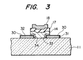
- Fig. 3 illustrates an example of a thin film transistor embodying the present invention, in which the parts corresponding to those in Fig. 1 are identified by the same reference numerals.
- drain and source electrodes 31 and 32 each of which is formed by a transparent conductive film on the transparent substrate 11, contain phosphorus, for instance.
- the phosphorus-doped transparent electrodes 31 and 32 can be formed by diffusing phosphorus into, for example, conventional transparent ITO films through an RF plasma assisted CVD process.
- the substrate 11 bearing an ITO film is heated to 200°C to 300°C, PH3 gas diluted with argon to 5000 ppm is passed over the ITO film of, for example, 50 to 200 nm (500 ⁇ to 2000 ⁇ ) thick, at a rate of 10 cc/min in an atmosphere held under a pressure of 13.33 KPa (102 Torr), and at the same time, a plasma assisted chemical vapor deposition is caused by an RF power of 20W for several minutes, thereby forming phosphorus-doped layers 30 in the ITO films.
- PH3 gas diluted with argon to 5000 ppm is passed over the ITO film of, for example, 50 to 200 nm (500 ⁇ to 2000 ⁇ ) thick, at a rate of 10 cc/min in an atmosphere held under a pressure of 13.33 KPa (102 Torr)
- a plasma assisted chemical vapor deposition is caused by an RF power of 20W for several minutes, thereby forming phosphorus-do
- the semiconductor layer 14 of amorphous silicon is formed, by the plasma assisted CVD method, on the phosphorus-doped transparent electrodes 31 and 32 thus obtained, indium and tin in the ITO films 31 and 32 are combined with phosphorus in the phosphorus-doped layers 30 and are difficult to migrate, and hence the indium and tin do not diffuse into the semiconductor layer 14.
- the phosphorus in the phosphorus-doped layers 30 in the transparent electrodes 31 and 32 partly migrates and diffuses into the semiconductor layer 14 over the entire areas of the contact surfaces of the transparent electrodes 31 and 32 with the semiconductor layer 14, forming ohmic contact layers 33 and 34 at the boundaries therebetween.
- the gate insulating film 17 and the gate electrode 18 are formed on the semiconductor layer 14 as in the prior art, thus obtaining a thin film transistor.
- the method for forming the phosphorus-doped ITO film is not limited specifically to the process utilizing the RF plasma assisted CVD technique, as referred to previously.
- the phosphorus can be thermally diffused into a phosphorus-free transparent conductive film by its heat treatment in an atmosphere containing, for example, the PH3 gas.
- the source of diffusion may be a liquid such as phosphorus oxychloride or a solid such as phosphorus pentoxide as well as the gas.
- the phosphorus-doped indium oxide or tin oxide conductive film by sputtering indium and/or tin in an atmosphere containing the PH3 gas, oxygen, and argon.
- phosphorus-doped ITO can also be obtained by spraying, for example, phosphrus chloride together with indium chloride and tin chloride.
- the ITO can also be formed through the plasma assisted CVD method using an atmosphere containing phosphorus oxychloride, oxygen and argon.
- the phosphorus-doped transparent conductive can be formed through ion implantation technique such that ionized phosphorus produced from an ion source of PH3 gas is accelerated by 30 to 100 KV and implanted into the transparent conductive film.
- the phosphorus-doped transparent conductive film thus obtained has substantially the same sheet resistance and light transmissivity as does a phosphorus-free transparent conductive film.
- the present invention it is possible to obtain a thin film transistor of excellent characteristics in which good ohmic contact is established between the source and drain transparent electrodes and a semiconductor layer, allowing excellent operation characteristics. Moreover, the use of the transparent conductive film of the present invention provides a solar cell of a high conversion efficiency. In either case, a good ohmic contact layer can be obtained without the necessity of involving any particular manufacturing step therefor.
Landscapes
- Electrodes Of Semiconductors (AREA)
- Photovoltaic Devices (AREA)
- Laminated Bodies (AREA)
- Manufacturing Of Electric Cables (AREA)
- Liquid Deposition Of Substances Of Which Semiconductor Devices Are Composed (AREA)
Abstract
Description
- The present invention relates to a transparent conductive film which is formed as a transparent electrode in contact with a semiconductor layer in a thin film transistor for use as a switching device of an active liquid crystal display device, or in a solar cell.
- For instance, an active liquid crystal display device employs a thin film transistor as a switching device. Conventionally, the thin film transistor has such a structure as depicted in Fig. 1. That is, drain and
source electrodes transparent substrate 11, and asemiconductor layer 14 of amorphous silicon or the like is formed between the drain andsource electrodes source electrodes ohmic contact layers 15 and 16 of n⁺ silicon so as to establish ohmic contact between theelectrodes amorphous semiconductor layer 14. Thesemiconductor layer 14 is covered with agate insulating film 17 of, for example, silicon nitride, which is, in turn, covered with agate electrode 18. - Another device which employs a transparent electrode provided in contact with a semiconductor layer is such a solar cell as shown in Fig. 2. In this case, a transparent
conductive film 22 is formed on atransparent substrate 21 as of glass, and p-type, i-type and n-typeconductive layers transparent electrode 22 in that order. Furthermore, anelectrode 26 of aluminum or similar material is deposited on top of the n-typeconductive layer 25. - In the manufacture of the device which has a transparent electrode formed in contact with a semiconductor layer, as described above, the amorphous
silicon semiconductor layer 14 in the thin film transistor or the p-type amorphous siliconconductive layer 23 in the solar cell is usually deposited through a plasma assisted CVD (Chemical Vapor Deposition) process. In this case, thesubstrate conductive films semiconductor layer 14 or p-typeconductive layer 23 adversely affecting the fabricated devices. - In the thin film transistor, the
ohmic contact layers 15 and 16 are each constituted by, for instance, an n⁺-type conductive layer, and if indium is diffused into the conductive layer, it will serve as a p-type impurity, making it impossible to obtain good ohmic contact. When indium is diffused into thesemiconductor layer 14, it acts as a p-type semiconductor, which impairs the operation characteristics of the thin transistor. Also in the solar cell, the diffusion of indium or tin from the transparentconductive film 22 into the p-type and i-typeconductive layers - It is therefore an object of the present invention to provide a transparent conductive film structure which permits excellent operations of a device of the type having a semiconductor layer and a transparent conductive film formed in contact with each other.
- According to one aspect of the present invention, there is provided a laminate of a transparent conductive film and a semiconductor layer, wherein said transparent conductive film is an ITO film containing phosphorus and is formed on an insulating substrate, said semiconductor layer being deposited on said ITO film to form an ohmic contact therewith and wherein at least the surface area of said semiconductor layer in contact with said ITO film contains phosphorus to form an ohmic contact layer.
- According to another aspect of the invention, there is provided a thin film transistor comprising source and drain electrodes formed of an ITO film containing phosphorus and deposited on an insulating substrate, and a semiconductor layer in ohmic contact with said source and drain electrodes and forming an active region of said thin film transistor, wherein the surface area of said semiconductor layer in contact with said ITO film contains phosphorus to form an ohmic contact layer.
- A further aspect of the invention provides a method of fabricating the above laminate or thin film transistor comprising the step of forming, on an insulating substrate, a transparent ITO film containing phosphorus, and the step of depositing the semiconductor layer on the ITO film
- The phosphorus forms an ohmic contact layer between the semiconductor layer and the transparent conductive film. Therefore, no particular step is needed for providing the ohmic contact layer.
- For a better understanding of the invention, and to show how the same may be carried into effect, reference will now be made, by way of example, to the accompanying drawings, in which:-
- Fig. 1 is a sectional view showing a conventional thin film transistor;
- Fig. 2 is a sectional view showing a conventional solar cell; and
- Fig. 3 is a sectional view illustrating a thin film transistor provided with the transparent conductive film according to the present invention.
- Fig. 3 illustrates an example of a thin film transistor embodying the present invention, in which the parts corresponding to those in Fig. 1 are identified by the same reference numerals. In this thin film transistor, drain and
source electrodes transparent substrate 11, contain phosphorus, for instance. The phosphorus-dopedtransparent electrodes substrate 11 bearing an ITO film is heated to 200°C to 300°C, PH₃ gas diluted with argon to 5000 ppm is passed over the ITO film of, for example, 50 to 200 nm (500 Å to 2000 Å) thick, at a rate of 10 cc/min in an atmosphere held under a pressure of 13.33 KPa (10² Torr), and at the same time, a plasma assisted chemical vapor deposition is caused by an RF power of 20W for several minutes, thereby forming phosphorus-dopedlayers 30 in the ITO films. - When the
semiconductor layer 14 of amorphous silicon is formed, by the plasma assisted CVD method, on the phosphorus-dopedtransparent electrodes ITO films layers 30 and are difficult to migrate, and hence the indium and tin do not diffuse into thesemiconductor layer 14. - Furthermore, the phosphorus in the phosphorus-doped
layers 30 in thetransparent electrodes semiconductor layer 14 over the entire areas of the contact surfaces of thetransparent electrodes semiconductor layer 14, formingohmic contact layers gate insulating film 17 and thegate electrode 18 are formed on thesemiconductor layer 14 as in the prior art, thus obtaining a thin film transistor. - The method for forming the phosphorus-doped ITO film, for instance, is not limited specifically to the process utilizing the RF plasma assisted CVD technique, as referred to previously. The phosphorus can be thermally diffused into a phosphorus-free transparent conductive film by its heat treatment in an atmosphere containing, for example, the PH₃ gas. In this instance, the source of diffusion may be a liquid such as phosphorus oxychloride or a solid such as phosphorus pentoxide as well as the gas. It is also possible to form the
transparent electrodes - It has been ascertained experimentally that the phosphorus-doped transparent conductive film thus obtained has substantially the same sheet resistance and light transmissivity as does a phosphorus-free transparent conductive film.
- As described above, according to the present invention, it is possible to obtain a thin film transistor of excellent characteristics in which good ohmic contact is established between the source and drain transparent electrodes and a semiconductor layer, allowing excellent operation characteristics. Moreover, the use of the transparent conductive film of the present invention provides a solar cell of a high conversion efficiency. In either case, a good ohmic contact layer can be obtained without the necessity of involving any particular manufacturing step therefor.
- It will be apparent that many modifications and variations may be effected without departing from the scope of the present invention as claimed.
Claims (19)
- A laminate of a transparent conductive film (31,32) and a semiconductor layer (14), wherein said transparent conductive film is an ITO film containing phosphorus and is formed on an insulating substrate (11), said semiconductor layer (14) being deposited on said ITO film to form an ohmic contact therewith, and wherein at least the surface area of said semiconductor layer (14) in contact with said ITO film (31,32) contains phosphorus to form an ohmic contact layer (33,34).
- A laminate of a transparent conductive film and a semiconductor layer according to claim 1, wherein the phosphorus is contained in the surface of said ITO film (31,32) in the form of a phosphorus-doped layer.
- A laminate of a transparent conductive film and a semiconductor layer according to claim 1, wherein said ITO film contains the phosphorus substantially all throughout its thickness.
- A thin film transistor comprising source and drain electrodes (31,32) formed of an ITO film containing phosphorus and deposited on an insulating substrate (11), and a semiconductor layer (14) in ohmic contact with said source and drain electrodes (31,32) and forming an active region of said thin film transistor, wherein the surface area of said semiconductor layer (14) in contact with said ITO film (31,32) contains phosphorus to form an ohmic contact layer (33,34).
- A method of fabricating a laminate according to claim 1 or a thin film transistor according to claim 4 comprising the step of forming, on an insulating substrate (11), a transparent ITO film (30,31,32) containing phosphorus and the step of depositing the semiconductor layer (14) on the ITO film.
- A fabricating method according to claim 5, wherein the transparent conductive film forming step comprises a first step of forming the transparent conductive film on the substrate and a second step of diffusing the phosphorus into the transparent conductive film.
- A fabricating method according to claim 6, wherein the second step consists of diffusing the phosphorus into the transparent conductive film through an RF plasma assisted chemical vapor deposition process.
- A fabricating method according to claim 7, wherein the second step consists in diffusing the phosphorus into the ITO film by passing PH₃ gas over it while heating the substrate.
- A fabricating method according to claim 6, wherein the second step consists in thermally diffusing phosphorus into the transparent conductive film.
- A fabricating method according to claim 9, wherein the transparent conductive film is heat treated for diffusing the phosphorus thereinto from a diffusion source containing phosphorus.
- A fabricating method according to claim 10, wherein the diffusion source is PH₃ gas.
- A fabricating method according to claim 10, wherein the diffusion source is phosphorus oxychloride.
- A fabricating method according to claim 10, wherein the diffusion source is phosphorus pentoxide.
- A fabricating method according to claim 5, wherein the transparent conductive film forming step consists in forming the transparent conductive film on the substrate through sputtering of phosphorus-containing indium tin oxide.
- A fabricating method according to claim 5, wherein the transparent conductive film forming step consists in forming the transparent conductive film on the substrate through vacuum evaporation of phosphorus-containing indium tin oxide.
- A fabricating method according to claim 5, wherein the transparent conductive film forming step consists in forming the transparent conductive film on the substrate through simultaneous sputtering of indium and tin in an atmosphere containing PH₃ gas and oxygen and argon.
- A fabricating method according to claim 5, wherein the transparent conductive film forming step consists in spraying onto the substrate phosphorus chloride along with indium chloride and tin chloride.
- A fabricating method according to claim 5, wherein the transparent conductive film forming step consists in forming said ITO film on the substrate by a plasma chemical vapor deposition process employing phosphorus oxychloride.
- A fabricating method according to claim 5, wherein the second step consists of introducing the phosphorus into the transparent conductive film by an ion implantation process.
Priority Applications (1)
| Application Number | Priority Date | Filing Date | Title |
|---|---|---|---|
| AT86113673T ATE72909T1 (en) | 1985-10-04 | 1986-10-03 | CLEAR CONDUCTIVE COATING AND METHOD FOR PRODUCTION. |
Applications Claiming Priority (2)
| Application Number | Priority Date | Filing Date | Title |
|---|---|---|---|
| JP60221665A JPS6281057A (en) | 1985-10-04 | 1985-10-04 | transparent conductive film |
| JP221665/85 | 1985-10-04 |
Publications (2)
| Publication Number | Publication Date |
|---|---|
| EP0217405A1 EP0217405A1 (en) | 1987-04-08 |
| EP0217405B1 true EP0217405B1 (en) | 1992-02-26 |
Family
ID=16770341
Family Applications (1)
| Application Number | Title | Priority Date | Filing Date |
|---|---|---|---|
| EP86113673A Expired - Lifetime EP0217405B1 (en) | 1985-10-04 | 1986-10-03 | Transparent conductive film and method of fabricating the same |
Country Status (6)
| Country | Link |
|---|---|
| US (1) | US4733284A (en) |
| EP (1) | EP0217405B1 (en) |
| JP (1) | JPS6281057A (en) |
| KR (1) | KR900007756B1 (en) |
| AT (1) | ATE72909T1 (en) |
| DE (1) | DE3683979D1 (en) |
Families Citing this family (19)
| Publication number | Priority date | Publication date | Assignee | Title |
|---|---|---|---|---|
| ATE77177T1 (en) * | 1985-10-04 | 1992-06-15 | Hosiden Corp | THIN FILM TRANSISTOR AND METHOD FOR ITS MANUFACTURE. |
| US4994401A (en) * | 1987-01-16 | 1991-02-19 | Hosiden Electronics Co., Ltd. | Method of making a thin film transistor |
| US5173443A (en) * | 1987-02-13 | 1992-12-22 | Northrop Corporation | Method of manufacture of optically transparent electrically conductive semiconductor windows |
| GB2214710A (en) * | 1988-01-29 | 1989-09-06 | Univ Open | Solar collectors |
| KR910007142A (en) * | 1988-09-30 | 1991-04-30 | 미다 가쓰시게 | Thin film phototransistor and optical sensor array using it |
| FR2640809B1 (en) * | 1988-12-19 | 1993-10-22 | Chouan Yannick | PROCESS FOR ETCHING A METAL OXIDE LAYER AND SIMULTANEOUSLY DEPOSITING A POLYMER FILM, APPLICATION OF THIS PROCESS TO THE MANUFACTURE OF A TRANSISTOR |
| JPH0391932A (en) * | 1989-09-04 | 1991-04-17 | Canon Inc | Manufacture of semiconductor device |
| KR930001901B1 (en) * | 1990-07-27 | 1993-03-19 | 삼성전자 주식회사 | Manufacturing Method of Thin Film Transistor |
| JP2912506B2 (en) * | 1992-10-21 | 1999-06-28 | シャープ株式会社 | Method for forming transparent conductive film |
| EP0660381A1 (en) * | 1993-12-21 | 1995-06-28 | Koninklijke Philips Electronics N.V. | Method of manufacturing a transparent conductor pattern and a liquid crystal display device |
| JP3272532B2 (en) * | 1993-12-27 | 2002-04-08 | 富士通株式会社 | Method for manufacturing semiconductor device |
| DE69635107D1 (en) * | 1995-08-03 | 2005-09-29 | Koninkl Philips Electronics Nv | SEMICONDUCTOR ARRANGEMENT WITH A TRANSPARENT CIRCUIT ELEMENT |
| US5824418A (en) * | 1995-09-05 | 1998-10-20 | Northrop Grumman Corporation | Optically transparent, electrically conductive semiconductor windows |
| JP2757850B2 (en) * | 1996-04-18 | 1998-05-25 | 日本電気株式会社 | Thin film transistor and method of manufacturing the same |
| KR100377376B1 (en) * | 2000-03-10 | 2003-03-26 | 우형철 | Ion Beam Assisted Evaporator and evaporating process thereof |
| US20070193624A1 (en) * | 2006-02-23 | 2007-08-23 | Guardian Industries Corp. | Indium zinc oxide based front contact for photovoltaic device and method of making same |
| JP4752712B2 (en) * | 2006-10-10 | 2011-08-17 | 株式会社島津製作所 | Automatic analyzer |
| US8179587B2 (en) * | 2008-01-04 | 2012-05-15 | 3M Innovative Properties Company | Electrochromic device |
| US8896065B2 (en) * | 2008-04-14 | 2014-11-25 | Sharp Laboratories Of America, Inc. | Top gate thin film transistor with independent field control for off-current suppression |
Family Cites Families (6)
| Publication number | Priority date | Publication date | Assignee | Title |
|---|---|---|---|---|
| FR1409894A (en) * | 1964-07-23 | 1965-09-03 | Electronique & Automatisme Sa | Advanced opto-electronic device |
| US4040073A (en) * | 1975-08-29 | 1977-08-02 | Westinghouse Electric Corporation | Thin film transistor and display panel using the transistor |
| US4278831A (en) * | 1979-04-27 | 1981-07-14 | The Boeing Company | Process for fabricating solar cells and the product produced thereby |
| JPS5951757B2 (en) * | 1979-12-27 | 1984-12-15 | 富士電機株式会社 | Method for manufacturing an amorphous semiconductor device |
| JPS5778135A (en) * | 1980-11-01 | 1982-05-15 | Semiconductor Energy Lab Co Ltd | Semiconductor device and manufacture thereof |
| JPS59181064A (en) * | 1983-03-31 | 1984-10-15 | Toshiba Corp | Semiconductor device |
-
1985
- 1985-10-04 JP JP60221665A patent/JPS6281057A/en active Pending
-
1986
- 1986-09-26 US US06/911,695 patent/US4733284A/en not_active Expired - Lifetime
- 1986-09-30 KR KR1019860008178A patent/KR900007756B1/en not_active Expired
- 1986-10-03 EP EP86113673A patent/EP0217405B1/en not_active Expired - Lifetime
- 1986-10-03 AT AT86113673T patent/ATE72909T1/en not_active IP Right Cessation
- 1986-10-03 DE DE8686113673T patent/DE3683979D1/en not_active Expired - Lifetime
Also Published As
| Publication number | Publication date |
|---|---|
| KR900007756B1 (en) | 1990-10-19 |
| EP0217405A1 (en) | 1987-04-08 |
| JPS6281057A (en) | 1987-04-14 |
| KR870004533A (en) | 1987-05-11 |
| ATE72909T1 (en) | 1992-03-15 |
| US4733284A (en) | 1988-03-22 |
| DE3683979D1 (en) | 1992-04-02 |
Similar Documents
| Publication | Publication Date | Title |
|---|---|---|
| US4733284A (en) | Semiconductor devices and laminates including phosphorus doped transparent conductive film | |
| US4864376A (en) | Thin-film transistor and method of fabricating the same | |
| US4849797A (en) | Thin film transistor | |
| US5589694A (en) | Semiconductor device having a thin film transistor and thin film diode | |
| US4624045A (en) | Method of making thin film device | |
| KR100299555B1 (en) | Thin-film transistors with high resistance back channel area and manufacturing method | |
| EP0060363B1 (en) | Method of manufacture of a pin amorphous silicon semi-conductor device | |
| US4261095A (en) | Self aligned schottky guard ring | |
| JPS58115864A (en) | Semiconductor device | |
| US4387387A (en) | PN Or PIN junction type semiconductor photoelectric conversion device | |
| US6087205A (en) | Method of fabricating staggered thin film transistor with an improved ohmic contact structure | |
| US4446168A (en) | Method of forming amorphous silicon | |
| US4349395A (en) | Method for producing MOS semiconductor device | |
| GB2077996A (en) | Method of manufacturing solar cells | |
| US3460240A (en) | Manufacture of semiconductor solar cells | |
| JPH01309378A (en) | Thin-film semiconductor element | |
| JPS61159771A (en) | photovoltaic device | |
| JPH0564862B2 (en) | ||
| US4734379A (en) | Method of manufacture of solar battery | |
| JP3079566B2 (en) | Thin film transistor and method of manufacturing the same | |
| KR19990046858A (en) | Thin film transistor for liquid crystal display device and manufacturing method | |
| JPH0228906B2 (en) | ||
| JPH02196470A (en) | Thin film transistor and manufacture thereof | |
| JPH0330296B2 (en) | ||
| JPH02210882A (en) | Phototransistor and its manufacturing method |
Legal Events
| Date | Code | Title | Description |
|---|---|---|---|
| PUAI | Public reference made under article 153(3) epc to a published international application that has entered the european phase |
Free format text: ORIGINAL CODE: 0009012 |
|
| 17P | Request for examination filed |
Effective date: 19861003 |
|
| AK | Designated contracting states |
Kind code of ref document: A1 Designated state(s): AT BE CH DE ES FR GB GR IT LI LU NL SE |
|
| 17Q | First examination report despatched |
Effective date: 19900117 |
|
| GRAA | (expected) grant |
Free format text: ORIGINAL CODE: 0009210 |
|
| AK | Designated contracting states |
Kind code of ref document: B1 Designated state(s): AT BE CH DE ES FR GB GR IT LI LU NL SE |
|
| PG25 | Lapsed in a contracting state [announced via postgrant information from national office to epo] |
Ref country code: IT Free format text: LAPSE BECAUSE OF FAILURE TO SUBMIT A TRANSLATION OF THE DESCRIPTION OR TO PAY THE FEE WITHIN THE PRESCRIBED TIME-LIMIT;WARNING: LAPSES OF ITALIAN PATENTS WITH EFFECTIVE DATE BEFORE 2007 MAY HAVE OCCURRED AT ANY TIME BEFORE 2007. THE CORRECT EFFECTIVE DATE MAY BE DIFFERENT FROM THE ONE RECORDED. Effective date: 19920226 Ref country code: SE Effective date: 19920226 Ref country code: LI Effective date: 19920226 Ref country code: GR Free format text: LAPSE BECAUSE OF FAILURE TO SUBMIT A TRANSLATION OF THE DESCRIPTION OR TO PAY THE FEE WITHIN THE PRESCRIBED TIME-LIMIT Effective date: 19920226 Ref country code: CH Effective date: 19920226 Ref country code: AT Effective date: 19920226 Ref country code: BE Effective date: 19920226 |
|
| REF | Corresponds to: |
Ref document number: 72909 Country of ref document: AT Date of ref document: 19920315 Kind code of ref document: T |
|
| RAP2 | Party data changed (patent owner data changed or rights of a patent transferred) |
Owner name: HOSIDEN CORPORATION |
|
| REF | Corresponds to: |
Ref document number: 3683979 Country of ref document: DE Date of ref document: 19920402 |
|
| PG25 | Lapsed in a contracting state [announced via postgrant information from national office to epo] |
Ref country code: ES Free format text: LAPSE BECAUSE OF FAILURE TO SUBMIT A TRANSLATION OF THE DESCRIPTION OR TO PAY THE FEE WITHIN THE PRESCRIBED TIME-LIMIT Effective date: 19920606 |
|
| ET | Fr: translation filed | ||
| REG | Reference to a national code |
Ref country code: CH Ref legal event code: PL |
|
| PG25 | Lapsed in a contracting state [announced via postgrant information from national office to epo] |
Ref country code: LU Free format text: LAPSE BECAUSE OF NON-PAYMENT OF DUE FEES Effective date: 19921031 |
|
| PLBE | No opposition filed within time limit |
Free format text: ORIGINAL CODE: 0009261 |
|
| STAA | Information on the status of an ep patent application or granted ep patent |
Free format text: STATUS: NO OPPOSITION FILED WITHIN TIME LIMIT |
|
| BECN | Be: change of holder's name |
Effective date: 19920226 |
|
| 26N | No opposition filed | ||
| NLT1 | Nl: modifications of names registered in virtue of documents presented to the patent office pursuant to art. 16 a, paragraph 1 |
Owner name: HOSIDEN CORPORATION TE YAO, JAPAN. |
|
| PGFP | Annual fee paid to national office [announced via postgrant information from national office to epo] |
Ref country code: FR Payment date: 19970922 Year of fee payment: 12 |
|
| PGFP | Annual fee paid to national office [announced via postgrant information from national office to epo] |
Ref country code: GB Payment date: 19970924 Year of fee payment: 12 |
|
| PGFP | Annual fee paid to national office [announced via postgrant information from national office to epo] |
Ref country code: NL Payment date: 19971031 Year of fee payment: 12 |
|
| PGFP | Annual fee paid to national office [announced via postgrant information from national office to epo] |
Ref country code: DE Payment date: 19971114 Year of fee payment: 12 |
|
| REG | Reference to a national code |
Ref country code: FR Ref legal event code: TP |
|
| NLS | Nl: assignments of ep-patents |
Owner name: HOSIDEN AND PHILIPS DISPLAY CORPORATION |
|
| REG | Reference to a national code |
Ref country code: GB Ref legal event code: 732E |
|
| PG25 | Lapsed in a contracting state [announced via postgrant information from national office to epo] |
Ref country code: GB Free format text: LAPSE BECAUSE OF NON-PAYMENT OF DUE FEES Effective date: 19981003 |
|
| PG25 | Lapsed in a contracting state [announced via postgrant information from national office to epo] |
Ref country code: NL Free format text: LAPSE BECAUSE OF NON-PAYMENT OF DUE FEES Effective date: 19990501 |
|
| GBPC | Gb: european patent ceased through non-payment of renewal fee |
Effective date: 19981003 |
|
| PG25 | Lapsed in a contracting state [announced via postgrant information from national office to epo] |
Ref country code: FR Free format text: LAPSE BECAUSE OF NON-PAYMENT OF DUE FEES Effective date: 19990630 |
|
| NLV4 | Nl: lapsed or anulled due to non-payment of the annual fee |
Effective date: 19990501 |
|
| REG | Reference to a national code |
Ref country code: FR Ref legal event code: ST |
|
| PG25 | Lapsed in a contracting state [announced via postgrant information from national office to epo] |
Ref country code: DE Free format text: LAPSE BECAUSE OF NON-PAYMENT OF DUE FEES Effective date: 19990803 |