EP0213562B2 - Signalverarbeitungsanordnung mit einem Feldeffekttransistor und bipolaren Transistoren - Google Patents
Signalverarbeitungsanordnung mit einem Feldeffekttransistor und bipolaren Transistoren Download PDFInfo
- Publication number
- EP0213562B2 EP0213562B2 EP86111595A EP86111595A EP0213562B2 EP 0213562 B2 EP0213562 B2 EP 0213562B2 EP 86111595 A EP86111595 A EP 86111595A EP 86111595 A EP86111595 A EP 86111595A EP 0213562 B2 EP0213562 B2 EP 0213562B2
- Authority
- EP
- European Patent Office
- Prior art keywords
- signal
- bipolar transistor
- base
- npn bipolar
- transistor
- Prior art date
- Legal status (The legal status is an assumption and is not a legal conclusion. Google has not performed a legal analysis and makes no representation as to the accuracy of the status listed.)
- Expired - Lifetime
Links
Images


Classifications
-
- H—ELECTRICITY
- H03—ELECTRONIC CIRCUITRY
- H03D—DEMODULATION OR TRANSFERENCE OF MODULATION FROM ONE CARRIER TO ANOTHER
- H03D7/00—Transference of modulation from one carrier to another, e.g. frequency-changing
- H03D7/12—Transference of modulation from one carrier to another, e.g. frequency-changing by means of semiconductor devices having more than two electrodes
-
- H—ELECTRICITY
- H03—ELECTRONIC CIRCUITRY
- H03G—CONTROL OF AMPLIFICATION
- H03G1/00—Details of arrangements for controlling amplification
- H03G1/0005—Circuits characterised by the type of controlling devices operated by a controlling current or voltage signal
- H03G1/0035—Circuits characterised by the type of controlling devices operated by a controlling current or voltage signal using continuously variable impedance elements
- H03G1/0082—Circuits characterised by the type of controlling devices operated by a controlling current or voltage signal using continuously variable impedance elements using bipolar transistor-type devices
Definitions
- the present invention relates to a signal-processing circuit having a field-effect transistor and a bipolar transistor connected in cascade to the field-effect transistor.
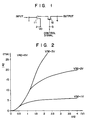
- a gain-controlled amplifier for use in a high-frequency amplifying stage, such as a tuner, has the structure shown in Fig. 1 or that shown in Fig. 4.
- the amplifier of Fig. 1 is disclosed in Japanese Patent Disclosure Sho 61-160170.
- This circuit comprises a MOSFET 11 (metal oxide semiconductor field-effect transistor) used as the first stage, and another MOSFET 12 used as the second stage and cascade-connected to MOSFET 11.
- the gate of FET 11 is connected to input terminal 1 which in turn is coupled to an input tuning circuit (not shown), and can receive a DC bias signal and an input signal from the tuning circuit via input terminal 1.
- a predetermined voltage (usually, the ground potential) is applied to the gate of FET 12 through gain control terminal 3.
- the drain of FET 12 is connected to output terminal 4.
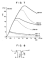
- the amplifier shown in Fig. 4 is disclosed in Integrated Electronics, McGraw-Hill, Inc., pp 566-569.
- This circuit comprises an NPN transistor 13 used as the first stage, and an NPN transistor 14 used as the second state and which is cascade-connected to NPN transistor 13.
- the base of transistor 13 is coupled to input terminal 1.
- the emitter of transistor 14 is connected to terminal 2 held at a predetermined potential.
- the base and collector of transistor 14 are connected to gain control terminal 3 and output terminal 4, respectively.
- the amplifier of Fig. 1 amplifies the signal supplied to input terminal 1 when a predetermined operation current flows through first-stage FET 11 and second-stage FET 12.
- the amplifier has one drawback, however. Its input-output characteristic contains prominent third order distortion components. This is because the MOSFETs have a high equivalent resistance, due to their structure and function. More specifically, the amplifier exhibits the DC input-output characteristics shown in Fig. 2, when a gain control voltage is applied to the gate of FET 12.
- the DC input-output characteristic is the relation between voltage V12 between terminals 1 and 2, and current I42 flowing between terminals 2 and 4.
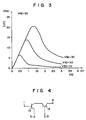
- FIG. 3 correspond to the third order distortion components of the input-output characteristic curve (Fig. 2).
- Fig. 3 clearly shows, there are inflection points where the slope of the characteristic curve is steep. This means that the characteristic curve has prominent third order distortion components.
- Fig. 3 further reveals that there are two inflection points where gain-controlling voltage V32 falls. If such is the case, the third order distortion components will become more prominent.
- the equivalent resistance of the collector-emitter path of transistor 13 is far lower than that of either MOSFET used in the amplifier of Fig. 1.
- the input-output characteristic curve of the amplifier shown in Fig. 4 also has prominent third order distortion components. This is inevitably because the first-stage transistor is a bipolar transistor.
- Prior art document DE-A-15 12 683 discloses an amplifying circuit in which a source-drain-path of a FET is connected in series with an emitter-collector-path of a bipolar transistor between earth potential and an output terminal, wherein an input signal is supplied to the gate terminal of the FET, and a control voltage is applied to the base terminal of the bipolar transistor.
- a voltage divider consisting of three resistors is provided between the gate terminal of the bipolar transistor and the gate terminal of the FET.
- a skilled person working on a circuit as disclosed by above document DE-A-15 12 683 can, for example, easily have the problem that the source delivering a second signal has a very limited capacity in delivering current to drive the bipolar transistor, i.e. that the bipolar transistor does not have an adequate current amplification.
- document DE-A-1 806 338 includes blocking off of high frequencies via a capacitor arrangement.
- document GB-A-2 002 608 mentions filtering high frequency components from the control signal.
- the present invention provides a signal-processing circuit as specified in claim 1 or 3.
- the first signal can therefore be controlled by the second signal.
- the signal-processing circuit can have an input-output characteristic curve with negligible distortion components, particularly negligible third order distortion components.
- Fig. 5 is a circuit diagram of a gain-controlled amplifier.
- the source of N-channel enhancement or depletion enhancement MOSFET 21 is connected to terminal 2 to which a predetermined potential (usually, the ground potential) is applied.
- the gate of FET 21 is coupled to input terminal 1 which in turn is connected to input tuning circuit 23.
- the emitter of NPN bipolar transistor 22 is connected to the drain of FET 21.
- the base of NPN transistor 22 is coupled to gain control terminal 3 which in turn is connected to gain control circuit 24.
- the collector of NPN transistor 22 is connected to output terminal 4 coupled to output tuning circuit 25.
- Input tuning circuit 23 receives a high-frequency signal obtained from, for example, VHF-band TV waves. Circuit 23 supplies this high-frequency signal and, if necessary, a DC bias signal to input terminal 1. As a result, a predetermined operation current flows from the power source of output tuning circuit25 to terminal 2 through terminal 4, the collector-emitter path of NPN transistor 22 and the current path of FET 21. As this current flows through both transistors 21 and 22, the input signal, i.e., the high-frequency signal, is amplified with the gain corresponding to the gain-controlling voltage applied to the base of transistor 22.
- Input voltage V12 i.e., the voltage between terminals 1 and 2
- output current I42 i.e., the current between terminals 4 and 2
- operation voltage V42 i.e., the voltage between terminals 4 and 2
- control voltage V32 i.e., the voltage between terminals 3 and 2
- the first order distortion components and second order distortion components of the characteristic curve are also less prominent than those of the characteristic curve of the conventional amplifier (Fig. 1).
- the gain changes in accordance with control voltage V12, same as the conventional gain-controlled amplifiers shown in Figs. 1 and 4.
- the gain-controlled amplifier of this embodiment can therefore generate an output signal containing distortion components which are less prominent than those of the output signal produced by the conventional gain-controlled amplifiers.
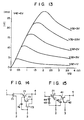
- Fig. 8 The modification of Fig. 8 is characterized in two respects. First, resistor 31 for adjusting the base current of second-stage transistor 22 and protecting the base of transistor 22, is connected between the base of transistor 22 and gain control terminal 3. Secondly, capacitor 32 for grounding high-frequency components of a signal, is connected between the base of transistor 22 and gain control terminal 3. Forward transmission admittance
- Fig. 9 The modification shown in Fig. 9 is also characterized in two respects. First, Darlington-connected NPN transistors 41 and 42 are used in place of second-stage transistor 22. Secondly, capacitor 43 for grounding the high-frequency components of a signal, is connected between the base of transistor 41 and gain control terminal 3. Capacitor 43 can be coupled between the source of FET 21 and the base of transistor 41.
- Fig. 10 which is an embodiment of the invention has three characterizing features.
- Darlington-connected NPN transistors 51 and 52 are used in place of second-stage transistor 22.
- resistor 53 for adjusting the base current of transistor 52 is coupled between the base of transistor 52 and gain control terminal 3.
- capacitor 54 for grounding the high-frequency components of a signal is connected between the base of transistor 51 and gain control terminal 3.
- FET 61 The capacitance between the drain and source of FET 61 should ideally be small. Otherwise, an excessive capacitance will be added between the collector and emitter of transistor 22. For this reason, FET 61 should have similar high-frequency characteristic and are highly sensitive (that is, having a high mutual conductance), same as FET 21.
- the gate voltage of FET 61 is controlled, thereby controlling the drain current of FET 61.
- the base current of transistor 22 is controlled.
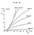
- the amplifier has the input-output characteristic shown in Fig. 12. Its forward transmission admittance
- Fig. 14 shows a modification of the second embodiment (Fig. 11). This modification differs from the amplifier of Fig. 11 in three respects. First, Darlington-connected NPN transistors 71 and 72 are used in place of second-stage bipolar transistor 22. Secondly, the current path of control FET 73 is connected between the collector and base of transistor 72. Thirdly, capacitor 74 for grounding the high-frequency components of a signal, is coupled between the base of transistor 71 and gain control terminal 3. If control FET 73 has excellent DC characteristics, the modification of Fig. 14 can have as good an input-output characteristic as the amplifier of Fig. 5 and second embodiments shown in Fig. 11.
- a high-frequency input signal is supplied to terminal 1 (in other words, the gate of transistor 21), and a gain control voltage is applied to terminal 3, thereby amplifying the high-frequency input signal by the gain corresponding to the gain control voltage.
- the present invention is not limited to these embodiments.
- Other input signals such as a low-frequency signal or an intermediate-frequency signal, can be amplified.
- first and second signals can be input to terminals 1 and 3, whereby they are mixed.
- circuits of the above embodiments can be manufactured either in the form of an integrated circuit made by a bipolar/MOS process, or in the form of an assembly of independently made elements.
- the circuits can be manufactured using compound semiconductor, for example GaAs.
- the amplifier shown in Fig. 15 which is a modification of the amplifier shown in Fig. 9, be formed on one pellet mode of silicon, by a bipolar/MOS process, in the form of an integrated circuit is described.
- the amplifier of Fig. 15 is different from that of Fig. 9 in two respects.
- capacitor 43 is connected at one end to the source of FET 21.
- a bidirectional diode consisting of protective diodes 44 and 45 connected in series and arranged in opposite directions, is connected between the gate and source of FET 21, thus protecting the gate of FET 21.
- Fig. 16 is a cross-sectional view of the amplifier of Fig. 15, formed in or on a p-type silicon substrate.
- Fig. 17 is a cross-sectional view of the same amplifier formed on an n-type silicon substrate.
- p-type epitaxial layer 110B is formed on p-type silicon substrate 110A.
- Buried layer 113 having a high n-type impurity concentration (n + -type) is formed at the interface between silicon substrate 110A and epitaxial layer 110B.
- Region 115 is shaped like a ring and surrounds well region 114, for example.
- p-type regions 116 and 117 are formed, set apart from each other.
- n-type region 118 is formed in the surface region of p-type region 116, and another n-type region 119 is formed in the surface region of p-type region 117.
- Oxide film 120A is formed on epitaxial layer 110B. Five contact holes are cut in those portions of oxide film 120A which are provided on n + -type region 115, p-type regions 116 and 117, and n-type regions 118 and 119.
- Electrodes 121, 122, 123, and 124 made of aluminum are formed on oxide film 120A. Electrode 121 contacts n + -type region 115. Electrode 122 contacts p-type region 117. Electrode 123 connects p-type region 16 and n-type region 119. Electrode 124 connects n-type region 118 to n-type region 125 corresponding to drain D of MOSFET 21.
- n-type well region 114, p-type region 116, and n-type region 118 correspond to the collector, base, and emitter of first-stage transistor 21 (Fig. 15), respectively
- n-type well region 114, p-type region 117, and n-type region 119 correspond to the collector, base, and emitter of second-stage transistor 42 (Fig. 15), respectively.
- Electrodes 121 and 122 correspond, respectively, to output terminal 4 and gain control terminal 3, both shown in Fig. 15.
- n-type regions 125, 126, and 127, and p + -type region 128 are formed in a surface region of epitaxial layer 110B.
- p + -type region 129 is formed in the surface region of n-type region 127.
- Another p + -type region 130 is formed partly in n-type region 127 and partly in the surface region of epitaxial layer 110B.
- Insulation film 120B i.e., gate oxide film
- Gate electrode 131 is formed on insulation film 120B.
- Thin oxide film 120C is formed on one portion of p + -type region 128.
- Aluminum electrode 132 is formed on thin oxide film 120C.
- Six contact holes are cut in those portions of oxide film 120A formed on epitaxial layer 110B, which are located in n-type regions 125 and 126, p + -type regions 128, 129, and 130, and gate electrode 131.
- Electrodes 133, 134, 135, 136, and 137 made of aluminum, are formed on oxide film 120A.
- Electrode 133 contacts n-type region 126.
- Electrodes 134, 135, and 136 contact p + -type regions 128, 129, and 130, respectively.
- Electrode 137 contacts gate electrode 131.
- N-type regions 125 and 126, and gate electrode 131 correspond to the drain, source, and gate of FET 21 (Fig. 15), respectively.
- Electrodes 137 and 133 correspond to input terminal 1 and terminal 2 (both shown in Fig. 15), respectively.
- Electrodes 132 and 134 correspond to the electrodes of capacitor 43 (Fig. 15). Electrodes 132 and 134 are connected by aluminum wires (not shown) to electrodes 123 and 133, respectively.
- Electrodes 135 and 136 correspond, respectively, to the anodes of diodes 44 and 45, and are connected to electrodes 137 and 133 by wired (not shown).
- the circuit shown in Fig. 15 is made in the form of a pellet, and is attached to a lead frame (not shown) by gold-silicon eutectic or by a resin.
- the lead terminals corresponding to terminals 1, 3, and 4, and electrodes 137, 122, and 121 corresponding to input terminal 1, gain control terminal 3, and output terminal 4, are connected by a wire-bonding.
- an oxide film is formed on one major surface of p-type silicon substrate 110A doped with boron in a concentration of, for example, 4 x 10 14 cm -3
- the oxide film is patterned, exposing that portion of substrate 110A in which buried layer 113 will be formed.
- Antimony in a concentration of 5 x 10 19 cm -3 is diffused into substrate 110A, using the patterned oxide film as the diffusion mask, thereby forming n + -type buried layer 113.
- Epitaxial layer 110B of silicon containing boron in a concentration 1.8 x 10 15 cm -3 is formed on substrate 110A; this epitaxial layer has a thickness of 7 to 8 ⁇ m.
- An oxide film is then formed on epitaxial layer 110B.
- This oxide film is patterned, exposing those portions of epitaxial layer 110B in which regions 114, 115, and 127 will be formed.
- phosphorus is ion-implanted into epitaxial layer 110B, under acceleration voltage of 150 kev, in a dosage of 1 x 10 15 cm -2 , thereby forming regions 114 and 127, and under acceleration voltage of 50 kev, in a dosage of 9 x 10 15 cm -2 , thereby forming region 115.
- PSG is deposited in the openings of the oxide film.
- the resultant structure is annealed for 15 hours at 1200°C in a nitrogen gas atmosphere.
- n-type well region 114, n + -type region 115, and n-type region 127 are completed.
- Another oxide film is formed on the surface of the unfinished product, and has a thickness of 180 nm. This oxide film is patterned, to form regions 116, 117, 128, 129, and 130. Using the patterned oxide film as mask, boron is ion-implanted into epitaxial layer 110B under acceleration voltage of 50 kev, in a dosage of 1 x 10 14 cm -2 , and the resultant structure is annealed for 30 minutes at 1000°C in a nitrogen atmosphere, thus forming p-type regions 116 and 117.
- boron is ion-implanted into epitaxial layer 110B under acceleration voltage of 50 kev, in a dosage of 1 x 10 14 cm -2 , and the unfinished product is annealed for 30 minutes at 1000°C in a nitrogen gas atmosphere, thereby forming p + -type regions 128, 129, and 130.
- gate oxide film 120B and oxide film 120C for forming a capacitor are formed.
- Gate electrode 131 having a width of 1.5 ⁇ m is formed of molybdenum silicide (MoSi).
- MoSi molybdenum silicide
- gate electrode 131 arsenic is ion-implanted into regions 116 and 117 under acceleration voltage of 35 kev, in a dosage of 1 x 10 15 cm -2 , and the resultant structure is annealed for 20 minutes at 1000°C in a nitrogen gas atmosphere, thereby forming n-type regions 118 and 119.
- the oxide film is patterned, thus making contact holes.
- the unfinished product is subjected to thermal oxidation, whereby oxide film 120A is formed.
- An aluminum film is then formed on oxide film 120A.
- the aluminum film is patterned, thereby forming electrodes 121-124 and electrodes 132-137.
- the gain-controlled amplifier shown in Fig. 17 differs from the gain-controlled amplifier of Fig. 16 in the following respects:
- Fig. 17 is the same as that of Fig. 16. Therefore, the same elements as those used in the amplifier shown in Fig. 16 are designated by the same numerals in Fig. 17, and are therefore not described.
- the signal-processing circuit of this invention can be used as a gain controlled amplifiers, since its input-output characteristic curve has far less third order distortion components as compared to the characteristic curves of the conventional gain-controlled amplifiers. Hence, it can operate effectively, particularly when it is used as a high-frequency amplifier whose gain is controlled by AGC (automatic gain control) feedback voltage. Further, when the signal-processing circuit is employed as a mixing circuit, it can generate an output signal having negligibly small distortion components; in particularly, negligible third order distortion components.
Landscapes
- Engineering & Computer Science (AREA)
- Power Engineering (AREA)
- Amplifiers (AREA)
Claims (4)
- Signalverarbeitungsschaltung mit:einer Einrichtung (1) zum Empfangen eines ersten Signals;einem MOSFET (Metalloxid-Halbleiter-Feldeffekttransistor) (21), dessen Gate an der Einrichtung (1) zum Empfang des ersten Signals angeschlossen ist und dessen Strompfad an einem Ende (2) mit einem vorgegebenen Potential beaufschlagt ist;einer Einrichtung (3) zum Empfangen eines zweiten Signals;einer Einrichtung (4) zum Absetzen eines Ausgangssignals; undeinem ersten npn -Bipolartransistor (51), dessen Kollektor-Emitter-Pfad an einem Ende mit dem anderen Ende des Strompfades des MOSFET (21) und am anderen Ende mit der Einrichtung (4) zum Absetzen des Ausgangssignals gekoppelt ist;gekennzeichnet durch:einen zweiten npn-Bipolartransistor (52), dessen Kollektor-Emitter-Pfad an einem Ende mit der Basis des ersten npn-Bipolartransistors (51) und am anderen Ende mit der Einrichtung (4) zum Absetzen des Ausgangssignals gekoppelt ist und der den Basisstrom des ersten npn-Bipolartransistors (51) gemäß dem zweiten Signal steuert;eine Widerstandseinrichtung (53) zur Strombegrenzung, die mit einem Anschluß an die Basis des zweiten npn-Bipolartransistors (52) und mit einem anderen Anschluß an die Einrichtung (3) zum Empfang des zweiten Signals gekoppelt ist; undeinen Kondensator (54) mit einem mit der Basis des ersten npn-Bipolartransistors (51) verbundenen Anschluß und einem anderen Anschluß, an den ein Potential angelegt ist, zum Legen der Basis des ersten npn-Bipolartransistors (51) an Masse, wenn der erste npn-Bipolartransistors (51) bei hohen Frequenzen aktiviert ist.
- Schaltung nach Anspruch 1, dadurch gekennzeichnet, daß der andere Anschluß des Kondensators (54) mit der Empfangseinrichtung (3) verbunden ist, um so das zweite Signal zu empfangen.
- Signalverarbeitungsschaltung mit:einer Einrichtung (1) zum Empfangen eines ersten Signals;einem ersten MOSFET (Metalloxid-Halbleiter-Feldeffekttran-sistor) (21), dessen Gate an der Einrichtung (1) zum Empfang des ersten Signals angeschlossen ist und dessen Strompfad an einem Ende (2) mit einem vorgegebenen Potential beaufschlagt ist;einer Einrichtung (3) zum Empfangen eines zweiten Signals;einer Einrichtung (4) zum Absetzen eines Ausgangssignals; undeinem npn-Bipolartransistor (22), dessen Kollektor-Emitter-Pfad an einem Ende mit dem anderen Ende des Strompfades des ersten MOSFET (21) und am anderen Ende mit der Einrichtung (4) zum Absetzen des Ausgangssignals gekoppelt ist;gekennzeichnet durch:einen zweiten MOSFET (61), dessen Strompfad an einem Ende mit der Basis des npn-Bipolartransistors (22) und am anderen Ende mit der Einrichtung (4) zum Absetzen des Ausgangssignals gekoppelt ist, dessen Gate mit der Einrichtung (3) zum Empfang des zweiten Signals gekoppelt ist und der den Basisstrom des npn-Bipolartransistors (22) gemäß dem zweiten Signal steuert; undeinen Kondensator (62) mit einem mit der Basis des npn-Bipolartransistors (22) verbundenen Anschluß und einem anderen Anschluß, an den ein Potential angelegt ist, zum Legen der Basis des npn-Bipolartransistors (22) an Masse, wenn der erste npn-Bipolartransistors (22) bei hohen Frequenzen aktiviert ist.
- Schaltung nach Anspruch 3, dadurch gekennzeichnet, daß der andere Anschluß des Kondensators (62) mit der Empfangseinrichtung (3) zum Empfang des zweiten Signals verbunden ist.
Applications Claiming Priority (4)
| Application Number | Priority Date | Filing Date | Title |
|---|---|---|---|
| JP18923285 | 1985-08-28 | ||
| JP189232/85 | 1985-08-28 | ||
| JP72950/86 | 1986-03-31 | ||
| JP61072950A JPS62122307A (ja) | 1985-08-28 | 1986-03-31 | 利得制御増幅回路 |
Publications (4)
| Publication Number | Publication Date |
|---|---|
| EP0213562A2 EP0213562A2 (de) | 1987-03-11 |
| EP0213562A3 EP0213562A3 (en) | 1989-03-15 |
| EP0213562B1 EP0213562B1 (de) | 1993-01-13 |
| EP0213562B2 true EP0213562B2 (de) | 1997-11-12 |
Family
ID=26414084
Family Applications (1)
| Application Number | Title | Priority Date | Filing Date |
|---|---|---|---|
| EP86111595A Expired - Lifetime EP0213562B2 (de) | 1985-08-28 | 1986-08-21 | Signalverarbeitungsanordnung mit einem Feldeffekttransistor und bipolaren Transistoren |
Country Status (3)
| Country | Link |
|---|---|
| US (1) | US4757276A (de) |
| EP (1) | EP0213562B2 (de) |
| DE (1) | DE3687494T3 (de) |
Families Citing this family (13)
| Publication number | Priority date | Publication date | Assignee | Title |
|---|---|---|---|---|
| US5212398A (en) * | 1989-11-30 | 1993-05-18 | Kabushiki Kaisha Toshiba | BiMOS structure having a protective diode |
| US5086282A (en) * | 1990-10-05 | 1992-02-04 | Allied-Signal Inc. | Field effect transistor-bipolar transistor Darlington pair |
| US5187110A (en) * | 1990-10-05 | 1993-02-16 | Allied-Signal Inc. | Field effect transistor-bipolar transistor darlington pair |
| JP3161721B2 (ja) * | 1990-10-19 | 2001-04-25 | 株式会社日立製作所 | 増幅回路及びディスプレイ装置 |
| US5748035A (en) * | 1994-05-27 | 1998-05-05 | Arithmos, Inc. | Channel coupled feedback circuits |
| US5920230A (en) * | 1997-10-21 | 1999-07-06 | Trw Inc. | HEMT-HBT cascode distributed amplifier |
| US6184751B1 (en) * | 1998-08-17 | 2001-02-06 | Motorola, Inc. | Amplifier circuit |
| JP2000209115A (ja) * | 1999-01-18 | 2000-07-28 | Alps Electric Co Ltd | チュ―ナ |
| JP2000278109A (ja) * | 1999-03-19 | 2000-10-06 | Fujitsu Ltd | 高周波スイッチ、切替型高周波スイッチ、および切替型高周波電力増幅器 |
| RU2292997C2 (ru) * | 2003-10-08 | 2007-02-10 | Хитачи Коки Ко. Лтд. | Станок для резки под углом с индикацией угла установки режущего элемента (варианты) |
| JP2006135518A (ja) * | 2004-11-04 | 2006-05-25 | Alps Electric Co Ltd | 高周波増幅器 |
| DE102013206412A1 (de) * | 2013-04-11 | 2014-10-16 | Ifm Electronic Gmbh | Schutzschaltung für eine Signalausgangs-Stufe |
| CN103644303A (zh) * | 2013-11-17 | 2014-03-19 | 苏州蓝王机床工具科技有限公司 | 皮带运输机托辊轴端密封圈结构 |
Family Cites Families (6)
| Publication number | Priority date | Publication date | Assignee | Title |
|---|---|---|---|---|
| GB1178232A (en) * | 1966-02-12 | 1970-01-21 | Emi Ltd | Improvements in or relating to gain control circuits. |
| US3541234A (en) * | 1967-10-20 | 1970-11-17 | Rca Corp | Video circuits employing cascoded combinations of field effect transistors with high voltage,low bandwidth bipolar transistors |
| US3609479A (en) * | 1968-02-29 | 1971-09-28 | Westinghouse Electric Corp | Semiconductor integrated circuit having mis and bipolar transistor elements |
| JPS5315638B2 (de) * | 1972-12-13 | 1978-05-26 | ||
| GB2002608B (en) * | 1977-08-01 | 1982-03-24 | Pioneer Electronic Corp | Automatic gain control circuit |
| US4586004A (en) * | 1983-06-27 | 1986-04-29 | Saber Technology Corp. | Logic and amplifier cells |
-
1986
- 1986-08-21 EP EP86111595A patent/EP0213562B2/de not_active Expired - Lifetime
- 1986-08-21 DE DE3687494T patent/DE3687494T3/de not_active Expired - Lifetime
- 1986-08-25 US US06/899,592 patent/US4757276A/en not_active Expired - Lifetime
Also Published As
| Publication number | Publication date |
|---|---|
| DE3687494D1 (de) | 1993-02-25 |
| EP0213562A2 (de) | 1987-03-11 |
| US4757276A (en) | 1988-07-12 |
| DE3687494T2 (de) | 1993-04-29 |
| DE3687494T3 (de) | 1998-06-10 |
| EP0213562A3 (en) | 1989-03-15 |
| EP0213562B1 (de) | 1993-01-13 |
Similar Documents
| Publication | Publication Date | Title |
|---|---|---|
| EP0213562B2 (de) | Signalverarbeitungsanordnung mit einem Feldeffekttransistor und bipolaren Transistoren | |
| US6046642A (en) | Amplifier with active bias compensation and method for adjusting quiescent current | |
| US5486787A (en) | Monolithic microwave integrated circuit apparatus | |
| US5250826A (en) | Planar HBT-FET Device | |
| KR830002116B1 (ko) | 이득 제어증폭기 | |
| EP0159654B1 (de) | Verstärkerschaltung | |
| US5498885A (en) | Modulation circuit | |
| JPH06334445A (ja) | 半導体集積回路 | |
| Fukuta et al. | GaAs microwave power FET | |
| EP0176754A1 (de) | Feldeffekttransistor mit Schottky-Gate | |
| KR910010060B1 (ko) | 반도체장치와 그 사용방법 | |
| CA1155969A (en) | Field effect transistor device and method of production thereof | |
| US5614424A (en) | Method for fabricating an accumulated-base bipolar junction transistor | |
| US4071830A (en) | Complementary field effect transistor linear amplifier | |
| US6044255A (en) | Radio frequency circuit with integrated elements and method of manufacture | |
| EP1153475B1 (de) | Gate-vorspannungsvorrichtung | |
| KR900004764B1 (ko) | 신호처리회로 | |
| US5021859A (en) | High-frequency amplifying semiconductor device | |
| US4179668A (en) | HF-amplifier circuit | |
| JP3371151B2 (ja) | モノリシックマイクロウエーブ半導体集積回路 | |
| US4245231A (en) | Combination capacitor and transistor structure for use in monolithic circuits | |
| EP0390494A2 (de) | Breitbandverstärker mit FET | |
| US5032885A (en) | Semiconductor device including a light receiving element, an amplifier, and an equalizer having a capacitor with the same laminate structure as the light receiving element | |
| US4498094A (en) | Junction field effect transistor having a substantially quadratic characteristic | |
| US5751183A (en) | Bipolar transistor circuit having a free collector |
Legal Events
| Date | Code | Title | Description |
|---|---|---|---|
| PUAI | Public reference made under article 153(3) epc to a published international application that has entered the european phase |
Free format text: ORIGINAL CODE: 0009012 |
|
| 17P | Request for examination filed |
Effective date: 19860918 |
|
| AK | Designated contracting states |
Kind code of ref document: A2 Designated state(s): DE FR GB |
|
| PUAL | Search report despatched |
Free format text: ORIGINAL CODE: 0009013 |
|
| AK | Designated contracting states |
Kind code of ref document: A3 Designated state(s): DE FR GB |
|
| 17Q | First examination report despatched |
Effective date: 19910219 |
|
| GRAA | (expected) grant |
Free format text: ORIGINAL CODE: 0009210 |
|
| AK | Designated contracting states |
Kind code of ref document: B1 Designated state(s): DE FR GB |
|
| REF | Corresponds to: |
Ref document number: 3687494 Country of ref document: DE Date of ref document: 19930225 |
|
| ET | Fr: translation filed | ||
| PLBI | Opposition filed |
Free format text: ORIGINAL CODE: 0009260 |
|
| 26 | Opposition filed |
Opponent name: INTERESSENGEMEINSCHAFT FUER RUNDFUNKSCHUTZRECHTE E Effective date: 19931012 |
|
| PLAB | Opposition data, opponent's data or that of the opponent's representative modified |
Free format text: ORIGINAL CODE: 0009299OPPO |
|
| PLBQ | Unpublished change to opponent data |
Free format text: ORIGINAL CODE: EPIDOS OPPO |
|
| R26 | Opposition filed (corrected) |
Opponent name: INTERESSENGEMEINSCHAFT FUER RUNDFUNKSCHUTZRECHTE E Effective date: 19931012 |
|
| PLAW | Interlocutory decision in opposition |
Free format text: ORIGINAL CODE: EPIDOS IDOP |
|
| PLAW | Interlocutory decision in opposition |
Free format text: ORIGINAL CODE: EPIDOS IDOP |
|
| PUAH | Patent maintained in amended form |
Free format text: ORIGINAL CODE: 0009272 |
|
| STAA | Information on the status of an ep patent application or granted ep patent |
Free format text: STATUS: PATENT MAINTAINED AS AMENDED |
|
| 27A | Patent maintained in amended form |
Effective date: 19971112 |
|
| AK | Designated contracting states |
Kind code of ref document: B2 Designated state(s): DE FR GB |
|
| ET3 | Fr: translation filed ** decision concerning opposition | ||
| REG | Reference to a national code |
Ref country code: GB Ref legal event code: 746 Effective date: 19981026 |
|
| REG | Reference to a national code |
Ref country code: FR Ref legal event code: D6 |
|
| REG | Reference to a national code |
Ref country code: GB Ref legal event code: IF02 |
|
| PGFP | Annual fee paid to national office [announced via postgrant information from national office to epo] |
Ref country code: FR Payment date: 20050809 Year of fee payment: 20 |
|
| PGFP | Annual fee paid to national office [announced via postgrant information from national office to epo] |
Ref country code: GB Payment date: 20050817 Year of fee payment: 20 |
|
| PGFP | Annual fee paid to national office [announced via postgrant information from national office to epo] |
Ref country code: DE Payment date: 20050818 Year of fee payment: 20 |
|
| PG25 | Lapsed in a contracting state [announced via postgrant information from national office to epo] |
Ref country code: GB Free format text: LAPSE BECAUSE OF EXPIRATION OF PROTECTION Effective date: 20060820 |
|
| REG | Reference to a national code |
Ref country code: GB Ref legal event code: PE20 |