EP0212045A2 - Adaptation of a display or evaluation device to a sensor - Google Patents
Adaptation of a display or evaluation device to a sensor Download PDFInfo
- Publication number
- EP0212045A2 EP0212045A2 EP86101552A EP86101552A EP0212045A2 EP 0212045 A2 EP0212045 A2 EP 0212045A2 EP 86101552 A EP86101552 A EP 86101552A EP 86101552 A EP86101552 A EP 86101552A EP 0212045 A2 EP0212045 A2 EP 0212045A2
- Authority
- EP
- European Patent Office
- Prior art keywords
- sensor
- detection
- plug
- resistor
- voltage
- Prior art date
- Legal status (The legal status is an assumption and is not a legal conclusion. Google has not performed a legal analysis and makes no representation as to the accuracy of the status listed.)
- Withdrawn
Links
Images

Classifications
-
- G—PHYSICS
- G01—MEASURING; TESTING
- G01D—MEASURING NOT SPECIALLY ADAPTED FOR A SPECIFIC VARIABLE; ARRANGEMENTS FOR MEASURING TWO OR MORE VARIABLES NOT COVERED IN A SINGLE OTHER SUBCLASS; TARIFF METERING APPARATUS; MEASURING OR TESTING NOT OTHERWISE PROVIDED FOR
- G01D3/00—Indicating or recording apparatus with provision for the special purposes referred to in the subgroups
-
- G—PHYSICS
- G01—MEASURING; TESTING
- G01B—MEASURING LENGTH, THICKNESS OR SIMILAR LINEAR DIMENSIONS; MEASURING ANGLES; MEASURING AREAS; MEASURING IRREGULARITIES OF SURFACES OR CONTOURS
- G01B2210/00—Aspects not specifically covered by any group under G01B, e.g. of wheel alignment, caliper-like sensors
- G01B2210/60—Unique sensor identification
Definitions
- the invention relates to a device for automatically adapting the measuring range of a display or evaluation device (hereinafter simply called “device”) to the range of output voltages of a sensor for a physical variable.
- the physical quantity to be measured can be arbitrary, e.g. B. a pressure, a temperature, a pH-Wart or any electrical quantity.
- a display device only the size to be measured, e.g. B. indicates by a pointer deflection or by a digital display
- an evaluation device (with or without a display) in response to a measurement signal entered him to accomplish something, z. B. trigger an alarm signal or activate a circuit that in turn can have any task.
- the adaptation is not a problem.
- the situation is different if different types of sensors are to be used, which emit measurement signals of very different sizes and if all are to be connected alternately to the same device or if the same sensor is to be connected alternately to one or the other device and similar variants more.
- the present invention is intended to automatically carry out the required adaptation when a sensor is connected to a device. This object is achieved by the invention according to claim 1.
- a connector is used to connect the sensor to the device.
- Each of the devices in question is provided with one part (e.g. with pins) of the connector, while each of the sensors is provided with the other part (e.g. with sockets) of the connector.
- Each of the sensors can thus be connected to each of the devices.
- the detection resistor arranged on the sensor side and the detection circuit arranged on the device side are used for the automatic adaptation and only take effect after a device has been connected to a sensor.
- an adaptation can be accomplished using a series connection of two sections.
- One section corresponds to the internal resistance of the device or is equal to this internal resistance
- the other which is assigned to the sensor, corresponds to a detection resistance or is equal to the detection resistance.
- This detection resistor has a certain typical size for each sensor. In the simplest case, when all the devices in question have the same internal resistance, the size of the detection resistance itself ensures the correct adjustment.
- the size of the detection resistance can be determined from the device after connecting the sensor.
- a detection line which is independent of the measurement signal line is then preferably used.
- Matching the internal resistance of the device can be turned on according to claim 5, one of several matching resistors, the z. B. are connected as shunts parallel to the input of the device.
- a step comparator can be used according to claim 6, which is connected to the detection line.
- the detection of the sensor used can be carried out in the event that the sensor and device are operated with alternating current.
- encryption can be achieved in a different way.
- a comparator on the sensor side normally does not emit an output signal via a detection resistor, but only when potentials at its inputs are changed.
- This can be from a voltage stabilizer arranged on the device side, which serves as a voltage source for the sensor and whose output voltage assumes a different, in particular higher, value shortly after switching on. This higher value changes the potentials at the inputs of the comparator in the sensor so that the comparator briefly outputs an output signal via the detection resistor into the detection line.
- an encrypted adaptation can be carried out without detection resistance in such a way that some, in particular binary, coding switches are provided on the sensor side and a decoder, in particular a binary decimal decoder on the device side, which then ensures the setting of the appropriate adaptation resistance.
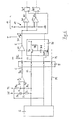
- FIGS 1 to 7 show circuits (or their respective essential parts) of various devices for automatic measuring range adjustment.
- the sensor is marked with S, the device with G and the connector with 5.
- the sensor can either by itself, for. B. be supplied with voltage by its own power supply, or as in all embodiments, via the connector 5 from the device. Every single socket and every single plug of the connector is called "plug element St ". Ri always denotes the internal resistance of the device, Re the detection resistance of the sensor.
- a line carrying the measurement signal is always designated M, regardless of whether it belongs to the sensor or the device and whether it carries an unamplified or already amplified measurement signal. Instead of the only one shown everywhere, there can be two parallel detection lines. All sections of a line coming from the detection resistor Re are always labeled E, regardless of whether they are present on the sensor side, device side, before or after an amplifier.
- the sensor is supplied with DC voltage.
- the measurement signal line M from the sensor leads via a plug element St3 to the input of an amplifier V arranged in the device G, the output of which leads to a plug element St4.
- the plug-in elements St4 and St5 are through the bay Resistance bridged.
- a line M, E which is both a measurement signal line and a detection line, leads from the plug element St5 to the device G, the internal resistance Ri of which is shown separately.
- the detection resistor Re can be arranged in the sensor itself or in the sensor plug-in part. The ratio of the resistances Re / Ri is decisive for the adaptation. These two resistors together form a voltage divider 10.
- a tap 9 between the two resistors is the signal input of the device G. (Ri is the internal resistance of the device.)
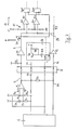
- the connector is shown in simplified form in FIG. 2 and the following figures.
- measurement signal line M and detection line E are separated from one another.
- DC voltage is used for the supply.
- the detection resistor Re arranged on the sensor side and the internal resistance Ri of the device form a voltage divider 10.
- the detection resistor Re leads from the positive pole of the voltage supply via plug elements St1 to the tap 9 of the voltage divider. This tap is connected to the input of an amplifier V1.
- the amplifier output leads to a stage comparator, which is designated as a whole by 11 and has a digital, in particular decimal output.
- the right end of the detection line E is connected to the one input of a series of comparators K1 to Kn, only two of which are shown here.
- the other inputs of these comparators are located at the junctures between the individual resistors (there are more resistors than shown) of a voltage part 12 which bridges the voltage source.
- output signals can appear at one or more of the comparators In the case of simple comparators, either none, some of the comparators or all of them. If window comparators are used, an output signal only occurs at a selected comparator, namely only at the one at which the input voltage difference falls within a certain range, the "window".
- the outputs of the comparators are connected to the positive pole via a series resistor Rv.
- a light-emitting diode 14 can lie in each of these lines. The LEDs can be used to display the physical quantity to be measured and to display the set measuring range and can each illuminate a window with an inscription such as "pressure", "temperature” etc.
- a relay R11 to Rln is located between the outputs A1 to On and ground. When using window comparators, only one of these relays is turned on, and this case will be used for the further description.
- the measurement signal line contains an amplifier V2 on the device side and then a voltage divider 15 with a tap 17 which is connected to the positive input of the device G. Between this tap and the output of the amplifier V2 there is a series resistor Rm (the measurement signal line) which forms one branch of the voltage divider 15.
- the ratios R1 / Rm to Rn / Rm of the resistors are decisive for the adaptation.
- the sensor is supplied with AC voltage.
- a voltage divider 10 is formed which contains the detection resistor Re on the sensor side and the internal resistance Ri of the device on the device side. Its tap 9 is fed to the negative input of an operational amplifier Vo.
- the voltage source is bridged by two equally large resistors Rs and Rt, the common connection point of which is connected to the positive input of the operational amplifier Vo.
- a feedback resistor Rr leads to its signal input in the usual way.
- H. tap 9 The output signal of the operational amplifier is rectified by a diode D1 with capacitor C1. The rectified signal is fed to an amplifier V1 and its output signal in turn to a stage comparator. The rest of the circuit and its mode of operation are the same as shown in FIG. 2 and described with reference to FIG.
- the resistors shown in FIG. 3 need not be ohmic resistors, but can be very generally impedances and contain capacitors, coils and / or semiconductors.
- the sensor S is supplied with direct voltage.
- the adaptation can be achieved via coding and decoding.
- a number of z. B. eight coding switches Sk1, Sk2 to Skn are provided, which are all connected to the positive pole. The other side of each of the switches leads to one of the plug elements St1 to Stn.
- Device egg A binary decimal decoder 16 is provided which has n inputs. Depending on which of the switches Sk1 to Skn are closed, a signal is present at one of the decimal outputs A1 to Am. As described with reference to FIG. 2, one of the matching resistors R1 to Rn of the device is accordingly switched on. The measurement signal is fed to the device as described with reference to FIG. 2.
- the ratio of two detection resistors Re1 and Re2 can be encoded.
- the resistance ratio can then only be determined briefly, in particular when the sensor is plugged in or when the voltage supply is switched on.
- the detection line E can be grounded between the connector 5 and the amplifier V1 by a changeover switch Sx.
- the switch can be closed by a monostable multivibrator (Monoflop Mf1 "Power Reset") for a short time.
- the Monoflop Mf1 can be started either manually or automatically or after applying the supply voltage. It returns after a pulse (the first switching time) of z. B.
- a tap 22 is connected to ground between the two detection resistors Re1 and Re2.
- the upper side of the semiconductor circuit 20 in FIG. 5 is connected to plus.
- a transistor T1 now becomes conductive via the resistor Re2, a resistor R4 and a capacitor C1.
- the transistor T2 becomes conductive via a resistor R5 which is connected to the collector of this transistor and the base of a transistor T2. From now on, the capacitor C1 is charged.
- the detection is connected in series resistances Re1 and Re2 approximately at the full supply voltage.
- a signal appears in the detection line E, the voltage of which is given by the ratio of the two detection resistors.
- the amplifier V1 After passing through the amplifier V1, it is evaluated in the manner described below, and thus serves to set one of the matching resistors R1 to Rn (FIG. 2) for the device.
- the changeover switch Sx is brought back into its drawn position by the monaflop Mf1, which on the one hand separates the tap 22 from the ground and on the other hand starts a monoflop Mf2 which has a dynamic or clock input. Its output is connected to a dynamic input from memories Sp1 to Spn. A further input of the memory provided for a useful signal is connected to the output of one of the comparators K1 to Kn.
- the monoflop Mf2 remains during a second switching time of e.g. B. active for half a second and activates the memory Sp1 to Spn during this time. As a result, these memories take over the output signal or the output signals which occur at the outputs A1 to An of the comparators K1 to Kn.
- the signals occurring at the outputs of the memories are used in the manner described with reference to FIG. 2 to switch on one of the matching resistors R1 to Rn.
- Detecting the ratio of the detection resistors Rel / Re2 is therefore only possible as long as the capacitor C1 contains a charge. It is therefore not possible to measure the resistance ratio from the outside without a device with a suitable interrogation circuit.
- the value of the detection resistor Re cannot normally be determined from the outside.
- the input Eg1 of a comparator K is normally at a lower potential than its input Eg2. Therefore, no signal occurs at the output of the comparator K and also in the detection line E.
- One input Eg1 of the comparator K is connected to a tap 21 of a series circuit 34 composed of two identical resistors Ra and Rb, the other ends of which are connected to the two poles of the voltage source (supply line VL and ground).
- the second input (Eg2) of the comparator is connected to a tap 23 of a series circuit 35 comprising a reference diode 24 and a resistor Rc. The outer ends of this series circuit 35 are also connected to the supply voltage.
- the reference voltage of the reference diode is dimensioned such that there is normally a higher potential at the Eg2 input than at the Eg1 input, so that the comparator does not normally emit an output signal.
- the circuit is activated by briefly increasing the supply voltage.
- a voltage stabilizer 26 with a transistor T8, a resistor R8 and a Zener diode D8 is used for this purpose.
- the switch can be opened briefly by hand or when the device is switched on and then ensures a definite voltage change at the output of the voltage stabilizer 26 in the line VL. With the switch Sa8 open, the zener diode can no longer work.
- This voltage change briefly increases the potential at input Eg1 of comparator K. It becomes higher than that at the input Eg2, and a detection signal thus occurs at the output of the comparator and after the detection resistor Re in the detection line E, which makes it possible to determine the ratio of the detection resistance Re to the internal resistance Ri.
- a button 30 achieves two things simultaneously when the device and sensor are switched on. On the one hand, switch S8 briefly generates an overvoltage in voltage constant holder 26. On the other hand, when the button 30 is closed, a pulse is given to the clock input of each of the memories, so that the memories are briefly activated.
- the detection signal is again fed to a stage comparator 11, as was described above with reference to FIG. 2.
- One or more output signals of the stage comparator are stored in the memories Sp1 to Spn and, as described, serve to switch on one of the matching resistors R1 to Rn for the device.
- the detection resistance Re has a different position here. It establishes a connection from the output of the comparator K to the measurement signal line M. After an amplifier V2 for the measurement signal and the detection signal, a line 28 leads to the input of the stage comparator 11. Otherwise, this circuit operates like that according to FIG. 6.
Abstract
Description
Die Erfindung bezieht sich auf eine Vorrichtung zur automatischen Anpassung des Meßbereichs eines Anzeige- oder Auswertgerätes (im Folgenden einfach "Gerät" genannt) an den Bereich von Ausgangsspannungen eines Sensors für eine physikalische Größe. Die zu messende physikalische Größe kann beliebig sein, z. B. ein Druck, eine Temperatur, ein pH-Wart oder irgendeine elektrische Größe. Während ein Anzeigegerät lediglich die zu messende Größe, z. B. durch einen Zeigerausschlag oder durch eine Digitalanzeige anzeigt, soll ein Auswertgerät (mit oder ohne Anzeige) als Antwort auf ein ihm eingegebenes Meßsignal irgendetuas bewerkstelligen, z. B. ein Alarmsignal auslösen oder eine Schaltung aktivieren, die ihrerseits beliebige Aufgaben zu erfüllen haben kann. Einem bestimmten Bereich von Spannungen, in den ein vom Sensor abgegebenes Signal (das Meßsignal) fällt, muß z. B. ein Anzeigegegerät so angepaßt werden, daß es einerseits nicht überlastet wird, andererseits seine Anzeige aber gut ablesbar ist. Entsprechendes gilt für ein Auswertgerät.The invention relates to a device for automatically adapting the measuring range of a display or evaluation device (hereinafter simply called "device") to the range of output voltages of a sensor for a physical variable. The physical quantity to be measured can be arbitrary, e.g. B. a pressure, a temperature, a pH-Wart or any electrical quantity. While a display device only the size to be measured, e.g. B. indicates by a pointer deflection or by a digital display, an evaluation device (with or without a display) in response to a measurement signal entered him to accomplish something, z. B. trigger an alarm signal or activate a circuit that in turn can have any task. A certain range of voltages, in which a signal emitted by the sensor (the measurement signal) falls, z. B. a display device can be adjusted so that it is not overloaded on the one hand, but on the other hand its display is easy to read. The same applies to an evaluation device.
Wird nur ein bestimmter Sensor mit einem bestimmten Gerät verwendet, so ist die Anpassung kein Problem. Anders liegt der Fall, wenn verschiedenartige Sensoren benutzt werden sollen, die Meßsignale sehr unterschiedlicher Größen abgeben und wenn alle wechselweise mit demselben Gerät verbunden werden sollen oder wenn derselbe Sensor wechselweise mit dem einen oder anderen Gerät verbunden werden soll und dergleichen Varianten mehr.If only a certain sensor is used with a certain device, the adaptation is not a problem. The situation is different if different types of sensors are to be used, which emit measurement signals of very different sizes and if all are to be connected alternately to the same device or if the same sensor is to be connected alternately to one or the other device and similar variants more.
Durch die vorliegende Erfindung soll die erforderliche Anpassung automatisch beim Anschließen eines Sensors an ein Gerät durchgeführt werden. Diese Aufgabe wird durch die Erfindung nach Anspruch 1 gelöst.The present invention is intended to automatically carry out the required adaptation when a sensor is connected to a device. This object is achieved by the invention according to
Das Folgende bezieht sich auch auf die Uortlaute der Ansprüche.The following also relates to the preamble to the claims.
Erfindungsgemäß wird zum Anschluß des Sensors an das Gerät ein Steckverbinder verwendet. Jedes der in Frage kommenden Geräte ist mit dem einen Teil (z. B. mit Steckstiften) des Steckverbinders versehen, während jeder der Sensoren mit dem anderen Teil (z. B. mit Steckbuchsen) des Steckverbinders versehen ist. Somit kann jeder der Sensoren an jedes der Geräte angeschlossen werden.According to the invention, a connector is used to connect the sensor to the device. Each of the devices in question is provided with one part (e.g. with pins) of the connector, while each of the sensors is provided with the other part (e.g. with sockets) of the connector. Each of the sensors can thus be connected to each of the devices.
Zur automatischen Anpassung dienen der sensorseitig angeordnete Erkennungswiderstand und die geräteseitig angeordnete Erkennungsschaltung, die erst nach dem Anschließen eines Gerätes an einen Sensor wirksam wird.The detection resistor arranged on the sensor side and the detection circuit arranged on the device side are used for the automatic adaptation and only take effect after a device has been connected to a sensor.
Nach Anspruch 2 läßt sich eine Anpassung unter Verwendung einer Reihenschaltung aus zwei Abschnitten bewerkstelligen.According to claim 2, an adaptation can be accomplished using a series connection of two sections.
Der eine Abschnitt entspricht dem Innenwiderstand des Gerätes oder ist gleich diesem Innenwiderstand, der andere, der dem Sensor zugeordnet ist, entspricht einem Erkennungswiderstand oder ist gleich dem Erkennungswiderstand. Dieser Erkennungswiderstand hat für jeden Sensor eine bestimmte typische Größe. Im einfachsten Falle, wenn nämlich alle in Frage kommenden Geräte gleichen Innenwiderstand haben, wird durch die Größe des Erkennungswiderstandes selbst für die richtige Anpassung gesorgt. Hier kann mit einer einfachen Anordnung nach Anspruch 3 gearbeitet werden, bei der die Meßsignalleitung zugleich Erkennungsleitung ist.One section corresponds to the internal resistance of the device or is equal to this internal resistance, the other, which is assigned to the sensor, corresponds to a detection resistance or is equal to the detection resistance. This detection resistor has a certain typical size for each sensor. In the simplest case, when all the devices in question have the same internal resistance, the size of the detection resistance itself ensures the correct adjustment. Here you can work with a simple arrangement according to claim 3, in which the measurement signal line is also the detection line.
In komplizierteren Fällen kann die Größe des Erkennungsuiderstandes nach dem Anschließen des Sensors vom Gerät her ermittelt werden. Vorzugsweise wird dann eine von der Meßsignalleitung unabhängige Erkennungsleitung verwendet. Passend zum Innenwiderstand des Gerätes kann nach Anspruch 5 einer von mehreren Anpaßwiderständen eingeschaltet werden, die z. B. als Shunts parallel zum Eingang des Gerätes geschaltet sind.In more complicated cases, the size of the detection resistance can be determined from the device after connecting the sensor. A detection line which is independent of the measurement signal line is then preferably used. Matching the internal resistance of the device can be turned on according to
Zur Einschaltung des geeigneten Anpaßwiderstandes kann nach Anspruch 6 ein Stufenkomparator verwendet werden, der an die Erkennungsleitung angeschlossen ist.To switch on the suitable matching resistor, a step comparator can be used according to claim 6, which is connected to the detection line.
Nach den Ansprüchen 9 und 10 läßt sich die Erkennung des verwendeten Sensors für den Fall durchführen, daß Sensor und Gerät mit Wechselstrom betrieben werden.According to
Es kann erwünscht sein, die Größe des Erkennungswiderstandes eines Sensors zu verschlüsseln, so daß seine Größe von außen mit normalen Mitteln nicht gemessen werden kann. Solche Maßnahmen haben für Hersteller Bedeutung, die wünschen, daß nur von ihnen selbst hergestellte Sensoren und Geräte verwendet werden, dagegen nicht z. B. Sensoren von fremden Firmen zu eigenen Geräten. Eine Verschlüsselung läßt sich nach Anspruch 11 erreichen, wobei eine aktivierbare Halbleiterschaltung dafür sorgt, daß das Größenverhältnis der hier verwendeten beiden Erkennungswiderstände nur für einen sehr kurzen Zeitraum nach dem Zusammenstecken von Gerät und Sensor festgestellt und dadurch das Gerät angepaßt werden kann. Geräteseitig werden hierbei am Ausgang eines Stufenkomparators dynamische Speicher verwendet, die ebenfalls nur kurzzeitig ein Signal zum Einstellen des geeigneten Anpassungsuiderstandes abgeben.It may be desirable to encode the size of a sensor's detection resistance so that its size cannot be measured from the outside by normal means. Such measures are important for manufacturers who wish that only sensors and devices that they have produced themselves are used. B. Sensors from other companies to own devices. Encryption can be achieved according to
Nach Anspruch 14 läßt sich eine Verschlüsselung auf andere Weise erreichen. Hier wird von einem sensorseitigen Komparator normalerweise kein Ausgangssignal über einen Erkennungsuiderstand abgegeben, sondern erst, wenn Potentiale an seinen Eingängen geändert uerden. Dies kann von einem geräteseitig angeordneten Spannungskonstanthalter her geschehen, der als Spannungsquelle für den Sensor dient und dessen Ausgangsspannung kurz nach dem Einschalten einen anderen, insbesonderen höheren Wert annimmt. Durch diesen höheren Wert werdan die Potentiale an den Eingängen des Komparators im Sensor so geändert, daß der Komparator kurzzeitig ein Ausgangssignal über den Erkennungsuiderstand in die Erkennungsleitung gibt.According to claim 14, encryption can be achieved in a different way. In this case, a comparator on the sensor side normally does not emit an output signal via a detection resistor, but only when potentials at its inputs are changed. This can be from a voltage stabilizer arranged on the device side, which serves as a voltage source for the sensor and whose output voltage assumes a different, in particular higher, value shortly after switching on. This higher value changes the potentials at the inputs of the comparator in the sensor so that the comparator briefly outputs an output signal via the detection resistor into the detection line.
Nach Anspruch 16 läßt sich eine verschlüsselte Anpassung ohne Erkennungswiderstand in der Weise durchführen, daß sensorseitig einige, insbesondere binäre, Kodierungsschalter vorgesehen sind und geräteseitig ein Dekoder, insbesondere ein Binär-Dezimal-Dekoder, der dann für die Einstellung des geeigneten Anpassungsuiderstandes sorgt. Ausführungsbeispiele mit weiteren Merkmalen der Erfindung werden im folgenden anhand der Zeichnungen beschrieben.According to
Die Figuren 1 bis 7 zeigen Schaltungen (oder deren jeweils wesentliche Teile) verschiedener Vorrichtungen zur automatischen Meßbereichs-Anpassung.Figures 1 to 7 show circuits (or their respective essential parts) of various devices for automatic measuring range adjustment.
Der Sensor ist mit S, das Gerät mit G und der Steckverbinder mit 5 bezeichnet. Der Sensor kann entweder für sich, z. B. durch ein eigenes Netzteil mit Spannung versorgt werden, oder wie in allen Ausführungsbeispielen, über den Steckverbinder 5 vom Gerät her. Jede einzelne Buchse und jeder einzelne Stecker des Steckverbinders werden als "Steckelement St..." bezeichnet. Mit Ri ist immer der Innenwiderstand des Gerätes bezeichnet, mit Re der Erkennungsuiderstand des Sensors.The sensor is marked with S, the device with G and the connector with 5. The sensor can either by itself, for. B. be supplied with voltage by its own power supply, or as in all embodiments, via the
Eine das Meßsignal führende Leitung ist stets mit M bezeichnet, gleichgültig, ob sie zum Sensor oder zum Gerät gehört und ob sie ein unverstärktes oder schon verstärktes Meßsignal führt. Anstelle der überall dargestellten einzigen können zwei parallele Erkennungsleitungen vorhanden sein. Alle Abschnitte einer vom Erkennungswiderstand Re herkommenden Leitung sind immer mit E bezeichnet, gleichgültig ob sie sensorseitig, geräteseitig, vor oder nach einem Verstärker vorhanden sind.A line carrying the measurement signal is always designated M, regardless of whether it belongs to the sensor or the device and whether it carries an unamplified or already amplified measurement signal. Instead of the only one shown everywhere, there can be two parallel detection lines. All sections of a line coming from the detection resistor Re are always labeled E, regardless of whether they are present on the sensor side, device side, before or after an amplifier.
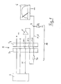
Der Sensor wird mit Gleichspannung versorgt. Die Meßsignalleitung M vom Sensor führt über ein Steckelement St3 zum Eingang eines im Gerät G angeordneten Verstärkers V, dessen Ausgang zu einem Steckelement St4 führt. Sensorseitig sind die Steckelemente St4 und St5 durch den Erkennungsuiderstand Re überbrückt. Geräteseitig führt vom Steckelement St5 eine Leitung M, E, die sowohl Meßsignalleitung als auch Erkennungsleitung ist, zum Gerät G, dessen Innenwiderstand Ri gesondert eingezeichnet ist. Vorausgesetzt, daß nur Geräte verwendet werden, die gleiche Innenwiderstände und gleiche Anzeigebereiche haben, genügt diese Schaltung, um Sensoren verschiedener Art diesen Geräten anzupassen. Der Erkennungswiderstand Re kann im Sensor selbst oder im Sensorsteckteil angeordnet sein. Maßgebend für die Anpassung ist das Verhältnis der Widerstände Re/Ri. Diese beiden Widerstände bilden gemeinsam einen Spannungsteiler 10. Ein Abgriff 9 zwischen beiden Widerständen ist der Signaleingang des Gerätes G. (Ri ist der Innenwiderstand des Gerätes.)The sensor is supplied with DC voltage. The measurement signal line M from the sensor leads via a plug element St3 to the input of an amplifier V arranged in the device G, the output of which leads to a plug element St4. On the sensor side, the plug-in elements St4 and St5 are through the bay Resistance bridged. On the device side, a line M, E, which is both a measurement signal line and a detection line, leads from the plug element St5 to the device G, the internal resistance Ri of which is shown separately. Provided that only devices are used that have the same internal resistances and the same display areas, this circuit is sufficient to adapt sensors of different types to these devices. The detection resistor Re can be arranged in the sensor itself or in the sensor plug-in part. The ratio of the resistances Re / Ri is decisive for the adaptation. These two resistors together form a
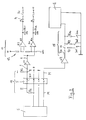
In Figur 2 und den folgenden Figuren ist der Steckverbinder vereinfacht dargestellt. Nach Figur 2 sind Meßsignalleitung M und Erkennungsleitung E voneinander getrennt. Zur Versorgung dient wiederum Gleichspannung. Wiederum bilden der sensorseitig angeordnete Erkennungsuiderstand Re und der Innenwiderstand Ri des Gerätes einen Spannungsteiler 10. Der Erkennungsuiderstand Re führt vom Pluspol der Spannungsversorgung über Steckelemente St1 zum Abgriff 9 des Spannungsteilers. Dieser Abgriff ist mit dem Eingang eines Verstärkers V1 verbunden. Der Verstärkerausgang führt zu einem Stufenkomparator, der als ganzes mit 11 bezeichnet ist und einen digitalen, insbesondere dezimalen Ausgang hat. Das rechte Ende der Erkennungsleitung E ist mit dem einen Eingang einer Reihe von Komparatoren K1 bis Kn verbunden, von denen hier nur zwei dargestellt sind. Die anderen Eingänge dieser Komparatoren liegen an den Verbindungsstellen zwischen den einzelnen Widerständen (es sind mehr Widerstände als dargestellt) eines Spannungsteiles 12, der die Spannungsquelle überbrückt.The connector is shown in simplified form in FIG. 2 and the following figures. According to FIG. 2, measurement signal line M and detection line E are separated from one another. DC voltage is used for the supply. Again, the detection resistor Re arranged on the sensor side and the internal resistance Ri of the device form a
Je nach der Größe des den Verstärker V1 verlassenden Erkennungssignals können an einem oder mehreren der Komparatoren Ausgangssignale auftreten. Bei einfachen Komparatoren entweder an keinem, an einem Teil der Komparatoren oder an allen. Werden Fensterkomparatoren verwendet, so tritt nur an einem ausgewählten Komparator ein Ausgangssignal auf, nämlich nur an demjenigen, bei dem die Eingangs-Spannungsdifferenz in einen bestimmten Bereich, das "Fenster" fällt. Die Ausgänge der Komparatoren liegen über je einen Reihenwiderstand Rv am Pluspol. In diesen Leitungen kann je eine Leuchtdiode 14 liegen. Die Leuchtdioden können zur Anzeige der zu messenden physikalischen Größe und zur Anzeige des eingestellten Meßbereiches verwendet werden und können je ein Fenster mit einer Aufschrift wie "Druck", "Temperatur" usw. erleuchten.Depending on the size of the detection signal leaving the amplifier V1, output signals can appear at one or more of the comparators In the case of simple comparators, either none, some of the comparators or all of them. If window comparators are used, an output signal only occurs at a selected comparator, namely only at the one at which the input voltage difference falls within a certain range, the "window". The outputs of the comparators are connected to the positive pole via a series resistor Rv. A light-emitting diode 14 can lie in each of these lines. The LEDs can be used to display the physical quantity to be measured and to display the set measuring range and can each illuminate a window with an inscription such as "pressure", "temperature" etc.
Zwischen den Ausgängen A1 bis An und Masse liegt je ein Relais R11 bis Rln. Bei Verwendung von Fensterkomparatoren wird nur eines dieser Relais eingeschaltet, und dieser Fall wird für die weitere Beschreibung zugrunde gelegt.A relay R11 to Rln is located between the outputs A1 to On and ground. When using window comparators, only one of these relays is turned on, and this case will be used for the further description.
Die Meßsignalleitung enthält geräteseitig einen Verstärker V2 und anschließend einen Spannungsteiler 15 mit einem Abgriff 17, der mit dem positiven Eingang des Gerätes G verbunden ist. Zwischen diesem Abgriff und dem Ausgang des Verstärkers V2 liegt ein Reihenwiderstand Rm (der Meßsignalleitung), der den einen Zweig des Spannungsteilers 15 bildet. Den anderen Zweig des Spannungsteilers 15, der den Eingang des Gerätes G überbrückt, bildet eine Gruppe zueinander paralleler Reihenglieder, die je einen Widerstand (Anpaßuiderstand) R1 bis Rn und einen Analogschalter Sa1 bis San enthalten. Diese Schalter sind durch die Relais R11 bis Rln wahlweise zu betätigen. Je nachdem, welcher Komparator anspricht, wird einer der Anpaßwiderstände R1 bis Rn eingeschaltet. Er überbrückt als Shunt den Eingang des Gerätes und stellt damit den erforderlichen Meßbereich ein. Für die Anpassung sind die Verhältnisse R1/Rm bis Rn/Rm der Widerstände maßgebend.The measurement signal line contains an amplifier V2 on the device side and then a
Uas hier der Einfachheit halber als Relaisschaltung dargestellt wurde, läßt sich eleganter unter Verwendung von Halbleiterschaltern durchführen, wodurch Schaltkontakte vermieden werden.What has been shown here as a relay circuit for the sake of simplicity can be carried out more elegantly using semiconductor switches, as a result of which switching contacts are avoided.
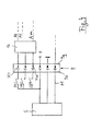
Bei dem Ausführungsbeispiel nach Figur 3 wird der Sensor mit Wechselspannung versorgt. Es wird wiederum ein Spannungsteiler 10 gebildet, der sensorseitig den Erkennungswiderstand Re und geräteseitig den Innenwiderstand Ri des Gerätes enthält. Sein Abgriff 9 wird dem negativen Eingang eines Operationsverstärkers Vo zugeführt. Um für den anderen Eingang dieses Operationsverstärkers eine definierte Spannung zu haben, wird die Spannungsquelle durch zwei gleich große Widerstände Rs und Rt überbrückt, deren gemeinsame Verbindungsstelle mit dem positiven Eingang des Operationsverstärkers Vo verbunden ist. Vom Ausgang des Operationsverstärkers führt in üblicher Weise ein Rückkopplungswiderstand Rr zu seinem Signaleingang, d. h. zum Abgriff 9. Das Ausgangssignal des Operationsverstärkers wird durch eine Diode D1 mit Kondensator C1 gleichgerichtet. Das gleichgerichtete Signal wird einem Verstärker V1 zugeführt und dessen Ausgangsignal wiederum einem Stufenkomparator. Die übrige Schaltung und ihre Wirkungsweise sind die gleichen wie in Figur 2 dargestellt und anhand der Figur 2 beschrieben.In the embodiment of Figure 3, the sensor is supplied with AC voltage. In turn, a
Die in Figur 3 dargestellten Widerstände brauchen keine ohmschen Widerstände zu sein, sondern können ganz allgemein Impedanzen sein und Kondensatoren, Spulen und/oder Halbleiter enthalten.The resistors shown in FIG. 3 need not be ohmic resistors, but can be very generally impedances and contain capacitors, coils and / or semiconductors.
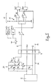
Bei dem Ausführungsbeispiel nach Figur 4 wie auch bei den folgenden wird der Sensor S mit Gleichspannung versorgt. Nach Figur 4 läßt sich die Anpassung über eine Kodierung und Dekodierung erzielen. Sensorseitig ist eine Reihe von z. B. acht Kodierungsschaltern Sk1, Sk2 bis Skn vorgesehen, die alle mit dem Pluspol verbunden sind. Die andere Seite jedes der Schalter führt zu je einem der Steckelemente St1 bis Stn. Geräteseitig ist ein Binär-Dezimal-Dekoder 16 vorgesehen, der entsprechend n Eingänge hat. Je nachdem, welche der Schalter Sk1 bis Skn geschlossen sind, steht an einem der dezimalen Ausgänge A1 bis Am ein Signal an. Wie anhand der Figur 2 beschrieben, wird dementsprechend einer der Anpaßwiderstände R1 bis Rn des Gerätes eingeschaltet. Das Meßsignal wird dem Gerät zugeführt, wie anhand der Figur 2 beschrieben.In the exemplary embodiment according to FIG. 4 as well as in the following, the sensor S is supplied with direct voltage. According to FIG. 4, the adaptation can be achieved via coding and decoding. A number of z. B. eight coding switches Sk1, Sk2 to Skn are provided, which are all connected to the positive pole. The other side of each of the switches leads to one of the plug elements St1 to Stn. Device egg A binary
Nach Figur 5 läßt sich das Verhältnis zweier Erkennungsuiderstände Re1 und Re2 verschlüsseln. Das Uiderstandsverhältnis kann dann nur kurzzeitig, insbesondere beim Einstecken des Sensors oder beim Einschalten der Spannungsversorgung ermittelt uerden. Hierzu ist u. a. eine aktivierbare Halbleiterschaltung vorgesehen, die als Ganzes mit 20 bezeichnet ist. Die Erkennungsleitung E läßt sich zwischen dem Steckverbinder 5 und dem Verstärker V1 durch einen Umschalter Sx an Masse legen. Der Umschalter läßt sich durch einen monostabilen Multivibrator (Monoflop Mf1 "Power Reset") für kurze Zeit schließen. Das Monoflop Mf1 kann entweder auf Anforderung von Hand oder automatisch oder nach Anlegen der Versorgungsspannung gestartet werden. Es kehrt nach Ablauf eines Impulses (der ersten Schaltzeit) von z. B. 10 msec Dauer wieder in seinen Urzustand zurück, in dem er die Erkennungsleitung E wieder von Masse getrennt hält. Während der ersten Schaltzeit liegt ein Abgriff 22 zwischen den beiden Erkennungswiderständen Re1 und Re2 an Masse. Die in Figur 5 obere Seite der Halbleiterschaltung 20 liegt an plus. Es wird nun über den Widerstand Re2, einen Widerstand R4 und einen Kondensator C1 ein Transistor T1 leitend. Hierdurch wird über einen Widerstand R5, der mit dem Kollektor dieses Transistors und der Basis eines Transistors T2 verbunden ist, der Transistor T2 leitend. Von nun an wird der Kondensator C1 aufgeladen.According to FIG. 5, the ratio of two detection resistors Re1 and Re2 can be encoded. The resistance ratio can then only be determined briefly, in particular when the sensor is plugged in or when the voltage supply is switched on. This is u. a. an activatable semiconductor circuit is provided, which is designated as a whole by 20. The detection line E can be grounded between the
Während dieses Ladevorganges (und danach, solange der Kondensator eine nennenswerte Ladung enthält) liegt die Reihenschaltung der Erkennungswiderstände Re1 und Re2 annähernd an der vollen Versorgungsspannung. Infolgedessen tritt in der Erkennungsleitung E ein Signal auf, dessen Spannung durch das Verhältnis der beiden Erkennungswiderstände gegeben ist. Es wird nach Durchlaufen des Verstärkers V1 in der weiter unten beschriebenen Weise ausgewertet, dient also zum Einstellen eines der Anpaßwiderstände R1 bis Rn (Figur 2) für das Gerät.During this charging process (and after that, as long as the capacitor contains a significant charge), the detection is connected in series resistances Re1 and Re2 approximately at the full supply voltage. As a result, a signal appears in the detection line E, the voltage of which is given by the ratio of the two detection resistors. After passing through the amplifier V1, it is evaluated in the manner described below, and thus serves to set one of the matching resistors R1 to Rn (FIG. 2) for the device.
Nach Ablauf der ersten Schaltzeit wird vom Monaflop Mf1 her der Umschalter Sx wieder in seine eingezeichnete Stellung gebracht, wodurch einerseits der Abgriff 22 von Masse getrennt und andererseits ein Monoflop Mf2 gestartet wird, das einen dynamischen oder Clock-Eingang hat. Sein Ausgang ist mit je einem dynamischen Eingang von Speichern Sp1 bis Spn verbunden. Je ein weiterer für ein Nutzsignal vorgesehener Eingang der Speicher ist mit dem Ausgang eines der Komparatoren K1 bis Kn verbunden.After the first switching time has elapsed, the changeover switch Sx is brought back into its drawn position by the monaflop Mf1, which on the one hand separates the
Das Monoflop Mf2 bleibt während einer zweiten Schaltzeit von z. B. einer halben Sekunde aktiv und aktiviert während dieser Zeit die Speicher Sp1 bis Spn. Dadurch übernehmen diese Speicher das Ausgangssignal oder die Ausgangssignale, die an den Ausgängen A1 bis An der Komperatoren K1 bis Kn auftreten.The monoflop Mf2 remains during a second switching time of e.g. B. active for half a second and activates the memory Sp1 to Spn during this time. As a result, these memories take over the output signal or the output signals which occur at the outputs A1 to An of the comparators K1 to Kn.
Die an den Ausgängen der Speicher auftretenden Signale werden in der anhand der Figur 2 beschriebenen Weise zum Einschalten eines der Anpaßwiderstände R1 bis Rn verwendet.The signals occurring at the outputs of the memories are used in the manner described with reference to FIG. 2 to switch on one of the matching resistors R1 to Rn.
Ein Erkennen des Verhältnisses der Erkennungswiderstände Rel/Re2 ist also nur möglich, solange der Kondensator C1 eine Ladung enthält. Es ist daher nicht möglich, ohne ein Gerät mit passender Abfrageschaltung von außen her das Widerstandsverhältnis zu messen.Detecting the ratio of the detection resistors Rel / Re2 is therefore only possible as long as the capacitor C1 contains a charge. It is therefore not possible to measure the resistance ratio from the outside without a device with a suitable interrogation circuit.
Auch bei der Schaltung nach Figur 6 läßt sich der Wert des Erkennungswiderstandes Re normalerweise von außen her nicht feststellen. Normalerweise liegt der Eingang Eg1 eines Komparators K auf einem niedrigeren Potential als dessen Eingang Eg2. Deshalb tritt am Ausgang des Komparators K und ebenso in der Erkennungsleitung E kein Signal auf.Also in the circuit according to FIG. 6, the value of the detection resistor Re cannot normally be determined from the outside. The input Eg1 of a comparator K is normally at a lower potential than its input Eg2. Therefore, no signal occurs at the output of the comparator K and also in the detection line E.
Der eine Eingang Eg1 des Komparators K liegt an einem Abgriff 21 einer Reihenschaltung 34 aus zwei gleich großen Widerständen Ra und Rb, deren andere Enden an den beiden Polen der Spannungsquelle (Versorgungsleitung VL und Masse) liegen. Der zweite Eingang (Eg2) des Komparators liegt an einem Abgriff 23 einer Reihenschaltung 35 aus einer Referenzdiode 24 und einem Widerstand Rc. Die äußeren Enden dieser Reihenschaltung 35 liegen ebenfalls an der Versorgungsspannung. Die Bezugsspannung der Referenzdiode ist so bemessen, daß am Eingang Eg2 normalerweise ein höheres Potential als am Eingang Eg1 liegt, so daß der Komparator normalerweise kein Ausgangssignal abgibt.One input Eg1 of the comparator K is connected to a
Die Schaltung wird dadurch aktiviert, daß die Versorgungsspannung kurzzeitig erhöht wird. Hierzu dient ein Spannungskonstanthalter 26 mit einem Transistor T8, einem Widerstand R8 und einer Zenerdiode D8. Zwischen der Zenerdiode und Masse liegt ein Schalter (Öffner) Sa8. Der Schalter kann von Hand oder beim Einschalten des Gerätes kurzzeitig geöffnet werden und sorgt dann für eine definitive Spannungsänderung am Ausgang des Spannungs-Konstanthalters 26 in der Leitung VL. Bei offenem Schalter Sa8 kann nämlich die Zenerdiode nicht mehr arbeiten. Durch diese Spannungsänderung wird das Potential am Eingang Eg1 des Komparators K kurzzeitig erhöht. Es wird höher als das am Eingang Eg2, und damit tritt am Ausgang des Komparators und nach dem Erkennungswiderstand Re in der Erkennungsleitung E ein Erkennungssignal auf, das es ermöglicht, das Verhältnis des Erkennungsuiderstandes Re zum Innenwiderstand Ri festzustellen.The circuit is activated by briefly increasing the supply voltage. A
Durch einen Taster 30 wird beim Einschalten von Gerät und Sensor zweierlei gleichzeitig erreicht. Einerseits wird vom Schalter S8 im Spannungs- konstanthalter 26 kurzzeitig eine Überspannung erzeugt. Andererseits wird beim Schließen des Tasters 30 je ein Impuls auf den Clock-Eingang jedes der Speicher gegeben, so daß die Speicher kurzzeitig aktiviert werden.A
Wie der Schalter S8 im einzelnen betätigt wird, ist dem Fachmann bekannt und hier nur durch eine gestrichtelte Verbindung 32 dargestellt.How the switch S8 is actuated in detail is known to the person skilled in the art and is shown here only by a dashed connection 32.
Nach Verstärkung im Verstärker V1 wird das Erkennungssignal wiederum einem Stufenkomparator 11 zugeführt, wie es oben anhand der Figur 2 beschrieben wurde. Eines oder mehrere Ausgangssignale des Stufenkomparators werden in den Speichern Sp1 bis Spn gespeichert und dienen, wie beschrieben, zum Einschalten eines der Anpaßwiderstände R1 bis Rn für das Gerät.After amplification in the amplifier V1, the detection signal is again fed to a
Wie Figur 7 zeigt, hat der Erkennungswiderstand Re hier eine andere Lage. Er stellt nämlich eine Verbindung vom Ausgang des Komparators K zur Meßsignalleitung M her. Hinter einem Verstärker V2 für das Meßsignal und das Erkennungssignal führt eine Leitung 28 zum Eingang des Stufenkomparators 11. Im übrigen arbeitet diese Schaltung wie die nach Figur 6.As FIG. 7 shows, the detection resistance Re has a different position here. It establishes a connection from the output of the comparator K to the measurement signal line M. After an amplifier V2 for the measurement signal and the detection signal, a
- 5 Steckverbinder5 connectors
- 5s Sensor-Stedcteil5s sensor section
- 5g Geräte-Steckteil5g device plug-in part
- 9 Abgriff9 tap
- 10 Spannungsteiler10 voltage dividers
- 11 Stufenkomparator11 stage comparator
- 12 Spannungsteiler12 voltage dividers
- 14 Leuchtdiode14 light emitting diode
- 15 Spannungsteiler15 voltage dividers
- 16 Dekoder16 decoders
- 17 Abgriff17 tap
- 20 Aktive Halbleiterschaltung20 Active semiconductor circuit
- 21, 22, 23 Abgriff21, 22, 23 tap
- 24 Referenzdiode24 reference diode
- 26 Spannungs-Konstanthalter26 voltage stabilizer
- 28 Leitung28 line
- 30 Taster30 buttons
- 32 Verbindung32 connection
- 34, 35 Reihenschaltung34, 35 series connection
- A... AusgängeA ... exits
- C1 KondensatorC1 capacitor
- D1 DiodeD1 diode
- D8 ZenerdiodeD8 zener diode
- G GerätG device
- E ErkennungsleitungE detection line
- Eg EingangEg entrance
- K... KomparatorenK ... comparators
- Π MeßsignalleitungΠ Measurement signal line
- Mf1, 2 MonoflopMf1, 2 monoflop
- R... Widerstand, AnpaßwiderstandR ... resistance, matching resistance
- Re ErkennungswiderstandRe detection resistance
- Ri InnenwiderstandRi internal resistance
- Rm ReihenwiderstandRm series resistance
- Rr RückkopplungswiderstandRr feedback resistance
- Rs, Rt WiderständeRs, Rt resistors
- Rv ReihenwiderstandRv series resistance
- Rl RelaisRl relay
- S SensorS sensor
- Sa... Schalter, AnalogschalterSa ... switch, analog switch
- Sk... KodierungsschalterSk ... coding switch
- St... SteckelementSt ... plug element
- Sx UmschalterSx switch
- T... TransistorT ... transistor
- V... VerstärkerV ... amplifier
- Vo OperationsverstärkerVo operational amplifier
- VL VersorgungsleitungVL supply line
Claims (16)
(Figur 2)4. The device according to claim 2, characterized by the following features:
(Figure 2)
(Figur 2 und 3)9. Device according to one of claims 2, 5 or 6, characterized by the following features:
(Figure 2 and 3)
(Figur 3)10. The device according to claim 9, characterized by the following features:
(Figure 3)
(Figur 5)12. The apparatus according to claim 11, characterized by the following features:
(Figure 5)
Applications Claiming Priority (2)
| Application Number | Priority Date | Filing Date | Title |
|---|---|---|---|
| DE3524770 | 1985-07-11 | ||
| DE3524770 | 1985-07-11 |
Publications (2)
| Publication Number | Publication Date |
|---|---|
| EP0212045A2 true EP0212045A2 (en) | 1987-03-04 |
| EP0212045A3 EP0212045A3 (en) | 1988-01-27 |
Family
ID=6275501
Family Applications (1)
| Application Number | Title | Priority Date | Filing Date |
|---|---|---|---|
| EP86101552A Withdrawn EP0212045A3 (en) | 1985-07-11 | 1986-02-06 | Adaptation of a display or evaluation device to a sensor |
Country Status (1)
| Country | Link |
|---|---|
| EP (1) | EP0212045A3 (en) |
Cited By (5)
| Publication number | Priority date | Publication date | Assignee | Title |
|---|---|---|---|---|
| DE3826767A1 (en) * | 1988-08-06 | 1990-02-08 | Kostal Leopold Gmbh & Co Kg | Sensor device |
| WO1994008215A1 (en) * | 1992-09-29 | 1994-04-14 | Endress U. Hauser Gmbh U. Co. | Device for determining and/or monitoring a predetermined level of contents of a container |
| EP0607464A1 (en) * | 1992-09-11 | 1994-07-27 | Societe Marechaux Dubost Instruments S.A. | Multifunction measuring acquisition device |
| EP1271167B1 (en) * | 2002-04-06 | 2004-02-18 | Agilent Technologies, Inc. (a Delaware corporation) | Electrical System for testing the channels of a communication system |
| EP1271168B1 (en) * | 2002-04-06 | 2004-12-15 | Agilent Technologies, Inc. (a Delaware corporation) | Electrical system for testing the channels of a communication system |
Citations (3)
| Publication number | Priority date | Publication date | Assignee | Title |
|---|---|---|---|---|
| US3464012A (en) * | 1967-02-17 | 1969-08-26 | Webb James E | Automatic signal range selector for metering devices |
| US3577076A (en) * | 1968-09-05 | 1971-05-04 | Ibm | Automatic range scale selection apparatus for a measuring device |
| US3943440A (en) * | 1974-10-03 | 1976-03-09 | Hewlett-Packard Company | Sensitivity coding circuit for an electronic instrument |
-
1986
- 1986-02-06 EP EP86101552A patent/EP0212045A3/en not_active Withdrawn
Patent Citations (3)
| Publication number | Priority date | Publication date | Assignee | Title |
|---|---|---|---|---|
| US3464012A (en) * | 1967-02-17 | 1969-08-26 | Webb James E | Automatic signal range selector for metering devices |
| US3577076A (en) * | 1968-09-05 | 1971-05-04 | Ibm | Automatic range scale selection apparatus for a measuring device |
| US3943440A (en) * | 1974-10-03 | 1976-03-09 | Hewlett-Packard Company | Sensitivity coding circuit for an electronic instrument |
Cited By (8)
| Publication number | Priority date | Publication date | Assignee | Title |
|---|---|---|---|---|
| DE3826767A1 (en) * | 1988-08-06 | 1990-02-08 | Kostal Leopold Gmbh & Co Kg | Sensor device |
| EP0607464A1 (en) * | 1992-09-11 | 1994-07-27 | Societe Marechaux Dubost Instruments S.A. | Multifunction measuring acquisition device |
| WO1994008215A1 (en) * | 1992-09-29 | 1994-04-14 | Endress U. Hauser Gmbh U. Co. | Device for determining and/or monitoring a predetermined level of contents of a container |
| US5717383A (en) * | 1992-09-29 | 1998-02-10 | Endress + Hauser Gmbh + Co. | Device for determining and/or monitoring a predetermined level of contents in a container |
| EP1271167B1 (en) * | 2002-04-06 | 2004-02-18 | Agilent Technologies, Inc. (a Delaware corporation) | Electrical System for testing the channels of a communication system |
| EP1271168B1 (en) * | 2002-04-06 | 2004-12-15 | Agilent Technologies, Inc. (a Delaware corporation) | Electrical system for testing the channels of a communication system |
| US6844746B2 (en) | 2002-04-06 | 2005-01-18 | Agilent Technologies, Inc. | Electrical system like a testing system for testing the channels of a communication system |
| US7149286B2 (en) | 2002-04-06 | 2006-12-12 | Heinz Nuessle | Electrical system like a system for testing the channels of a communication system |
Also Published As
| Publication number | Publication date |
|---|---|
| EP0212045A3 (en) | 1988-01-27 |
Similar Documents
| Publication | Publication Date | Title |
|---|---|---|
| EP0011711B1 (en) | Test device for the stepwise indication of a measurement voltage | |
| DE2012900A1 (en) | Automatic testing device for multi-core electrical cables | |
| CH619786A5 (en) | ||
| DE2703880B2 (en) | Electrical test device with acoustic, quantitative analog display for resistance and voltage | |
| DE112017004536T5 (en) | MPS generation system and method | |
| DE2809596A1 (en) | Circuit detecting earth faults in two=wire signal line - has resistor connected to each battery terminal and earthed in turns | |
| EP0212045A2 (en) | Adaptation of a display or evaluation device to a sensor | |
| DE2613647A1 (en) | CIRCUIT ARRANGEMENT | |
| EP0052220B1 (en) | Method and device for measuring the resistance in a signalling line | |
| DE19844465A1 (en) | Current measuring circuit arrangement | |
| DE3027398A1 (en) | Electrical indicator deriving power from measurement current - using evaluation circuit consuming less than quiescent current | |
| DE3344363C2 (en) | ||
| DE3915880C2 (en) | ||
| DE2729271A1 (en) | DEVICE FOR PERFORMANCE OF CLASSIFICATION TESTS, IN PARTICULAR COLOR CLASSIFICATION TESTS | |
| DE2607606C2 (en) | Potential tester | |
| DE3701070C2 (en) | ||
| DE3924693C2 (en) | ||
| DE3006011C2 (en) | ||
| DE2364424C2 (en) | Tester for bipolar and field effect transistors | |
| AT397591B (en) | MEASURING DEVICE FOR DETECTING AND DISPLAYING VARIOUS MEASURED VALUES, ESPECIALLY FOR MEASURING VALUES IN NETWORKS OF DIALING SYSTEMS | |
| DE3813883C2 (en) | ||
| DE2060884C3 (en) | Test device for displaying the polarity or the phase position of electrical potentials | |
| AT202385B (en) | Procedure and direction for the statistical control of a quality label according to a group method | |
| DE1513830C3 (en) | ||
| EP0180907B1 (en) | Signalling arrangement in a risk-signalling system |
Legal Events
| Date | Code | Title | Description |
|---|---|---|---|
| PUAI | Public reference made under article 153(3) epc to a published international application that has entered the european phase |
Free format text: ORIGINAL CODE: 0009012 |
|
| AK | Designated contracting states |
Kind code of ref document: A2 Designated state(s): AT CH DE FR GB IT LI NL SE |
|
| PUAL | Search report despatched |
Free format text: ORIGINAL CODE: 0009013 |
|
| RHK1 | Main classification (correction) |
Ipc: G01R 15/08 |
|
| AK | Designated contracting states |
Kind code of ref document: A3 Designated state(s): AT CH DE FR GB IT LI NL SE |
|
| 17P | Request for examination filed |
Effective date: 19880109 |
|
| 17Q | First examination report despatched |
Effective date: 19900713 |
|
| STAA | Information on the status of an ep patent application or granted ep patent |
Free format text: STATUS: THE APPLICATION HAS BEEN WITHDRAWN |
|
| 18W | Application withdrawn |
Withdrawal date: 19911216 |