EP1271167B1 - Electrical System for testing the channels of a communication system - Google Patents
Electrical System for testing the channels of a communication system Download PDFInfo
- Publication number
- EP1271167B1 EP1271167B1 EP02007780A EP02007780A EP1271167B1 EP 1271167 B1 EP1271167 B1 EP 1271167B1 EP 02007780 A EP02007780 A EP 02007780A EP 02007780 A EP02007780 A EP 02007780A EP 1271167 B1 EP1271167 B1 EP 1271167B1
- Authority
- EP
- European Patent Office
- Prior art keywords
- boards
- function
- electrical system
- function boards
- resistors
- Prior art date
- Legal status (The legal status is an assumption and is not a legal conclusion. Google has not performed a legal analysis and makes no representation as to the accuracy of the status listed.)
- Expired - Lifetime
Links
- 238000011156 evaluation Methods 0.000 claims description 13
- 230000003287 optical effect Effects 0.000 claims description 11
- 238000010586 diagram Methods 0.000 description 3
- 238000005259 measurement Methods 0.000 description 1
Images
Classifications
-
- G—PHYSICS
- G01—MEASURING; TESTING
- G01R—MEASURING ELECTRIC VARIABLES; MEASURING MAGNETIC VARIABLES
- G01R31/00—Arrangements for testing electric properties; Arrangements for locating electric faults; Arrangements for electrical testing characterised by what is being tested not provided for elsewhere
- G01R31/28—Testing of electronic circuits, e.g. by signal tracer
- G01R31/2832—Specific tests of electronic circuits not provided for elsewhere
- G01R31/2836—Fault-finding or characterising
- G01R31/2839—Fault-finding or characterising using signal generators, power supplies or circuit analysers
Definitions
- the invention relates to an electrical system like a testing system for testing the channels of a communication system.
- Such electrical system comprises two function boards and at least one voltage converter, wherein the function boards and the voltage converter are connected such that a voltage provided by the voltage converter is supplied to the function boards.
- the function boards may be realized by so-called channel boards wherein none or one or two function boards may be plugged in and may therefore be present in the electrical system.
- EP 0 212 045 A2 relates to an electrical system for automatically adapting the measurement range of a display instrument or a computing instrument to the range of output voltages of a sensor for a physical entity said sensor being voltage-supplied by the display instrument.
- the sensor comprises an identification resistor and the instrument comprises an identification circuit.
- the electrical system comprises an electrical circuit for checking whether two function boards are present and whether these two function boards are identical, and for disabling the voltage converter under the condition that two non-identical function boards are present.
- the invention therefore provides an electrical system which automatically detects its own state. Under the condition that two function boards are present and that these two function boards are not identical, the electrical system ensures that the two function boards are not supplied with a voltage. In all other cases, i.e. if two identical function boards are present or if only one function board is present, the function board/s are/is supplied with a voltage.
- the invention automatically avoids the risk that a supply voltage is forwarded to one of the function boards if the above requirement is not met. Thereby, it is ensured that the function boards are not damaged due to non-allowed conditions, in particular non-allowed voltages.
- the electrical system comprises a resistor on each one of the function boards wherein a specific value of the resistor unambiguously defines the corresponding function board.
- the invention therefore, provides a resistor which is dedicated to each function board and which defines the function board.
- different resistors define different function boards. As a result, it is possible to detect the identity of the two function boards by comparing'the values of the resistors of these two function boards.
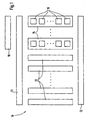
- Figure 1 is a schematic block diagram of an electrical system comprising at least one function board and at least one power supply board
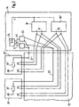
- figure 2 is a more detailed schematic block diagram of the function boards and the power supply board of figure 1
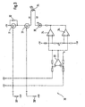
- figure 3 is a schematic diagram of an electrical circuit comprised in the power supply board of figure 2.
- an electrical system 10 for example an electrical testing system for testing the channels of a communication system.
- the electrical system 10 is comprised in a rack or the like which provides a front plane board 11 and a back plane board 12. In between the front plane board 11 and the back plane board 12, a number of boards may be plugged into the rack.
- the electrical system 10 is provided with a number of function boards 13 and a number of power supply boards 14.
- the function boards 13 may e.g. comprise the electrical circuits for testing the channels of the communication system. As an example, eight so-called channel boards may be present within the electrical system 10.
- the power supply boards 14 comprise the electrical circuits for creating the required voltages for the function boards. As an example, four such power supply boards 14 may be present within the electrical system 10.
- Each one of the power supply boards 14 comprises a number of voltage converters 15 wherein each one of these voltage converters 15 is used to create one of the required voltages. As an example, five voltage converters 15 are present within each one of the power supply boards 14.
- the front plane board 11 and the back plane board 12 comprise the connections between the function boards 13 and the power supply boards 14.
- the front plane board 11 and the back plane board 12 provide grounds for the electrical circuits on the function boards 13 and the power supply boards 14, i.e. a front plane ground and a back plane ground.
- a power control board 16 is connected to the front plane board 11 which comprises electrical circuits in particular for controlling the voltages created on the power supply boards 14.
- the voltage converter 15' creates a first voltage U1 and the voltage converter 15" creates a second voltage U2.
- the two voltages U1, U2 may be different or equal.
- the electrical system 10 of figure 1 comprises features as described below in connection with figure 2. It is mentioned that ⁇ although the two function boards 13', 13" are shown in figure 2 - only one of them or even none of the two function boards 13', 13" may actually be present. This - unknown - state of the electrical system 10 is detected as described below.
- the function board 13' is provided with a first resistor 20' and the function board 13" is provided with a second resistor 20".
- Each one of the two resistors 20', 20" is supplied with a voltage UR, e.g. - 12 V which may be taken e.g. from the back plane board 12.
- the resistors 20', 20" identify the corresponding function board 13', 13". This means that a specific function board is provided with a specific value of its resistor wherein the specific value of the resistor unambiguously identifies the function board. If, therefore, the values of the two resistors 20', 20" of the two function boards 13', 13" are different, then the two function boards 13', 13" are different. If, however, the values of the two resistors 20', 20" of the two function boards 13', 13" are identical, then the two function boards 13', 13" are identical.
- each one of the two resistors 20', 20" is connected to the power supply board 14 via the back plane board 12.
- the respective connections are characterized by the reference numerals 21', 21 ".
- the two connections 21', 21" are connected to a first evaluation circuit 22 and to a second evaluation circuit 23, respectively.
- the two evaluation circuits 22, 23 are coupled via an optical coupler 24 as described later.
- the first evaluation circuit 22 checks whether two resistors 20', 20" are present.
- the output signal O1 of the first evaluation circuit 22 is "conductive” if two resistors 20', 20" and therefore the two function boards 13', 13" are present.
- the output signal O1 of the first evaluation circuit 22 is "non-conductive” if only one or no resistor 20', 20" and therefore only one or none of the two function boards 13', 13" is present.
- the second evaluation circuit 23 checks whether the two resistors 20', 20" are identical.
- the output signal O2 of the second evaluation circuit 23 is "high” if the two resistors 20', 20" and therefore the two function boards 13', 13" are identical.
- the output signal O2 of the second evaluation circuit 23 is "low” if the resistors 20', 20" and therefore the two function boards 13', 13" are not identical.
- the evaluation circuit 22 may be carried out e.g. with the help of two transistors 31 whose gates are connected to the resistors 20', 20", if present.
- the two transistors 31 are connected in series to a supply voltage wherein that transistor 31 which is not connected directly to the supply voltage, is coupled via a resistor 32 to the supply voltage.
- Each one of the two transistors 31 is in its non-conducting state if the corresponding resistor 20', 20" is not present. As a result, the output signal O1 of the two transistors is "non-conductive". If only one of the two resistors 20', 20" is present, only one of the two transistors 31 is switched to its conducting state. However, due to the serial connection of the two transistors 31, the output signal O1 remains “non-conductive”. Only if both resistors 20', 20" are present, then both transistors 31 are in their conducting state so that the output signal O1 becomes "conductive".
- the evaluation circuit 23 may be carried out e.g. with the help of an operational amplifier 33 whose positive and negative inputs are connected to the two resistors 20', 20" respectively.
- the output of the operational amplifier 33 is connected to a comparator comprising two operational amplifiers 34.
- These operational amplifiers 34 are connected to a number of resistors so that an upper and a lower threshold value is defined by the two operational amplifiers 34 such that a zero voltage is in between these two threshold values.
- the output of the operational amplifier 33 is about a zero voltage. This zero voltage is detected by the two operational amplifiers 34 to be in between the two threshold values. Therefore, none of the two operational amplifiers 34 of the comparator creates an output voltage which corresponds to the output signal O2 to be "high". However, if the two resistors 20', 20" are different, the output of the operational amplifier 33 corresponds to a voltage which is outside of the two threshold values of the comparator which are defined by the two operational amplifiers 34. This has the result that one of the operational amplifiers 34 creates a negative output voltage which corresponds to the output signal O2 to be "low".
- the optical coupler 24 is connected in between the signals O1 and O2. Furthermore, a light emitting diode (LED) 35 is provided in this path. If the signal O1 is "conductive", a current could flow from the power supply to the optical coupler 24. However, this current can only flow if the signal O2 is "low”. If this is the case, the current flows from the power supply to the LED 35 so that the LED 35 produces e.g. a red alarm light.
- LED light emitting diode
- the LED 35 is turned on if two function boards 13', 13" are present (signal O1 is “conductive”) and if the two function boards 13', 13" are not identical (signal O2 is "low”). Therefore, the LED 35 produces an alarm if the requirement of two identical function boards 13', 13" is not fulfilled.
- the signal O1 is "non-conductive" so that no current can flow to the optical coupler 24 or the LED 35. Again, the LED 35 does not show an alarm.
- the output of the optical coupler 24 is connected to each one of the two voltage converters 15', 15".
- the above described electrical system 10 may also comprise only a single voltage converter so that only a single voltage is provided to the two function boards.
- the alarm signal A of the optical coupler 24 is only connected to this single voltage converter.
Landscapes
- Engineering & Computer Science (AREA)
- General Engineering & Computer Science (AREA)
- Physics & Mathematics (AREA)
- General Physics & Mathematics (AREA)
- Tests Of Electronic Circuits (AREA)
- Testing Electric Properties And Detecting Electric Faults (AREA)
- Testing Of Short-Circuits, Discontinuities, Leakage, Or Incorrect Line Connections (AREA)
Description
- The invention relates to an electrical system like a testing system for testing the channels of a communication system.
- Such electrical system comprises two function boards and at least one voltage converter, wherein the function boards and the voltage converter are connected such that a voltage provided by the voltage converter is supplied to the function boards. In an electrical testing system, the function boards may be realized by so-called channel boards wherein none or one or two function boards may be plugged in and may therefore be present in the electrical system.
- In such an electrical system, it is often required that, if two function boards are present, these two function boards are identical. If this requirement is not fulfilled, the function boards must not be supplied with a voltage.
- EP 0 212 045 A2 relates to an electrical system for automatically adapting the measurement range of a display instrument or a computing instrument to the range of output voltages of a sensor for a physical entity said sensor being voltage-supplied by the display instrument. For that purpose, the sensor comprises an identification resistor and the instrument comprises an identification circuit.
- It is an object of the invention to provide an electrical system as described above with the ability to check whether two function boards are present and whether these two function boards are identical.
- This object is solved by an electrical system according to claim 1.
- In particular, the electrical system comprises an electrical circuit for checking whether two function boards are present and whether these two function boards are identical, and for disabling the voltage converter under the condition that two non-identical function boards are present.
- The invention therefore provides an electrical system which automatically detects its own state. Under the condition that two function boards are present and that these two function boards are not identical, the electrical system ensures that the two function boards are not supplied with a voltage. In all other cases, i.e. if two identical function boards are present or if only one function board is present, the function board/s are/is supplied with a voltage.
- The invention automatically avoids the risk that a supply voltage is forwarded to one of the function boards if the above requirement is not met. Thereby, it is ensured that the function boards are not damaged due to non-allowed conditions, in particular non-allowed voltages.
- In an advantageous embodiment of the invention, the electrical system comprises a resistor on each one of the function boards wherein a specific value of the resistor unambiguously defines the corresponding function board. The invention, therefore, provides a resistor which is dedicated to each function board and which defines the function board. In particular, different resistors define different function boards. As a result, it is possible to detect the identity of the two function boards by comparing'the values of the resistors of these two function boards.
- The invention together with further objects, advantages, features and aspects thereof will be more clearly understood from the following description taken in connection with the accompanying drawings.
- Figure 1 is a schematic block diagram of an electrical system comprising at least one function board and at least one power supply board, figure 2 is a more detailed schematic block diagram of the function boards and the power supply board of figure 1, and figure 3 is a schematic diagram of an electrical circuit comprised in the power supply board of figure 2.
- In figure 1, an
electrical system 10 is shown, for example an electrical testing system for testing the channels of a communication system. Theelectrical system 10 is comprised in a rack or the like which provides afront plane board 11 and aback plane board 12. In between thefront plane board 11 and theback plane board 12, a number of boards may be plugged into the rack. - As shown in figure 1, the
electrical system 10 is provided with a number offunction boards 13 and a number ofpower supply boards 14. Thefunction boards 13 may e.g. comprise the electrical circuits for testing the channels of the communication system. As an example, eight so-called channel boards may be present within theelectrical system 10. Thepower supply boards 14 comprise the electrical circuits for creating the required voltages for the function boards. As an example, four suchpower supply boards 14 may be present within theelectrical system 10. - Each one of the
power supply boards 14 comprises a number ofvoltage converters 15 wherein each one of thesevoltage converters 15 is used to create one of the required voltages. As an example, fivevoltage converters 15 are present within each one of thepower supply boards 14. - The
front plane board 11 and theback plane board 12 comprise the connections between thefunction boards 13 and thepower supply boards 14. - As well, the
front plane board 11 and theback plane board 12 provide grounds for the electrical circuits on thefunction boards 13 and thepower supply boards 14, i.e. a front plane ground and a back plane ground. - Furthermore, a
power control board 16 is connected to thefront plane board 11 which comprises electrical circuits in particular for controlling the voltages created on thepower supply boards 14. - In figure 2, two
function boards 13', 13", theback plane board 12 and one of thepower supply boards 14 with twovoltage converters 15', 15" are shown. - The voltage converter 15' creates a first voltage U1 and the
voltage converter 15" creates a second voltage U2. The two voltages U1, U2 may be different or equal. - These two voltages U1, U2 are provided to each one of the two
function boards 13', 13". The electrical connections between thevoltage converters 15', 15" and thefunction boards 13', 13" are carried out via theback plane board 12. - In particular in an electrical testing system, it is often required that two channel boards are identical. If at least two channel boards are present, this requirement must be fulfilled. Otherwise, the channel boards must not be supplied with a voltage. If only one channel board is present, this requirement is not relevant and must not be fulfilled.
- In order to check this requirement, the
electrical system 10 of figure 1 comprises features as described below in connection with figure 2. It is mentioned that ― although the twofunction boards 13', 13" are shown in figure 2 - only one of them or even none of the twofunction boards 13', 13" may actually be present. This - unknown - state of theelectrical system 10 is detected as described below. - As shown in figure 2, the function board 13' is provided with a first resistor 20' and the
function board 13" is provided with asecond resistor 20". Each one of the tworesistors 20', 20" is supplied with a voltage UR, e.g. - 12 V which may be taken e.g. from theback plane board 12. - The
resistors 20', 20" identify thecorresponding function board 13', 13". This means that a specific function board is provided with a specific value of its resistor wherein the specific value of the resistor unambiguously identifies the function board. If, therefore, the values of the tworesistors 20', 20" of the twofunction boards 13', 13" are different, then the twofunction boards 13', 13" are different. If, however, the values of the tworesistors 20', 20" of the twofunction boards 13', 13" are identical, then the twofunction boards 13', 13" are identical. - As shown in figure 2, each one of the two
resistors 20', 20" is connected to thepower supply board 14 via theback plane board 12. The respective connections are characterized by thereference numerals 21', 21 ". - On the
power supply board 14, the twoconnections 21', 21" are connected to afirst evaluation circuit 22 and to asecond evaluation circuit 23, respectively. The twoevaluation circuits optical coupler 24 as described later. - The
first evaluation circuit 22 checks whether tworesistors 20', 20" are present. The output signal O1 of thefirst evaluation circuit 22 is "conductive" if tworesistors 20', 20" and therefore the twofunction boards 13', 13" are present. However, the output signal O1 of thefirst evaluation circuit 22 is "non-conductive" if only one or noresistor 20', 20" and therefore only one or none of the twofunction boards 13', 13" is present. - The
second evaluation circuit 23 checks whether the tworesistors 20', 20" are identical. The output signal O2 of thesecond evaluation circuit 23 is "high" if the tworesistors 20', 20" and therefore the twofunction boards 13', 13" are identical. However, the output signal O2 of thesecond evaluation circuit 23 is "low" if theresistors 20', 20" and therefore the twofunction boards 13', 13" are not identical. - In figure 3, an
electrical circuit 30 is shown which realizes the first and thesecond evaluation circuits - The
evaluation circuit 22 may be carried out e.g. with the help of twotransistors 31 whose gates are connected to theresistors 20', 20", if present. The twotransistors 31 are connected in series to a supply voltage wherein thattransistor 31 which is not connected directly to the supply voltage, is coupled via aresistor 32 to the supply voltage. - Each one of the two
transistors 31 is in its non-conducting state if the correspondingresistor 20', 20" is not present. As a result, the output signal O1 of the two transistors is "non-conductive". If only one of the tworesistors 20', 20" is present, only one of the twotransistors 31 is switched to its conducting state. However, due to the serial connection of the twotransistors 31, the output signal O1 remains "non-conductive". Only if bothresistors 20', 20" are present, then bothtransistors 31 are in their conducting state so that the output signal O1 becomes "conductive". - The
evaluation circuit 23 may be carried out e.g. with the help of an operational amplifier 33 whose positive and negative inputs are connected to the tworesistors 20', 20" respectively. The output of the operational amplifier 33 is connected to a comparator comprising twooperational amplifiers 34. Theseoperational amplifiers 34 are connected to a number of resistors so that an upper and a lower threshold value is defined by the twooperational amplifiers 34 such that a zero voltage is in between these two threshold values. - If both
resistors 20', 20" have the identical value, the output of the operational amplifier 33 is about a zero voltage. This zero voltage is detected by the twooperational amplifiers 34 to be in between the two threshold values. Therefore, none of the twooperational amplifiers 34 of the comparator creates an output voltage which corresponds to the output signal O2 to be "high". However, if the tworesistors 20', 20" are different, the output of the operational amplifier 33 corresponds to a voltage which is outside of the two threshold values of the comparator which are defined by the twooperational amplifiers 34. This has the result that one of theoperational amplifiers 34 creates a negative output voltage which corresponds to the output signal O2 to be "low". - According to figure 3, the
optical coupler 24 is connected in between the signals O1 and O2. Furthermore, a light emitting diode (LED) 35 is provided in this path. If the signal O1 is "conductive", a current could flow from the power supply to theoptical coupler 24. However, this current can only flow if the signal O2 is "low". If this is the case, the current flows from the power supply to theLED 35 so that theLED 35 produces e.g. a red alarm light. - As a result, the
LED 35 is turned on if twofunction boards 13', 13" are present (signal O1 is "conductive") and if the twofunction boards 13', 13" are not identical (signal O2 is "low"). Therefore, theLED 35 produces an alarm if the requirement of twoidentical function boards 13', 13" is not fulfilled. - If, however, two
identical function boards 13', 13" are present, then the signal O2 is "high". The described current can therefore not flow via theoptical coupler 24 and theLED 35. TheLED 35 therefore does not show an alarm. - The same is valid if only one
function board 13', 13" is present. In this case, the signal O1 is "non-conductive" so that no current can flow to theoptical coupler 24 or theLED 35. Again, theLED 35 does not show an alarm. - As shown in figure 2, the output of the
optical coupler 24 is connected to each one of the twovoltage converters 15', 15". - As described, if two
non-identical function boards 13', 13" are present, a current flows via theoptical coupler 24 and theLED 35. In this case, theoptical coupler 24 therefore creates an alarm signal A. This alarm signal A is provided to the twovoltage converters 15', 15" so that these twovoltage converters 15', 15" are disabled, i.e. turned off. - In all other cases, i.e. if two
identical function boards 13', 13" are present or if only onefunction board 13', 13" is present, then no current flows via theoptical coupler 24. Therefore, no alarm signal A is forwarded to the twovoltage converters 15', 15". This results in the creation of the two voltages U1, U2 and the provision of these two voltages U1, U2 to thefunction boards 13', 13". - It shall be mentioned that the above described
electrical system 10 may also comprise only a single voltage converter so that only a single voltage is provided to the two function boards. In this case, the alarm signal A of theoptical coupler 24 is only connected to this single voltage converter.
Claims (8)
- An electrical system (10) comprising none or one or two function boards (13', 13") and at least one voltage converter (15'), wherein the plugged-in function board/s (13', 13") and the voltage converter (15') are connected such that a voltage (U1) provided by the voltage converter (15') is supplied to the plugged-in function board/s (13', 13"), and comprising an electrical circuit (22, 23; 30) for checking whether two function boards (13', 13") are present and whether these two function boards (13', 13") are identical, and for disabling the voltage converter (15') under the condition that two non-identical function boards (13', 13") are present.
- The electrical system (10) of claim 1 comprising a resistor (20', 20") on each one of the function boards (13', 13") wherein different values of the resistor (20', 20") define different function boards (13', 13") .
- The electrical system (10) of claim 1 comprising an evaluation circuit (22) for checking whether two function boards (13', 13") are present and for creating a first output signal (O1).
- The electrical system (10) of claim 2 comprising two serially connected transistors (31) wherein the base of one of the two transistors (31) is connected to one of the two resistors (20', 20") of the two function boards (13', 13") and the base of the other one of the two transistors (31) is connected to the other one of the two resistors (20', 20").
- The electrical system (10) of claim 1 comprising an evaluating circuit (23) for checking whether the two function boards (13', 13") are identical and for creating a second output signal (O2).
- The electrical system (10) of claim 2 comprising a first operational amplifier (33) wherein an input of the first operational amplifier (33) is connected to one of the two resistors (20', 20") of the two function boards (13', 13") and the other input of the first operational amplifier (33) is connected to the other one of the two resistors (20', 20"), and comprising two further operational amplifiers (34) being connected to the output of the first operational amplifier (33) and establishing an upper and a lower threshold value.
- The electrical system (10) having the features of claims 3 and 5 comprising an alarm circuit, in particular an optical coupler (24) for enabling or disabling the voltage converter (15') depending on the two output signals (O1, O2).
- The electrical system (10) of claim 1 wherein the function boards (13', 13") are so-called channel boards for testing the channels of a communication system.
Priority Applications (4)
| Application Number | Priority Date | Filing Date | Title |
|---|---|---|---|
| DE60200213T DE60200213T2 (en) | 2002-04-06 | 2002-04-06 | Electrical system for checking the channels in a communication system |
| EP02007780A EP1271167B1 (en) | 2002-04-06 | 2002-04-06 | Electrical System for testing the channels of a communication system |
| US10/304,513 US7149286B2 (en) | 2002-04-06 | 2002-11-26 | Electrical system like a system for testing the channels of a communication system |
| JP2003099337A JP2003315399A (en) | 2002-04-06 | 2003-04-02 | Electrical test system for testing channels of communication system |
Applications Claiming Priority (1)
| Application Number | Priority Date | Filing Date | Title |
|---|---|---|---|
| EP02007780A EP1271167B1 (en) | 2002-04-06 | 2002-04-06 | Electrical System for testing the channels of a communication system |
Publications (2)
| Publication Number | Publication Date |
|---|---|
| EP1271167A1 EP1271167A1 (en) | 2003-01-02 |
| EP1271167B1 true EP1271167B1 (en) | 2004-02-18 |
Family
ID=8185447
Family Applications (1)
| Application Number | Title | Priority Date | Filing Date |
|---|---|---|---|
| EP02007780A Expired - Lifetime EP1271167B1 (en) | 2002-04-06 | 2002-04-06 | Electrical System for testing the channels of a communication system |
Country Status (4)
| Country | Link |
|---|---|
| US (1) | US7149286B2 (en) |
| EP (1) | EP1271167B1 (en) |
| JP (1) | JP2003315399A (en) |
| DE (1) | DE60200213T2 (en) |
Families Citing this family (2)
| Publication number | Priority date | Publication date | Assignee | Title |
|---|---|---|---|---|
| TWI274166B (en) * | 2004-06-18 | 2007-02-21 | Unitest Inc | Semiconductor test apparatus for simultaneously testing plurality of semiconductor devices |
| US7707286B2 (en) * | 2006-05-11 | 2010-04-27 | Sonim Technologies, Inc. | Methods for managing presence information in a real-time communications network |
Citations (1)
| Publication number | Priority date | Publication date | Assignee | Title |
|---|---|---|---|---|
| EP0212045A2 (en) * | 1985-07-11 | 1987-03-04 | Raimund Wilhelm | Adaptation of a display or evaluation device to a sensor |
Family Cites Families (8)
| Publication number | Priority date | Publication date | Assignee | Title |
|---|---|---|---|---|
| US3890559A (en) * | 1974-05-20 | 1975-06-17 | Gte Automatic Electric Lab Inc | Circuit for monitoring and controlling multiple power supplies |
| US4541094A (en) * | 1983-03-21 | 1985-09-10 | Sequoia Systems, Inc. | Self-checking computer circuitry |
| US4947427A (en) * | 1987-05-15 | 1990-08-07 | Northern Telecom Limited | Protection arrangement for a telephone subscriber line interface circuit |
| US6247144B1 (en) * | 1991-01-31 | 2001-06-12 | Compaq Computer Corporation | Method and apparatus for comparing real time operation of object code compatible processors |
| JPH05251519A (en) * | 1992-01-09 | 1993-09-28 | Nec Corp | Tester for measuring semiconductor device |
| US5909591A (en) * | 1996-06-18 | 1999-06-01 | Lucent Technologies Inc. | System and method for identifying individual modules in a modular system |
| JPH11155233A (en) * | 1997-11-25 | 1999-06-08 | Advantest Corp | Dc power supply equipment |
| US6459275B1 (en) * | 2001-02-28 | 2002-10-01 | Avaya Technology Corp. | Detection of devices on a local area network |
-
2002
- 2002-04-06 DE DE60200213T patent/DE60200213T2/en not_active Expired - Fee Related
- 2002-04-06 EP EP02007780A patent/EP1271167B1/en not_active Expired - Lifetime
- 2002-11-26 US US10/304,513 patent/US7149286B2/en not_active Expired - Fee Related
-
2003
- 2003-04-02 JP JP2003099337A patent/JP2003315399A/en active Pending
Patent Citations (1)
| Publication number | Priority date | Publication date | Assignee | Title |
|---|---|---|---|---|
| EP0212045A2 (en) * | 1985-07-11 | 1987-03-04 | Raimund Wilhelm | Adaptation of a display or evaluation device to a sensor |
Also Published As
| Publication number | Publication date |
|---|---|
| JP2003315399A (en) | 2003-11-06 |
| US20030189430A1 (en) | 2003-10-09 |
| DE60200213T2 (en) | 2004-12-16 |
| EP1271167A1 (en) | 2003-01-02 |
| DE60200213D1 (en) | 2004-03-25 |
| US7149286B2 (en) | 2006-12-12 |
Similar Documents
| Publication | Publication Date | Title |
|---|---|---|
| KR101517353B1 (en) | Led outage detection circuit | |
| CN100549973C (en) | A kind of usb bus interface detection apparatus and detection method thereof | |
| US20120153993A1 (en) | Usb port detecting circuit | |
| US8290748B2 (en) | Sensor interface with integrated current measurement | |
| US4149160A (en) | Multi-input signal comparator and indicator circuit | |
| EP1271167B1 (en) | Electrical System for testing the channels of a communication system | |
| WO2014148706A1 (en) | Apparatus for discriminating type of analog sensor | |
| US20120319663A1 (en) | Load-testing circuit for usb ports | |
| US20090014631A1 (en) | Signal detection circuit and signal detection method, and state detection circuit | |
| CN207782765U (en) | Key detection circuit integrated with ambient brightness detection | |
| US10326360B2 (en) | Power supplying device | |
| KR970049834A (en) | Presence detection system for integrated circuits on electrically conductive objects, especially on chip cards | |
| EP2362711B1 (en) | Failure detection of LEDs | |
| CN114347790B (en) | High-voltage interlocking detection circuit and electronic equipment | |
| CN214427480U (en) | Multi-path voltage detection circuit and test fixture | |
| IE51941B1 (en) | A variable impedance circuit | |
| EP1365252B1 (en) | Current direction detection | |
| EP1271168B1 (en) | Electrical system for testing the channels of a communication system | |
| US20100127688A1 (en) | Current load driving device | |
| CN216013572U (en) | Assembly line test multi-output power management control panel | |
| CN219609185U (en) | LED driving current detection circuit, LED detection device and stage lamp thereof | |
| CN219041460U (en) | Power supply circuit, power supply circuit board and power supply equipment | |
| KR20060130286A (en) | A structure for reduction of input signal port in a control unit of vehicle | |
| KR20230006676A (en) | System for IGBT module test of railway vehicle | |
| KR100298901B1 (en) | Load share control apparatus of non isolation dc/dc converter using current mirror |
Legal Events
| Date | Code | Title | Description |
|---|---|---|---|
| PUAI | Public reference made under article 153(3) epc to a published international application that has entered the european phase |
Free format text: ORIGINAL CODE: 0009012 |
|
| 17P | Request for examination filed |
Effective date: 20021024 |
|
| AK | Designated contracting states |
Kind code of ref document: A1 Designated state(s): AT BE CH CY DE DK ES FI FR GB GR IE IT LI LU MC NL PT SE TR |
|
| AX | Request for extension of the european patent |
Free format text: AL;LT;LV;MK;RO;SI |
|
| 17Q | First examination report despatched |
Effective date: 20030221 |
|
| GRAP | Despatch of communication of intention to grant a patent |
Free format text: ORIGINAL CODE: EPIDOSNIGR1 |
|
| AKX | Designation fees paid |
Designated state(s): DE FR GB |
|
| GRAS | Grant fee paid |
Free format text: ORIGINAL CODE: EPIDOSNIGR3 |
|
| GRAA | (expected) grant |
Free format text: ORIGINAL CODE: 0009210 |
|
| AK | Designated contracting states |
Kind code of ref document: B1 Designated state(s): DE FR GB |
|
| PG25 | Lapsed in a contracting state [announced via postgrant information from national office to epo] |
Ref country code: FR Free format text: LAPSE BECAUSE OF FAILURE TO SUBMIT A TRANSLATION OF THE DESCRIPTION OR TO PAY THE FEE WITHIN THE PRESCRIBED TIME-LIMIT Effective date: 20040218 |
|
| REG | Reference to a national code |
Ref country code: GB Ref legal event code: FG4D |
|
| REG | Reference to a national code |
Ref country code: IE Ref legal event code: FG4D |
|
| REF | Corresponds to: |
Ref document number: 60200213 Country of ref document: DE Date of ref document: 20040325 Kind code of ref document: P |
|
| PLBE | No opposition filed within time limit |
Free format text: ORIGINAL CODE: 0009261 |
|
| STAA | Information on the status of an ep patent application or granted ep patent |
Free format text: STATUS: NO OPPOSITION FILED WITHIN TIME LIMIT |
|
| REG | Reference to a national code |
Ref country code: IE Ref legal event code: MM4A |
|
| EN | Fr: translation not filed | ||
| 26N | No opposition filed |
Effective date: 20041119 |
|
| PGFP | Annual fee paid to national office [announced via postgrant information from national office to epo] |
Ref country code: GB Payment date: 20070411 Year of fee payment: 6 |
|
| PGFP | Annual fee paid to national office [announced via postgrant information from national office to epo] |
Ref country code: DE Payment date: 20080411 Year of fee payment: 7 |
|
| GBPC | Gb: european patent ceased through non-payment of renewal fee |
Effective date: 20080406 |
|
| PG25 | Lapsed in a contracting state [announced via postgrant information from national office to epo] |
Ref country code: GB Free format text: LAPSE BECAUSE OF NON-PAYMENT OF DUE FEES Effective date: 20080406 |
|
| PG25 | Lapsed in a contracting state [announced via postgrant information from national office to epo] |
Ref country code: DE Free format text: LAPSE BECAUSE OF NON-PAYMENT OF DUE FEES Effective date: 20091103 |