EP0204584A2 - Vorrichtung und Verfahren für die Erfassung der Polarisation des Elektronenspins - Google Patents
Vorrichtung und Verfahren für die Erfassung der Polarisation des Elektronenspins Download PDFInfo
- Publication number
- EP0204584A2 EP0204584A2 EP86304346A EP86304346A EP0204584A2 EP 0204584 A2 EP0204584 A2 EP 0204584A2 EP 86304346 A EP86304346 A EP 86304346A EP 86304346 A EP86304346 A EP 86304346A EP 0204584 A2 EP0204584 A2 EP 0204584A2
- Authority
- EP
- European Patent Office
- Prior art keywords
- target
- electrons
- electron
- scattering
- energy
- Prior art date
- Legal status (The legal status is an assumption and is not a legal conclusion. Google has not performed a legal analysis and makes no representation as to the accuracy of the status listed.)
- Granted
Links
Images


Classifications
-
- G—PHYSICS
- G21—NUCLEAR PHYSICS; NUCLEAR ENGINEERING
- G21K—TECHNIQUES FOR HANDLING PARTICLES OR IONISING RADIATION NOT OTHERWISE PROVIDED FOR; IRRADIATION DEVICES; GAMMA RAY OR X-RAY MICROSCOPES
- G21K1/00—Arrangements for handling particles or ionising radiation, e.g. focusing or moderating
- G21K1/16—Arrangements for handling particles or ionising radiation, e.g. focusing or moderating using polarising devices, e.g. for obtaining a polarised beam
-
- G—PHYSICS
- G01—MEASURING; TESTING
- G01T—MEASUREMENT OF NUCLEAR OR X-RADIATION
- G01T1/00—Measuring X-radiation, gamma radiation, corpuscular radiation, or cosmic radiation
- G01T1/32—Measuring polarisation of particles
-
- G—PHYSICS
- G11—INFORMATION STORAGE
- G11B—INFORMATION STORAGE BASED ON RELATIVE MOVEMENT BETWEEN RECORD CARRIER AND TRANSDUCER
- G11B11/00—Recording on or reproducing from the same record carrier wherein for these two operations the methods are covered by different main groups of groups G11B3/00 - G11B7/00 or by different subgroups of group G11B9/00; Record carriers therefor
- G11B11/10—Recording on or reproducing from the same record carrier wherein for these two operations the methods are covered by different main groups of groups G11B3/00 - G11B7/00 or by different subgroups of group G11B9/00; Record carriers therefor using recording by magnetic means or other means for magnetisation or demagnetisation of a record carrier, e.g. light induced spin magnetisation; Demagnetisation by thermal or stress means in the presence or not of an orienting magnetic field
- G11B11/115—Recording on or reproducing from the same record carrier wherein for these two operations the methods are covered by different main groups of groups G11B3/00 - G11B7/00 or by different subgroups of group G11B9/00; Record carriers therefor using recording by magnetic means or other means for magnetisation or demagnetisation of a record carrier, e.g. light induced spin magnetisation; Demagnetisation by thermal or stress means in the presence or not of an orienting magnetic field using a beam,e.g. of electrons or X-rays other than a beam of light for reproducing
Definitions
- This invention relates to electron spin polarization and more particularly, to the measurement of electron spin polarization via low energy diffuse scattering.
- An electron in addition to being characterized by its energy and momentum, is characterized by a quantity known as its spin.
- a beam of electrons necessarily contains a large number of electrons where each individual electron contributes a spin, either up or down. If a greater population of one electron spin type exists in the beam, then the beam is spin polarized.
- the spin polarization of the beam is quantifiable by the following equation: where N electrons have their spins in the up up direction and Ndn spins are pointing down. P represents the net orientation of the beam or ensemble of electrons. P values may range from +1 (all spins up), to 0 (an equal number of spins up and down), to -1 (all spins down).
- the preselected "up/down" polarization axis is arbitrary as to where it is oriented relative to the coordinate system used for measurement. It is preferred, for purposes of interpretation, to employ a cartesian coordinate scheme where the determination of the cartesian components of the polarization of the electron beam, P ,P , and P , is equivalent to the x y z determination of the magnitude and direction of the polarization vector.
- a beam with vector polarization is further characterized as transversely polarized when the polarization is perpendicular to its velocity and longitudinally polarized, when the vector polarization is parallel to its velocity direction.
- Known sources for producing beams of polarized electrons include photoemission from GaAs, described in United States Patent 3,968,376; and secondary emission from a ferromagnet, as discussed by Unguris et al in The Physical Review Letters 47,72(1982). Because an electron has a spin of h/(4pi) and this spin has an associated magnetic moment of one Bohr magneton, a measurement of the electron spin orientation yields information about, for example, the origin of the electron or its interactions.
- An example of the uses of electron spin polarization for analytical applications includes the 10 scattering of very high energy electrons (10 eV) from other elementary particles to test the violation of the physical law of parity conservation.
- Another use involves measurement of the interaction characteristics of an electron with an isolated atom, including measurement of the polarization of the electron before and after scattering. Such measurement demonstrates the extent of electron substitution within the atom and/or the degree of electron deflection from the atomic charge cloud. Additionally, spin polarization measurements may be used for probing solid materials in the case of ferromagnetic materials due to the fact that electrons emitted from a ferromagnetic material either by photoemission, field emission, or secondary emission can be used to characterize the magnetic nature of the material.
- Information storage mechanisms now exist in which magnetic domains in ferromagnetic materials are oriented parallel or antiparallel relative to particular reference coordinates.
- the development of high density, magnetic storage mechanisms is contingent upon the microscopic investigation of magnetic domains which is enhanced by the use of electron polarization detection.
- Information so stored can be "read” by measuring the spin polarization of electrons emitted therefrom.
- a finely focused electron beam e.g. a scanning electron microscope
- the spin polarization of the emitted electrons can be measured.
- Mott scattering The traditional means of measuring electron spin polarization is known as Mott scattering, after S ir Neville Mott.
- the Mott detector measures the backscattered intensity for equal angles to the right and left of the beam's incident direction to determine the degree of polarization normal to the scattering plane.
- the normal component to the scattering plane is defined as where A is the scattering asymmetry; I R and I L are respectively, the scattered electron intensities to the right side of the beam and the left, and S is the analyzing power which depends on the scattering target and the particular scattering geometry.
- the Mott detector employing a thin gold foil target in the thickness range of 300-1500 Angstroms, is calibrated to determine the effective analyzing power, S, by using theoretical calculations of the spin asymmetry in scattering 100,000 to 120,000 electron volt electrons.
- the Mott detector employs very thin gold foils for the target.
- the calibration of the detector involves a series of measurements of polarized electron beam scattering for well-defined geometries as a function of the target foil thickness.
- the Mott device suffers reduced efficiency as a result of many of the incident electrons passing through the scattering target, i.e. the target is not opaque to the electron beam. At 100,000 electron volts, the target is not opaque to the high energy electrons where the mean free path of the electrons is sufficiently long so that characterize the magnetic nature of the material.
- Information storage mechanisms now exist in which magnetic domains in ferromagnetic materials are oriented parallel or antiparallel relative to particular reference coordinates.
- the development of high density, magnetic storage mechanisms is contingent upon the microscopic investigation of magnetic domains which is enhanced by the use of electron polarization detection.
- Information so stored can be "read” by measuring the spin polarization of electrons emitted therefrom.
- a finely focused electron beam e.g. a scanning electron microscope
- the spin polarization of the emitted electrons can be measured.
- Mott scattering The traditional means of measuring electron spin polarization is known as Mott scattering, after Sir Neville Mott.
- the Mott detector measures the backscattered intensity for equal angles to the right and left of the beam's incident direction to determine the degree of polarization normal to the scattering plane.
- the normal component to the scattering plane is defined as where A is the scattering asymmetry; I R and I L are respectively, the scattered electron intensities to the right side of the beam and the left, and S is the analyzing power which depends on the scattering target and the particular scattering geometry.
- the Mott detector employing a thin gold foil target in the thickness range of 300-1500 Angstroms, is calibrated to determine the effective analyzing power, S, by using theoretical calculations of the spin asymmetry in scattering 100,000 to 120,000 electron volt electrons.
- the Mott detector employs very thin gold foils for the target.
- the calibration of the detector involves a series of measurements of polarized electron beam scattering for well-defined geometries as a function of the target foil thickness.
- the Mott device suffers reduced efficiency as a result of many of the incident electrons passing through the scattering target, i.e. the target is not opaque to the electron beam.
- the target is not opaque to the high energy electrons where the mean free path of the electrons is sufficiently long so that many pass through the thin gold foil.
- thin foils typically only about 0.01% of the electrons entering the device are back scattered into the detectors actually used in the measurement.
- low energy electrons with energies less than a few thousand electron volts
- the target opacity depends on both the electron energy and the target density.
- the mercury beam is often corrosive. Also, like the Mott Detector, the mercury atomic beam suffers detection inefficiencies caused by the target not being opaque to the electron beam. These inefficiencies are caused, in the case of the mercury atomic beam, by low target density.
- the Kirschner detector is distinguishable from the above-described devices as it employs an opaque monocrystal scattering target for determining electron spin dependent interactions.
- the spin dependent interaction is the spin orbit interaction in the scattering of the incident electrons from the monocrystal.
- the monocrystal presents an orderly arrangement of atoms in crystal planes which, upon electron beam impingement, causes the electrons to be diffracted backward into well defined beams. These beams of scattered electrons are symmetrically spaced relative to the electron beam incident on the monocrystal surface. Significant multiple scattering occurs which cannot be reliably calculated thereby necessitating experimental calibration.
- FM S I/I
- the Kirschner device it is necessary for the electron optics to reject much of the electron beam before it reaches the target surface so as to satisfy the severe constraints on spread in angle and energy.
- the I at the target is much 0 smaller and the measurement signal is severely decreased.
- the monocrystal device is efficient only for well collimated beams with narrow energy spread.
- the monocrystal device requires the elimination of any inelastically scattered electrons, (usually those which have lost over 10 electron volts of energy in the scattering process) which results in a loss in useful scattering intensity.
- An object of this invention is to provide an efficient means and method to measure electron spin polarization that is of compact and elegant construction.
- Still another object of this invention is to provide a means of electron spin polarization measurement as efficient or more efficient than the prior art.
- a device for determining the spin polarization of a beam of electrons comprising, beam energy control means for controlling the kinetic energy of the electron beam to less than 10,000 electron volts, target means for impingment of said electron beam, said target means being opaque to said electrons and causing said electrons to diffusely scatter therefrom, collecting means for collecting said electrons scattered within a selected solid angle from said target means, and means for measuring the number of electrons collected from said collecting means.
- a method for determining the spin polarization of an beam composed of electrons comprising the steps of; controlling an electron beam to have an energy of less than 10,000 electron volts, passing the beam to an opaque target, diffusely scattering the electrons from the atoms comprising the target, collecting the diffusely scattered electrons in a selected solid angle, and measuring the number of electrons collected.
- the target surface is easily prepared from polycrystalline or amorphous metals such as gold, mercury, platinum, lead, bismuth, uranium or a semiconductor such as mercury telluride.
- the film may be deposited on an appropriate substrate by sputtering or evaporation.
- the surface of a piece of polycrystalline or amorphous material can be cleaned by conventional means to provide the target surface.
- the scattering surface is an evaporated gold film. Gold being a noble metal is desirable as a stable target due to its especially nonreactive characteristics.
- a scattering target composed of a polycrystalline film, provides sizeable spin dependent asymmetry in the scattering, and this analyzing power is useful over a broad range of incident beam energies.
- the combination of the enhanced energy range and relaxed constraints on the angular divergence of the incident beam gives the present invention a great advantage over the monocrystal spin analyzer as it provides an acceptable detector for a broader range of electron beams.
- a key feature of this invention is to scatter electrons diffusely at low energies from the polycrystalline or amorphous metal or semiconductor target surface and collect those electrons as well as inelastically scattered electrons.
- a target surface is of sufficient density so as to be substantially opaque to the incident electron beam -- electrons do not pass through it.
- scattering from the target surface is diffuse. As a result, scattering is generated from individual atoms, rather than from the crystal planes as in the diffraction from a monocrystal.
- the electron scattering depends not on the orientation of the surface but on the scattering angle, the constraints on the angular divergence of the incident electron beam and on the alignment of the sample surface are minimized.
- the relative weakness of the scattered intensity at a particular scattering angle is compensated by collection of the scattered electrons over a large solid angle.
- the present invention further contemplates that the electron scattering shall take place for electron kinetic energy on the order of 10 -10 electron volts.
- the spin analyzer can be constructed into a very compact unit (fist-sized or less). In view of its relatively diminutive size, it is small enough to be attachable and movable. For example, it may be employed as an energy analyzer inside the vacuum chamber of an angle resolved photoemission apparatus or in other applications the spin analyzer can be enclosed in its own small vacuum chamber.
- the instant invention also detects inelastically scattered electrons which still contribute significantly to the spin dependent asymmetry and can be used to enhance the signal.
- all scattered electrons which have at least 40 electron volts of kinetic energy in the direction normal to the collector can be used leading to a significant increase in efficiency.
- a figure of merit -4 of 10 is readily achieved by this invention when employing a polycrystalline gold film and electron kinetic energies of 150 + 20 electron volts. The device even operates using a larger energy deviation (+ 75 electron volts) from the mean incident kinetic energy. In this case the figure of merit is reduced only by a factor of two which in certain applications may be justified because an energy selector is no longer necessary.
- Control of the electron beam is readily accomplished by conventional electron optical means such as electrostatic or magnetic lenses and deflection plates which transport, change the energy, and focus the beam whereby the beam achieves the appropriate angular divergence and mean energy.
- electron optical means such as electrostatic or magnetic lenses and deflection plates which transport, change the energy, and focus the beam whereby the beam achieves the appropriate angular divergence and mean energy.
- an electron energy selector assists to limit the energy spread of the electrons about the mean energy.
- an electron multiplier assembly enhances electron signal to the detector.
- Low energy secondary electrons can be prevented from reaching the target by establishing a retarding electric field betwen the target and the collector with appropriate grids.
- An additional electron optical means may be employed to change any longitudinal component of electron spin polarization to a transverse component.
- a further advantage of this invention is that it is fully compatible with ultra-high vacuum but only high vacuum is required.
- the analyzing power S of a polycrystaline gold film scattering target was found to decrease only 8% on exposure to air at a pressure of -7 10- Torr for 3.5 days. This suggests that a similar decrease could be expected only after more than a month -8 of use at typical operating pressures of 10 Torr or less.
- the instant invention may be used in other ways too. For example, it is sometimes advantageous to detect the signal composed of all the electrons incident on the target without making a polarization measurement. This might occur when an adjustment of experimental parameters needs to be made where a signal whose intensity has not been degraded by scattering from the target is required. In this case the target may be biased negatively. Thus, the potentials of the electrodes surrounding the scattering region can be adjusted (o prevent the incident electrons from reaching the target and to guide them to the entrance of the backscattered electron collector. In this way, it is easy to switch from making a spin resolved measurement to a non-spin resolved measurement and still use the same signal acquisition system.
- electrons in free space 10 may be generated by any source such as field emission, photoemission, secondary emission, or an electron scattering process (not illustrated).
- the electrons enter the electron optics 12 where they are transported, accelerated or decelerated, focused and guided by conventional electrostatic and/or magnetic electron lenses and deflection plates designated electron optics 12.
- optics 12 consist of a one inch (interior diameter) copper cylinder with 0.1 inch gaps at the cylinder ends.
- Each of the copper lens elements are electrically insulated from each other by alumina spacers.
- the electron energy selector 14 need not have high energy resolution. Any of a number of conventional types such as a cylindrical or spherical condenser type or a plane or cylindrical mirror type is suitable.
- a suitable energy selector consists of a spherical deflector with a mean radius of 1 0 centimeters and potentials of 1811 and 1244 volts respectively to provide a pass energy of 1500 volts.
- selector 14 When selector 14 is operated at a mean energy of 1500 electron volts with 4 mm slits, electrons 10 which have an energy spread of 30 electron volts full width at half maximum pass through selector 14. Electrons 10 escaping energy selector 14 move to electron optics 16 which changes the kinetic energy of electrons to 150 electron volts. Also electrons 10 are then focused to pass through a copper drift tube 15 to guide the electrons through central holes 17 in collecting anode 18, channel multiplier assembly 20, grids 22 and 24, and onto polycrystalline gold film target 26. The drift tube 15 prevents the electrons from seeing the potential on elements 18, 20, 22, and 24 and is insulated from these elements by a 0.005 inch thick Kapton spacer (Dupont trademark). The drift tube l5 ; limits the cone angle of the electron beam to approximately 18°.
- anode 18 in the described embodiment, it is composed of a 2.5 inch diameter, 0 . 12 5 inch thick pyrex plate and coated by vacuum evaporation with a 300 A chromium film, which in turn was evaporation coated with a 5000 A gold film.
- the intermediate chromium layer is employed to improve the adhesion of the gold to the glass.
- a half-inch diameter hole is provided for insertion of drift tube 15 and six holes are provided on the outer periphery to permit the anode to be attached to channel plate assembly 20 .
- alumina spacers separate anode 18 from assembly 20 by approximately 0.15 inches.
- Channel plate assembly 20 has a circular chevron configuration with a 2.5 inch outer diameter and a 0 . 25 inch central bore.
- One such assembly is the Model 3040 available from Galileo Electro-Optics Corp. of Sturbridge, Mass.
- anode 18 and assembly 20 are biased by a resistor divider which provides anode 18 with a voltage of 0.9 V , the back of the channel plate with a voltage o of 0.8 V and the front of the channel plate with a o voltage of 0.15 V where V ranges from 1500 to 3 0 00 o 0 volts with respect to the target 26.
- Grids 22 and 24 approximately 2 inches in diameter, are constructed from 100 line/inch, 0.001 inch diameter stainless steel wire mesh mounted by spot welding onto a circular frame. Each grid has an approximately 6 mm hole punched through its center. Grid 24 is separated from target 26 by 0.24 inches, and grid 22 by 0.07 inch and channel assembly 20 is separated from grid 22 by 0.11 inches. Both grids 22, 24 and channel plate 20 may be flat, curved or otherwise conform to any desired geometry.
- both shield 28 and electrode 30 are constructed from 0.02 inch molybdenum sheeting.
- Grid 22 having a negative potential of -40 volts with respect to the potential of target 26, serves to limit the range of energy loss and accordingly, retards the low energy secondary (inelastic) electrons created upon electron beam scattering from the target.
- Only electrons with sufficient energy to pass grid 22 i.e. all electrons leaving the'target with kinetic energy greater than 40 electron volts, reach channel multiplier assembly 20 6 which emits a pulse of 10 electrons from its opposite surface per each electron incident on the assembly. These electrons are accelerated through a potential of approximately 0.1 volts between the exit side of the channel plate assembly 20 and the anode 18 where they are collected and detected through the use of conventional digital pulse counting assembly 32.
- the gain of the channel multiplier assembly 20 can be reduced, or alternatively, assembly 20 can be omitted entirely, and the number of electrons reaching sectored anode 18 can be measured by conventional analogue means 34.
- Gold film target 26' is formed by evaporation of gold onto an abraded 0.020 inch thick tantalum blank.
- Gold is deposited from an evaporator 36 incorporating 0.01 inch tungsten wire filament by turning the gold film target substrate 26 toward the evaporator 36 with rotary motion vacuum feedthrough 38.
- a 5 amp current is passed through the filament for 15 seconds followed by 8.5 amps for 10 seconds.
- Evaporator 36 is connected to an electrical feedthrough 42 which passes through the wall 13.
- collector anode 18 the particular arrangement of collector anode 18 is illustrated.
- the four discrete quandrants of 46, 48, 50 and 52 of the collector anode 18 consist of metallic films deposited on an insulating substrate as described above.
- Each anode is electrically isolated from the others and connected independently to the signal processing electronics through feedthrough 44 (see Figure 1).
- Quadrants 46 and 48 oppose each other along the X direction and, likewise, quadrants 50 and 52 in the Y direction.
- the asymmetry of the diffusely scattered currents I(Q ) and I(Q ), at quadrants 46.and 48, respectively, 1 determine the Y component of the transverse polarization according to, where S is the effective analyzing power of the gold target for the given geometry.
- any conventional position-sensitive detector can be employed.
- Transport optics 60, an energy selector 62 and further transport optics 64 are equivalent to elements 12, 14 and 16 in Figure 1.
- the electron beam passes through aperture 70 formed in outer section 68.
- optics 72 change its energy and focuses it to impinge onto target 74.
- the X and Y components of polarization are measured.
- the deflection changes the direction of the electron beam without changing the direction of the electron spin.
- the Z component of the polarization formerly in the direction of the electron beam (longitudinal polarization), is now transverse to the electron velocity.
- the Y component is measured redundantly by such scattering which is useful for balancing the sensitivity of the signal detection channels associated respectively with scattering from gold film targets 74 and 78.
- switchyard condensor 69 In reference to the hardware employed for switchyard condensor 69, it is comprised of 0.6 inch radius, inner quarter sphere 66 and matched 1.0 inch radius, outer quarter sphere 68 with 0.2 inch diameter aperture 70 centrally disposed therethrough. With this arrangement, in order to achieve orthogonal beam deflection at the 1500 volt pass energy, 2501 volts must be applied to member 66 and 900 volts to member 68.
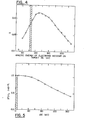
- FIG. 4i there is illustrated in graph form the analyzing power of this invention for different kinetic energies of the electrons hitting the target.
- the analyzing power is useful for electrons over a wide energy range, and is, in fact, greater than one- half its maximum value over a 120 electron volt range.
- One important aspect illustrated by Figure 4 is that the analyzing power does not change sign. As long as the sign of S does not change at a given energy, then electrons at that energy can add usefully to the signal of the polarization measurement.
- the analyzing power of the Kirschner device is represented by the shaded area. Although at optimum conditions that device performs well, it exhibits an extremely narrow functional range particularly, in contrast to that provided by this invention.
- FIG 5 there is shown the figure of merit averaged over an energy spread, AE, of an incident beam of constant total intensity.
- the average figure of merit for a beam with a 40 electron -4 volt energy spread is 1x10
- that for a beam with -4 a 120 electron volt energy spread is 0.64x10 .
- the intensity in the 120 electron volt energy sprea'd would be three times that in the 40 electron volt energy spread.
- Figure 5 illustrates the advantageous increase in signal possible in many situations because the invention can measure an electron beam with wide energy spread with high efficiency.
- the graph presented in Figure 6 illustrates the relationship between the analyzing power and the collected intensity for a nominal beam kinetic energy of 150 electron volts, where both quantities are a function of the potential on grid 22 as measured with respect to the target 26, which as detailed above, determines which energy scattered electrons are collected.
- the log of the analyzing power, log (S), is located on the right and on the left is the log of the intensity ratio, log (I/I ), o where I is the intensity scattered into two selected quadrants, e.g. 46 and 48 (see Figure 2) and I is the 0 intensity of the incident beam.
- the potential on grid 22 ranging from -140 to 0 volts comprises the abscissa.
Landscapes
- Physics & Mathematics (AREA)
- High Energy & Nuclear Physics (AREA)
- Spectroscopy & Molecular Physics (AREA)
- Life Sciences & Earth Sciences (AREA)
- General Engineering & Computer Science (AREA)
- Health & Medical Sciences (AREA)
- Engineering & Computer Science (AREA)
- General Physics & Mathematics (AREA)
- Molecular Biology (AREA)
- Analysing Materials By The Use Of Radiation (AREA)
- Measurement Of Radiation (AREA)
- Photoreceptors In Electrophotography (AREA)
- Photometry And Measurement Of Optical Pulse Characteristics (AREA)
Priority Applications (1)
| Application Number | Priority Date | Filing Date | Title |
|---|---|---|---|
| AT86304346T ATE69511T1 (de) | 1985-06-07 | 1986-06-06 | Vorrichtung und verfahren fuer die erfassung der polarisation des elektronenspins. |
Applications Claiming Priority (2)
| Application Number | Priority Date | Filing Date | Title |
|---|---|---|---|
| US742233 | 1985-06-07 | ||
| US06/742,233 US4760254A (en) | 1985-06-07 | 1985-06-07 | Apparatus and method for electron spin polarization detection |
Publications (3)
| Publication Number | Publication Date |
|---|---|
| EP0204584A2 true EP0204584A2 (de) | 1986-12-10 |
| EP0204584A3 EP0204584A3 (en) | 1988-06-15 |
| EP0204584B1 EP0204584B1 (de) | 1991-11-13 |
Family
ID=24983995
Family Applications (1)
| Application Number | Title | Priority Date | Filing Date |
|---|---|---|---|
| EP86304346A Expired - Lifetime EP0204584B1 (de) | 1985-06-07 | 1986-06-06 | Vorrichtung und Verfahren für die Erfassung der Polarisation des Elektronenspins |
Country Status (6)
| Country | Link |
|---|---|
| US (1) | US4760254A (de) |
| EP (1) | EP0204584B1 (de) |
| JP (1) | JPS61284690A (de) |
| AT (1) | ATE69511T1 (de) |
| CA (1) | CA1238990A (de) |
| DE (1) | DE3682438D1 (de) |
Cited By (1)
| Publication number | Priority date | Publication date | Assignee | Title |
|---|---|---|---|---|
| EP0490170A3 (de) * | 1990-11-30 | 1994-02-23 | Hitachi Ltd |
Families Citing this family (10)
| Publication number | Priority date | Publication date | Assignee | Title |
|---|---|---|---|---|
| JPH0754287B2 (ja) * | 1987-12-16 | 1995-06-07 | 三菱電機株式会社 | 不純物検出分析方法 |
| JP2680018B2 (ja) * | 1988-02-26 | 1997-11-19 | 株式会社日立製作所 | スピン偏極度検出器 |
| JP2760508B2 (ja) * | 1988-06-23 | 1998-06-04 | 工業技術院長 | 走査型トンネル顕微鏡 |
| FR2634061B1 (fr) * | 1988-07-06 | 1991-04-05 | Commissariat Energie Atomique | Evaporateur a bombardement electronique muni de moyens de recuperation des electrons retrodiffuses |
| GB9814775D0 (en) | 1998-07-09 | 1998-09-09 | Council Cent Lab Res Councils | Polarimeter |
| JP3383842B2 (ja) * | 2000-04-28 | 2003-03-10 | 北海道大学長 | 散乱ターゲット保持機構及び電子スピン分析器 |
| JP3757263B2 (ja) * | 2000-05-02 | 2006-03-22 | 国立大学法人 北海道大学 | 電子スピン分析器 |
| US7276694B1 (en) * | 2005-03-29 | 2007-10-02 | Kla-Tencor Technologies Corporation | Defect detection using energy spectrometer |
| JP2010054272A (ja) * | 2008-08-27 | 2010-03-11 | National Institute Of Advanced Industrial Science & Technology | スピン偏極走査電子顕微鏡 |
| RU2579186C2 (ru) * | 2010-11-17 | 2016-04-10 | Спекс Сёрфейс Нано Анализис Гмбх | Устройство детектирования спина для измерения компонент вектора спина, преобладающего в пучке частиц |
Family Cites Families (4)
| Publication number | Priority date | Publication date | Assignee | Title |
|---|---|---|---|---|
| DE2646394C2 (de) * | 1976-10-14 | 1986-12-11 | Kernforschungsanlage Jülich GmbH, 5170 Jülich | Vorrichtung zur Bestimmung des Spinpolarisationsgrades eines Elektronenstrahls |
| US4179604A (en) * | 1978-09-29 | 1979-12-18 | The United States Of America As Represented By The Secretary Of The Navy | Electron collector for forming low-loss electron images |
| CH652510A5 (en) * | 1980-12-23 | 1985-11-15 | Hans Christoph Siegmann Prof D | Method for measuring the spin polarisation of electron beams |
| US4455486A (en) * | 1981-08-12 | 1984-06-19 | Carl Rau | Method and apparatus for detecting magnetism by means of electron spin polarization measurements through dielectronic transition |
-
1985
- 1985-06-07 US US06/742,233 patent/US4760254A/en not_active Expired - Fee Related
-
1986
- 1986-05-26 CA CA000509999A patent/CA1238990A/en not_active Expired
- 1986-06-06 JP JP61131646A patent/JPS61284690A/ja active Pending
- 1986-06-06 EP EP86304346A patent/EP0204584B1/de not_active Expired - Lifetime
- 1986-06-06 AT AT86304346T patent/ATE69511T1/de not_active IP Right Cessation
- 1986-06-06 DE DE8686304346T patent/DE3682438D1/de not_active Expired - Lifetime
Cited By (1)
| Publication number | Priority date | Publication date | Assignee | Title |
|---|---|---|---|---|
| EP0490170A3 (de) * | 1990-11-30 | 1994-02-23 | Hitachi Ltd |
Also Published As
| Publication number | Publication date |
|---|---|
| EP0204584B1 (de) | 1991-11-13 |
| ATE69511T1 (de) | 1991-11-15 |
| CA1238990A (en) | 1988-07-05 |
| EP0204584A3 (en) | 1988-06-15 |
| DE3682438D1 (de) | 1991-12-19 |
| JPS61284690A (ja) | 1986-12-15 |
| US4760254A (en) | 1988-07-26 |
Similar Documents
| Publication | Publication Date | Title |
|---|---|---|
| Unguris et al. | Low‐energy diffuse scattering electron‐spin polarization analyzer | |
| Bederson et al. | Total Electron—Atom Collision Cross Sections at Low Energies—A Critical Review | |
| Busch et al. | A position-sensitive transmission time detector | |
| Gay et al. | Mott electron polarimetry | |
| US4352985A (en) | Scanning ion microscope | |
| US4236073A (en) | Scanning ion microscope | |
| EP0204584B1 (de) | Vorrichtung und Verfahren für die Erfassung der Polarisation des Elektronenspins | |
| Assmann | Ionization chambers for materials analysis with heavy ion beams | |
| US3665185A (en) | Ion scattering spectrometer with neutralization | |
| Schwestka et al. | A versatile ion beam spectrometer for studies of ion interaction with 2D materials | |
| Meinerzhagen et al. | A new setup for the investigation of swift heavy ion induced particle emission and surface modifications | |
| Dunning | Mott electron polarimetry | |
| Ross et al. | Inexpensive, quantitative hydrogen depth-profiling for surface probes | |
| Takahashi et al. | A high sensitivity electron momentum spectrometer with simultaneous detection in energy and momentum | |
| US5026988A (en) | Method and apparatus for time of flight medium energy particle scattering | |
| Goldstein et al. | X-ray spectral measurement: WDS and EDS | |
| Smith et al. | Quantitative AES: The establishment of a standard reference spectrum for the accurate determination of spectrometer transmission functions | |
| Huang et al. | Adapting a compact Mott spin polarimeter to a large commercial electron energy analyzer for spin‐polarized electron spectroscopy | |
| WO2000003267A1 (en) | Polarimeter | |
| Steckelmacher et al. | Electron spectrometer for the study of ionisation particularly near the forward direction | |
| Biswas et al. | A position sensitive ionisation chamber for measurement of fission fragments and medium mass heavy ions | |
| Fitzwilson et al. | Measurement of differential atomic collision cross sections | |
| Lifshin et al. | X-ray spectral measurement and interpretation | |
| Gisler et al. | A compact CMA spectrometer with axially integrated hybrid electron-ion gun for ISS, AES and sputter depth profile analysis | |
| Thurgate et al. | An electron spectrometer for LEED fine structure measurements |
Legal Events
| Date | Code | Title | Description |
|---|---|---|---|
| PUAI | Public reference made under article 153(3) epc to a published international application that has entered the european phase |
Free format text: ORIGINAL CODE: 0009012 |
|
| AK | Designated contracting states |
Kind code of ref document: A2 Designated state(s): AT BE CH DE FR GB IT LI LU NL SE |
|
| PUAL | Search report despatched |
Free format text: ORIGINAL CODE: 0009013 |
|
| AK | Designated contracting states |
Kind code of ref document: A3 Designated state(s): AT BE CH DE FR GB IT LI LU NL SE |
|
| 17P | Request for examination filed |
Effective date: 19881121 |
|
| 17Q | First examination report despatched |
Effective date: 19900402 |
|
| GRAA | (expected) grant |
Free format text: ORIGINAL CODE: 0009210 |
|
| AK | Designated contracting states |
Kind code of ref document: B1 Designated state(s): AT BE CH DE FR GB IT LI LU NL SE |
|
| PG25 | Lapsed in a contracting state [announced via postgrant information from national office to epo] |
Ref country code: IT Free format text: LAPSE BECAUSE OF FAILURE TO SUBMIT A TRANSLATION OF THE DESCRIPTION OR TO PAY THE FEE WITHIN THE PRE;WARNING: LAPSES OF ITALIAN PATENTS WITH EFFECTIVE DATE BEFORE 2007 MAY HAVE OCCURRED AT ANY TIME BEFORE 2007. THE CORRECT EFFECTIVE DATE MAY BE DIFFERENT FROM THE ONE RECORDED.SCRIBED TIME-LIMIT Effective date: 19911113 Ref country code: AT Effective date: 19911113 Ref country code: LI Effective date: 19911113 Ref country code: CH Effective date: 19911113 Ref country code: NL Effective date: 19911113 Ref country code: BE Effective date: 19911113 Ref country code: SE Effective date: 19911113 |
|
| REF | Corresponds to: |
Ref document number: 69511 Country of ref document: AT Date of ref document: 19911115 Kind code of ref document: T |
|
| REF | Corresponds to: |
Ref document number: 3682438 Country of ref document: DE Date of ref document: 19911219 |
|
| REG | Reference to a national code |
Ref country code: CH Ref legal event code: PL |
|
| ET | Fr: translation filed | ||
| NLV1 | Nl: lapsed or annulled due to failure to fulfill the requirements of art. 29p and 29m of the patents act | ||
| PG25 | Lapsed in a contracting state [announced via postgrant information from national office to epo] |
Ref country code: LU Free format text: LAPSE BECAUSE OF NON-PAYMENT OF DUE FEES Effective date: 19920630 |
|
| PLBE | No opposition filed within time limit |
Free format text: ORIGINAL CODE: 0009261 |
|
| STAA | Information on the status of an ep patent application or granted ep patent |
Free format text: STATUS: NO OPPOSITION FILED WITHIN TIME LIMIT |
|
| 26N | No opposition filed | ||
| REG | Reference to a national code |
Ref country code: FR Ref legal event code: TP |
|
| REG | Reference to a national code |
Ref country code: GB Ref legal event code: 732E |
|
| PGFP | Annual fee paid to national office [announced via postgrant information from national office to epo] |
Ref country code: FR Payment date: 19980520 Year of fee payment: 13 |
|
| PGFP | Annual fee paid to national office [announced via postgrant information from national office to epo] |
Ref country code: GB Payment date: 19980526 Year of fee payment: 13 |
|
| PGFP | Annual fee paid to national office [announced via postgrant information from national office to epo] |
Ref country code: DE Payment date: 19980527 Year of fee payment: 13 |
|
| PG25 | Lapsed in a contracting state [announced via postgrant information from national office to epo] |
Ref country code: GB Free format text: LAPSE BECAUSE OF NON-PAYMENT OF DUE FEES Effective date: 19990606 |
|
| PG25 | Lapsed in a contracting state [announced via postgrant information from national office to epo] |
Ref country code: FR Free format text: THE PATENT HAS BEEN ANNULLED BY A DECISION OF A NATIONAL AUTHORITY Effective date: 19990630 |
|
| GBPC | Gb: european patent ceased through non-payment of renewal fee |
Effective date: 19990606 |
|
| PG25 | Lapsed in a contracting state [announced via postgrant information from national office to epo] |
Ref country code: DE Free format text: LAPSE BECAUSE OF NON-PAYMENT OF DUE FEES Effective date: 20000503 |
|
| REG | Reference to a national code |
Ref country code: FR Ref legal event code: ST |