EP0201916A2 - Bonding method of semiconductor device - Google Patents
Bonding method of semiconductor device Download PDFInfo
- Publication number
- EP0201916A2 EP0201916A2 EP86106546A EP86106546A EP0201916A2 EP 0201916 A2 EP0201916 A2 EP 0201916A2 EP 86106546 A EP86106546 A EP 86106546A EP 86106546 A EP86106546 A EP 86106546A EP 0201916 A2 EP0201916 A2 EP 0201916A2
- Authority
- EP
- European Patent Office
- Prior art keywords
- semiconductor device
- bonding method
- accordance
- bumps
- photo
- Prior art date
- Legal status (The legal status is an assumption and is not a legal conclusion. Google has not performed a legal analysis and makes no representation as to the accuracy of the status listed.)
- Withdrawn
Links
- 238000000034 method Methods 0.000 title claims abstract description 32
- 239000004065 semiconductor Substances 0.000 title claims abstract description 32
- 238000007747 plating Methods 0.000 claims abstract description 16
- BASFCYQUMIYNBI-UHFFFAOYSA-N platinum Chemical compound [Pt] BASFCYQUMIYNBI-UHFFFAOYSA-N 0.000 claims description 22
- PCHJSUWPFVWCPO-UHFFFAOYSA-N gold Chemical compound [Au] PCHJSUWPFVWCPO-UHFFFAOYSA-N 0.000 claims description 20
- 239000010931 gold Substances 0.000 claims description 20
- 229910052737 gold Inorganic materials 0.000 claims description 20
- 229910052697 platinum Inorganic materials 0.000 claims description 11
- RTAQQCXQSZGOHL-UHFFFAOYSA-N Titanium Chemical compound [Ti] RTAQQCXQSZGOHL-UHFFFAOYSA-N 0.000 claims description 9
- 239000010936 titanium Substances 0.000 claims description 9
- 229910052719 titanium Inorganic materials 0.000 claims description 9
- 238000007906 compression Methods 0.000 claims description 8
- 239000000758 substrate Substances 0.000 claims description 6
- 239000003093 cationic surfactant Substances 0.000 claims description 4
- 238000000151 deposition Methods 0.000 claims description 4
- 239000002904 solvent Substances 0.000 claims description 4
- 238000004544 sputter deposition Methods 0.000 claims description 3
- 239000004094 surface-active agent Substances 0.000 claims description 3
- 238000004140 cleaning Methods 0.000 claims description 2
- 238000010438 heat treatment Methods 0.000 claims description 2
- 239000010408 film Substances 0.000 claims 9
- GRYLNZFGIOXLOG-UHFFFAOYSA-N Nitric acid Chemical compound O[N+]([O-])=O GRYLNZFGIOXLOG-UHFFFAOYSA-N 0.000 claims 1
- 229910017604 nitric acid Inorganic materials 0.000 claims 1
- 239000010409 thin film Substances 0.000 claims 1
- 238000001771 vacuum deposition Methods 0.000 claims 1
- 229920002120 photoresistant polymer Polymers 0.000 description 10
- ATJFFYVFTNAWJD-UHFFFAOYSA-N Tin Chemical compound [Sn] ATJFFYVFTNAWJD-UHFFFAOYSA-N 0.000 description 3
- 238000005406 washing Methods 0.000 description 3
- 239000000374 eutectic mixture Substances 0.000 description 2
- 238000004299 exfoliation Methods 0.000 description 2
- 239000011521 glass Substances 0.000 description 2
- XLYOFNOQVPJJNP-UHFFFAOYSA-N water Substances O XLYOFNOQVPJJNP-UHFFFAOYSA-N 0.000 description 2
- 241000416536 Euproctis pseudoconspersa Species 0.000 description 1
- PNEYBMLMFCGWSK-UHFFFAOYSA-N aluminium oxide Inorganic materials [O-2].[O-2].[O-2].[Al+3].[Al+3] PNEYBMLMFCGWSK-UHFFFAOYSA-N 0.000 description 1
- 150000001408 amides Chemical class 0.000 description 1
- -1 amine-oxides Chemical class 0.000 description 1
- 150000001412 amines Chemical class 0.000 description 1
- 239000007864 aqueous solution Substances 0.000 description 1
- 239000011248 coating agent Substances 0.000 description 1
- 238000000576 coating method Methods 0.000 description 1
- 238000009713 electroplating Methods 0.000 description 1
- 238000005530 etching Methods 0.000 description 1
- 238000004519 manufacturing process Methods 0.000 description 1
- 239000000463 material Substances 0.000 description 1
- 229910052751 metal Inorganic materials 0.000 description 1
- 239000002184 metal Substances 0.000 description 1
- 239000003960 organic solvent Substances 0.000 description 1
- 150000003242 quaternary ammonium salts Chemical class 0.000 description 1
- 230000009466 transformation Effects 0.000 description 1
- 238000007738 vacuum evaporation Methods 0.000 description 1
Images


Classifications
-
- H—ELECTRICITY
- H01—ELECTRIC ELEMENTS
- H01L—SEMICONDUCTOR DEVICES NOT COVERED BY CLASS H10
- H01L24/00—Arrangements for connecting or disconnecting semiconductor or solid-state bodies; Methods or apparatus related thereto
- H01L24/01—Means for bonding being attached to, or being formed on, the surface to be connected, e.g. chip-to-package, die-attach, "first-level" interconnects; Manufacturing methods related thereto
- H01L24/10—Bump connectors ; Manufacturing methods related thereto
- H01L24/12—Structure, shape, material or disposition of the bump connectors prior to the connecting process
- H01L24/13—Structure, shape, material or disposition of the bump connectors prior to the connecting process of an individual bump connector
-
- H—ELECTRICITY
- H01—ELECTRIC ELEMENTS
- H01L—SEMICONDUCTOR DEVICES NOT COVERED BY CLASS H10
- H01L24/00—Arrangements for connecting or disconnecting semiconductor or solid-state bodies; Methods or apparatus related thereto
- H01L24/80—Methods for connecting semiconductor or other solid state bodies using means for bonding being attached to, or being formed on, the surface to be connected
- H01L24/81—Methods for connecting semiconductor or other solid state bodies using means for bonding being attached to, or being formed on, the surface to be connected using a bump connector
-
- H—ELECTRICITY
- H01—ELECTRIC ELEMENTS
- H01L—SEMICONDUCTOR DEVICES NOT COVERED BY CLASS H10
- H01L2224/00—Indexing scheme for arrangements for connecting or disconnecting semiconductor or solid-state bodies and methods related thereto as covered by H01L24/00
- H01L2224/01—Means for bonding being attached to, or being formed on, the surface to be connected, e.g. chip-to-package, die-attach, "first-level" interconnects; Manufacturing methods related thereto
- H01L2224/02—Bonding areas; Manufacturing methods related thereto
- H01L2224/04—Structure, shape, material or disposition of the bonding areas prior to the connecting process
- H01L2224/05—Structure, shape, material or disposition of the bonding areas prior to the connecting process of an individual bonding area
- H01L2224/0554—External layer
- H01L2224/05599—Material
- H01L2224/056—Material with a principal constituent of the material being a metal or a metalloid, e.g. boron [B], silicon [Si], germanium [Ge], arsenic [As], antimony [Sb], tellurium [Te] and polonium [Po], and alloys thereof
- H01L2224/05638—Material with a principal constituent of the material being a metal or a metalloid, e.g. boron [B], silicon [Si], germanium [Ge], arsenic [As], antimony [Sb], tellurium [Te] and polonium [Po], and alloys thereof the principal constituent melting at a temperature of greater than or equal to 950°C and less than 1550°C
- H01L2224/05644—Gold [Au] as principal constituent
-
- H—ELECTRICITY
- H01—ELECTRIC ELEMENTS
- H01L—SEMICONDUCTOR DEVICES NOT COVERED BY CLASS H10
- H01L2224/00—Indexing scheme for arrangements for connecting or disconnecting semiconductor or solid-state bodies and methods related thereto as covered by H01L24/00
- H01L2224/01—Means for bonding being attached to, or being formed on, the surface to be connected, e.g. chip-to-package, die-attach, "first-level" interconnects; Manufacturing methods related thereto
- H01L2224/10—Bump connectors; Manufacturing methods related thereto
- H01L2224/12—Structure, shape, material or disposition of the bump connectors prior to the connecting process
- H01L2224/13—Structure, shape, material or disposition of the bump connectors prior to the connecting process of an individual bump connector
- H01L2224/13001—Core members of the bump connector
- H01L2224/13099—Material
-
- H—ELECTRICITY
- H01—ELECTRIC ELEMENTS
- H01L—SEMICONDUCTOR DEVICES NOT COVERED BY CLASS H10
- H01L2224/00—Indexing scheme for arrangements for connecting or disconnecting semiconductor or solid-state bodies and methods related thereto as covered by H01L24/00
- H01L2224/80—Methods for connecting semiconductor or other solid state bodies using means for bonding being attached to, or being formed on, the surface to be connected
- H01L2224/81—Methods for connecting semiconductor or other solid state bodies using means for bonding being attached to, or being formed on, the surface to be connected using a bump connector
- H01L2224/818—Bonding techniques
- H01L2224/81801—Soldering or alloying
-
- H—ELECTRICITY
- H01—ELECTRIC ELEMENTS
- H01L—SEMICONDUCTOR DEVICES NOT COVERED BY CLASS H10
- H01L2924/00—Indexing scheme for arrangements or methods for connecting or disconnecting semiconductor or solid-state bodies as covered by H01L24/00
- H01L2924/01—Chemical elements
- H01L2924/01006—Carbon [C]
-
- H—ELECTRICITY
- H01—ELECTRIC ELEMENTS
- H01L—SEMICONDUCTOR DEVICES NOT COVERED BY CLASS H10
- H01L2924/00—Indexing scheme for arrangements or methods for connecting or disconnecting semiconductor or solid-state bodies as covered by H01L24/00
- H01L2924/01—Chemical elements
- H01L2924/01022—Titanium [Ti]
-
- H—ELECTRICITY
- H01—ELECTRIC ELEMENTS
- H01L—SEMICONDUCTOR DEVICES NOT COVERED BY CLASS H10
- H01L2924/00—Indexing scheme for arrangements or methods for connecting or disconnecting semiconductor or solid-state bodies as covered by H01L24/00
- H01L2924/01—Chemical elements
- H01L2924/01033—Arsenic [As]
-
- H—ELECTRICITY
- H01—ELECTRIC ELEMENTS
- H01L—SEMICONDUCTOR DEVICES NOT COVERED BY CLASS H10
- H01L2924/00—Indexing scheme for arrangements or methods for connecting or disconnecting semiconductor or solid-state bodies as covered by H01L24/00
- H01L2924/01—Chemical elements
- H01L2924/0105—Tin [Sn]
-
- H—ELECTRICITY
- H01—ELECTRIC ELEMENTS
- H01L—SEMICONDUCTOR DEVICES NOT COVERED BY CLASS H10
- H01L2924/00—Indexing scheme for arrangements or methods for connecting or disconnecting semiconductor or solid-state bodies as covered by H01L24/00
- H01L2924/01—Chemical elements
- H01L2924/01078—Platinum [Pt]
-
- H—ELECTRICITY
- H01—ELECTRIC ELEMENTS
- H01L—SEMICONDUCTOR DEVICES NOT COVERED BY CLASS H10
- H01L2924/00—Indexing scheme for arrangements or methods for connecting or disconnecting semiconductor or solid-state bodies as covered by H01L24/00
- H01L2924/01—Chemical elements
- H01L2924/01079—Gold [Au]
-
- H—ELECTRICITY
- H01—ELECTRIC ELEMENTS
- H01L—SEMICONDUCTOR DEVICES NOT COVERED BY CLASS H10
- H01L2924/00—Indexing scheme for arrangements or methods for connecting or disconnecting semiconductor or solid-state bodies as covered by H01L24/00
- H01L2924/01—Chemical elements
- H01L2924/01082—Lead [Pb]
-
- H—ELECTRICITY
- H01—ELECTRIC ELEMENTS
- H01L—SEMICONDUCTOR DEVICES NOT COVERED BY CLASS H10
- H01L2924/00—Indexing scheme for arrangements or methods for connecting or disconnecting semiconductor or solid-state bodies as covered by H01L24/00
- H01L2924/013—Alloys
- H01L2924/0132—Binary Alloys
- H01L2924/01322—Eutectic Alloys, i.e. obtained by a liquid transforming into two solid phases
-
- Y—GENERAL TAGGING OF NEW TECHNOLOGICAL DEVELOPMENTS; GENERAL TAGGING OF CROSS-SECTIONAL TECHNOLOGIES SPANNING OVER SEVERAL SECTIONS OF THE IPC; TECHNICAL SUBJECTS COVERED BY FORMER USPC CROSS-REFERENCE ART COLLECTIONS [XRACs] AND DIGESTS
- Y10—TECHNICAL SUBJECTS COVERED BY FORMER USPC
- Y10T—TECHNICAL SUBJECTS COVERED BY FORMER US CLASSIFICATION
- Y10T29/00—Metal working
- Y10T29/49—Method of mechanical manufacture
- Y10T29/49002—Electrical device making
- Y10T29/49117—Conductor or circuit manufacturing
- Y10T29/49121—Beam lead frame or beam lead device
Definitions
- This invention relates to a bonding method of semiconductor device.
- the former necessitates difficult process for forming the gold bumps directly on the semiconductor element, and the former method is expensive. Therefore, it is not used in conventional I.C chip.
- the latter does not necessitate difficult process for forming the gold bumps directly on the semiconductor element, because the gold bumps are formed on the inner leads, and hence the latter costs cheap. Therefore, it is used in conventional I.C chip.
- a prior method for forming the gold bumps is illustrated.
- a platinum film 103 is formed over a titanium film 102 formed on an insulating substrate 101. Further, as shown in FIG.1, an organic photo resist 105 is applied over the platinum film 103.
- the organic photo resist 105 is patterned by using a photo mask, so as to make the dummy wafer having openings 107 for forming the bumps.
- the bumps 106 of gold are formed by plating by using the titanium film 102 and the platinum film 103 as the plating electrode.
- the organic photo-resist is removed by using organic solvent so as to prevent softening or transformation of the organic photo-resist 105 and to prevent adhering of the organic photo-resist 105 to the gold bumps 106 or the tool for thermo-compression bonding. Such adhering has a bad influence upon a step for bonding the gold bumps to the bonding pads of the semiconductor element.
- the gold bumps 106 are transferred to the inner leads of the film carrier.
- a first bonding indicates the bonding of the gold bumps 106 onto the inner leads of the film carrier.
- a second bonding indicates the bonding of the gold bumps 106 bonded on the inner leads onto the bonding pads of the semiconductor element,
- the removing step must be necessary before the first bonding, because the organic photo-resist 105 is used as mask for plating. Further, it necessitates repetition of the above-mentioned steps after the application step of the organic photo resist 105. Therefore, the prior method was expensive in the material cost of the organic photo resist 105, in the wages and in manufacturing apparatuses.
- a principal object of this invention is to provide a bonding method of semiconductor device having no removing step of the photo-resist as a mask for plating, and to provide dummy wafer capable of repeated uses.
- Bonding method of semiconductor device in accordance with the present invention comprises the steps of
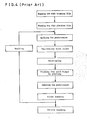
- FIGs. 1 to 3 is a cross-sectional view for showing the prior bonding method of semiconductor device.
- FIG.4 is a flow chart of the prior bonding method of semiconductor device.
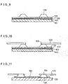
- FIGs. 5 to 11 is a cross-sectional view for showing the bonding method of semiconductor device in accordance with the present invention.
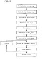
- FIG.12 is a flow chart of the bonding method of semiconductor device in accordance with the present invention.
- a dummy wafer is a medium for forming the bumps 106 thereon by electrolytic plating.
- the dummy wafer that which has a good conductivity at least in their surface, has flat surface and has appropriate adhesion and exfoliation characteristics to the bumps, is suitable.
- such dummy wafer can be mentioned that, which comprises a glass substrate having double conductive layer of a titanium film and a platinum film thereon, a glazed alumina substrate having a double- layered thin conductive layers of titanium film and a platinum film thereon, or polished metal plate whereon unnecessary parts are covered by an insulative coating.
- a platinum film 103 is formed on a titanium film 102 formed on a insulating substrate 101, for example, a glass dummy substrate.
- the underlying titanium film 102 is formed for improving the adhesion of the platinum film 103.
- the organic photo resist 105 is applied on the platinum film 103.
- a heat-resistive insulating layer 110 of Si0 2 is deposited all over the surface of the dummy wafer by sputtering method. From 5000 to 20000 ⁇ thickness of the photo-resist pattern 4 is desirable. About 14000 A thickness particularly desirable for the photo-resist. From 2000 A to 10000 A thickness of the Sio 2 film 5 is desirable. About 7000 A thickness is particularly desirable for the Si0 2 film 5. Instead of the sputtering, vacuum evaporation can be used. By heating the dummy wafer at about 500°C, the organic photo-resist 105a are destroyed by fire, so the resistive insulating layers 110a on the organic photo resists 105 a are also removed.
- the dummy wafer having the heat-resistive insulating layer as a mask for plating is provided.
- the dummy wafer has the openings 107.
- solvent washing, alkaline treating or treating by can be used.
- the dummy wafer is steeped in cationic surfactant of 5% as solvent for 5 minutes and dried after washing in water. This solvent cleaning is carried out for improving the exfoliation of the bumps 106 from the dummy wafer.
- the bumps 106 of gold are formed with 20 ⁇ m thickness by plating by using the titanium film 102 and the platinum film 103 as the plating electrode.
- the gold bumps 106 are transferred to the tin plated inner leads 120 of the film carried by using a known thermo-compression bonding tool (not shown).
- This step is called first bonding step.
- suitable temperature for the lead 120 is such a temperature that at which eutectic mixture of gold of the bump 106 and the tin of the inner leads 120 is formed.
- thermo-compression bonding and/or ultrasonic bonding can be used.
- the bumps 106 of the inner leads 120 are bonded to bonding pads 140 of the semiconductor element 130 by using thermo-compression bonding tool (not shown).
- This step is called second bonding step.
- suitable temperature of the bumps 106 is such a temperature that at which the eutectic mixture of gold of the bump 106 and the gold of the bonding pad 140 is formed.
- the same gold bumps 106 can be formed again by again plating gold after removing the remaining bumps by washing in water. According to the inventor's experimental research, the dummy wafer can be used for forming the bumps 106 without hindrance even after 20 times repeating of plating and first bonding.
- One member of amines, amine-oxides, amides, quaternary ammonium salts or the like is suitable for the cationic surfactant.
- An aqueous solution of the cationic surfactant having the density of from several % to ten and several % is suitable.
- the treatment of the surface- active agent may be carried out before applying the photo resist 105.
- the bonding method in accordance with the present invention does not necessitate the removing step of the mask for plating, because the heat-resistive insulating layer is used for the mask for plating. Therefore, the heat-resistive insulating layer can be repeatedly used.
- the etching step is not necessary because the heat-resistive insulating layer can be patterned by destroying the organic photo resist 105a by fire.
Abstract
Description
- This invention relates to a bonding method of semiconductor device.
- There are two bonding methods of semiconductor device by using film carrier. One is method that tin plated inner leads of the film carrier are thermo-compression bonded with gold bumps previously formed on bonding pads of the semiconductor element. The other is a method that the gold bumps previously formed on the inner leads are thermp-compression bonded to the bonding pads of the semiconductor element.
- The former necessitates difficult process for forming the gold bumps directly on the semiconductor element, and the former method is expensive. Therefore, it is not used in conventional I.C chip. The latter does not necessitate difficult process for forming the gold bumps directly on the semiconductor element, because the gold bumps are formed on the inner leads, and hence the latter costs cheap. Therefore, it is used in conventional I.C chip.
- Referring to FIGs. 1 to 3, a prior method for forming the gold bumps is illustrated. A
platinum film 103 is formed over atitanium film 102 formed on aninsulating substrate 101. Further, as shown in FIG.1, anorganic photo resist 105 is applied over theplatinum film 103. - Then as shown in FIG.2, the
organic photo resist 105 is patterned by using a photo mask, so as to make the dummywafer having openings 107 for forming the bumps. - Then as shown in FIG.3, the
bumps 106 of gold are formed by plating by using thetitanium film 102 and theplatinum film 103 as the plating electrode. In the next place, the organic photo-resist is removed by using organic solvent so as to prevent softening or transformation of the organic photo-resist 105 and to prevent adhering of the organic photo-resist 105 to thegold bumps 106 or the tool for thermo-compression bonding. Such adhering has a bad influence upon a step for bonding the gold bumps to the bonding pads of the semiconductor element. - Then, the
gold bumps 106 are transferred to the inner leads of the film carrier. - As shown in FIG.4, in the prior method, the organic photo resist must be again applied, patterned and removed for again forming of the
gold bumps 106. In FIG.4, a first bonding indicates the bonding of thegold bumps 106 onto the inner leads of the film carrier. A second bonding indicates the bonding of thegold bumps 106 bonded on the inner leads onto the bonding pads of the semiconductor element, - As mentioned above, in the prior method the removing step must be necessary before the first bonding, because the organic photo-
resist 105 is used as mask for plating. Further, it necessitates repetition of the above-mentioned steps after the application step of the organic photo resist 105. Therefore, the prior method was expensive in the material cost of the organic photo resist 105, in the wages and in manufacturing apparatuses. OBJECT AND SUMMARY OF THE INVENTION - A principal object of this invention is to provide a bonding method of semiconductor device having no removing step of the photo-resist as a mask for plating, and to provide dummy wafer capable of repeated uses.
- Bonding method of semiconductor device in accordance with the present invention comprises the steps of
- forming a photo-resist film having predetermined pattern on a conductive layer formed on a dummy wafer,
- depositing a heat-resisting insulating layer all over the surface of said dummy wafer,
- removing said photo-resist film together with said heat-resistive insulating layer deposited thereon, thereby forming openings,
- forming bumps on said openings by plating using said heat-resisting insulating layer as a mask and using said conductive layer as a plating electrode,
- transferring said bumps to inner leads from said dummy wafer, and
- thermo-compression bonding the said bumps of the inner leads to bonding pads of the semiconductor element. BRIEF DESCRIPTION OF THE DRAWINGS
- FIGs. 1 to 3 is a cross-sectional view for showing the prior bonding method of semiconductor device.
- FIG.4 is a flow chart of the prior bonding method of semiconductor device.
- FIGs. 5 to 11 is a cross-sectional view for showing the bonding method of semiconductor device in accordance with the present invention.
- FIG.12 is a flow chart of the bonding method of semiconductor device in accordance with the present invention.
- In the present invention, a dummy wafer is a medium for forming the
bumps 106 thereon by electrolytic plating. As the dummy wafer, that which has a good conductivity at least in their surface, has flat surface and has appropriate adhesion and exfoliation characteristics to the bumps, is suitable. For example, such dummy wafer can be mentioned that, which comprises a glass substrate having double conductive layer of a titanium film and a platinum film thereon, a glazed alumina substrate having a double- layered thin conductive layers of titanium film and a platinum film thereon, or polished metal plate whereon unnecessary parts are covered by an insulative coating. - A preferred embodiment is described referring to FIGs. 5 to 11. Referring to FIG.5, a
platinum film 103 is formed on atitanium film 102 formed on ainsulating substrate 101, for example, a glass dummy substrate. Theunderlying titanium film 102 is formed for improving the adhesion of theplatinum film 103. Theorganic photo resist 105 is applied on theplatinum film 103. - Then as shown in FIG.6, after a pre-baking of the organic photo resist 105, light exposure is made by using a photo mask, so as to make the
projections 105a for forming anopenings 107. Then, a post-baking is carried out. - Next as shown in FIG.7, a heat-
resistive insulating layer 110 of Si02 is deposited all over the surface of the dummy wafer by sputtering method. From 5000 to 20000 Å thickness of the photo-resist pattern 4 is desirable. About 14000 A thickness particularly desirable for the photo-resist. From 2000 A to 10000 A thickness of the Sio2 film 5 is desirable. About 7000 A thickness is particularly desirable for the Si02 film 5. Instead of the sputtering, vacuum evaporation can be used. By heating the dummy wafer at about 500°C, the organic photo-resist 105a are destroyed by fire, so the resistiveinsulating layers 110a on the organic photo resists 105 a are also removed. Therefore, as shown in FIG.8, the dummy wafer having the heat-resistive insulating layer as a mask for plating is provided. The dummy wafer has theopenings 107. Instead of the destroying by fire, solvent washing, alkaline treating or treating by can be used. - Then, the dummy wafer is steeped in cationic surfactant of 5% as solvent for 5 minutes and dried after washing in water. This solvent cleaning is carried out for improving the exfoliation of the
bumps 106 from the dummy wafer. - Next as shown in FIG.9, the
bumps 106 of gold are formed with 20 µm thickness by plating by using thetitanium film 102 and theplatinum film 103 as the plating electrode. Then as shown in FIG.10, thegold bumps 106 are transferred to the tin platedinner leads 120 of the film carried by using a known thermo-compression bonding tool (not shown). This step is called first bonding step. In the first bonding step, suitable temperature for thelead 120 is such a temperature that at which eutectic mixture of gold of thebump 106 and the tin of theinner leads 120 is formed. For the transferring, thermo-compression bonding and/or ultrasonic bonding can be used. - Next as shown in FIG.11, the
bumps 106 of the inner leads 120 are bonded tobonding pads 140 of thesemiconductor element 130 by using thermo-compression bonding tool (not shown). This step is called second bonding step. In the second bonding step, suitable temperature of thebumps 106 is such a temperature that at which the eutectic mixture of gold of thebump 106 and the gold of thebonding pad 140 is formed. - The same gold bumps 106 can be formed again by again plating gold after removing the remaining bumps by washing in water. According to the inventor's experimental research, the dummy wafer can be used for forming the
bumps 106 without hindrance even after 20 times repeating of plating and first bonding. - One member of amines, amine-oxides, amides, quaternary ammonium salts or the like is suitable for the cationic surfactant. An aqueous solution of the cationic surfactant having the density of from several % to ten and several % is suitable. The treatment of the surface- active agent may be carried out before applying the photo resist 105.
- As has been described above, the bonding method in accordance with the present invention does not necessitate the removing step of the mask for plating, because the heat-resistive insulating layer is used for the mask for plating. Therefore, the heat-resistive insulating layer can be repeatedly used. In the present invention, the etching step is not necessary because the heat-resistive insulating layer can be patterned by destroying the organic photo resist 105a by fire.
Claims (12)
Applications Claiming Priority (2)
| Application Number | Priority Date | Filing Date | Title |
|---|---|---|---|
| JP60103021A JPS61260648A (en) | 1985-05-15 | 1985-05-15 | Packaging method for semiconductor device |
| JP103021/85 | 1985-05-15 |
Publications (2)
| Publication Number | Publication Date |
|---|---|
| EP0201916A2 true EP0201916A2 (en) | 1986-11-20 |
| EP0201916A3 EP0201916A3 (en) | 1988-08-24 |
Family
ID=14342990
Family Applications (1)
| Application Number | Title | Priority Date | Filing Date |
|---|---|---|---|
| EP86106546A Withdrawn EP0201916A3 (en) | 1985-05-15 | 1986-05-14 | Bonding method of semiconductor device |
Country Status (4)
| Country | Link |
|---|---|
| US (1) | US4676864A (en) |
| EP (1) | EP0201916A3 (en) |
| JP (1) | JPS61260648A (en) |
| CA (1) | CA1240410A (en) |
Families Citing this family (3)
| Publication number | Priority date | Publication date | Assignee | Title |
|---|---|---|---|---|
| US4842662A (en) * | 1988-06-01 | 1989-06-27 | Hewlett-Packard Company | Process for bonding integrated circuit components |
| US4963225A (en) * | 1989-10-20 | 1990-10-16 | Tektronix, Inc. | Method of fabricating a contact device |
| JP3494940B2 (en) * | 1999-12-20 | 2004-02-09 | シャープ株式会社 | Tape carrier type semiconductor device, manufacturing method thereof, and liquid crystal module using the same |
Citations (4)
| Publication number | Priority date | Publication date | Assignee | Title |
|---|---|---|---|---|
| JPS59147451A (en) * | 1983-02-14 | 1984-08-23 | Matsushita Electric Ind Co Ltd | Mounting method of semiconductor element |
| JPS6086854A (en) * | 1983-10-19 | 1985-05-16 | Matsushita Electric Ind Co Ltd | Bump electrode forming substrate and manufacture thereof |
| EP0147576A1 (en) * | 1983-11-25 | 1985-07-10 | International Business Machines Corporation | Process for forming elongated solder connections between a semiconductor device and a supporting substrate |
| JPS6290957A (en) * | 1985-10-17 | 1987-04-25 | Matsushita Electric Ind Co Ltd | Manufacture of semiconductor device |
Family Cites Families (3)
| Publication number | Priority date | Publication date | Assignee | Title |
|---|---|---|---|---|
| US3751292A (en) * | 1971-08-20 | 1973-08-07 | Motorola Inc | Multilayer metallization system |
| US4070230A (en) * | 1974-07-04 | 1978-01-24 | Siemens Aktiengesellschaft | Semiconductor component with dielectric carrier and its manufacture |
| US4310570A (en) * | 1979-12-20 | 1982-01-12 | Eaton Corporation | Field-effect transistors with micron and submicron gate lengths |
-
1985
- 1985-05-15 JP JP60103021A patent/JPS61260648A/en active Pending
-
1986
- 1986-05-14 US US06/863,152 patent/US4676864A/en not_active Expired - Lifetime
- 1986-05-14 CA CA000509180A patent/CA1240410A/en not_active Expired
- 1986-05-14 EP EP86106546A patent/EP0201916A3/en not_active Withdrawn
Patent Citations (4)
| Publication number | Priority date | Publication date | Assignee | Title |
|---|---|---|---|---|
| JPS59147451A (en) * | 1983-02-14 | 1984-08-23 | Matsushita Electric Ind Co Ltd | Mounting method of semiconductor element |
| JPS6086854A (en) * | 1983-10-19 | 1985-05-16 | Matsushita Electric Ind Co Ltd | Bump electrode forming substrate and manufacture thereof |
| EP0147576A1 (en) * | 1983-11-25 | 1985-07-10 | International Business Machines Corporation | Process for forming elongated solder connections between a semiconductor device and a supporting substrate |
| JPS6290957A (en) * | 1985-10-17 | 1987-04-25 | Matsushita Electric Ind Co Ltd | Manufacture of semiconductor device |
Non-Patent Citations (4)
| Title |
|---|
| IBM TECHNICAL DISCLOSURE BULLETIN, vol. 17, no. 9, February 1975, page 2590, New York, US; R.W. NOTH et al.: "Solder transfer technique" * |
| PATENT ABSTRACTS OF JAPAN, vol. 11, no. 292 (E-543)[2739], 19th September 1987; & JP-A-62 090 957 (MATSUSHITA ELECTRIC IND. CO. LTD) 25-04-1987 * |
| PATENT ABSTRACTS OF JAPAN, vol. 8, no. 277 (E-285)[1714], 18th December 1984; & JP-A-59 147 451 (MATSUSHITA DENKI SANGYO K.K.) 23-08-1984 * |
| PATENT ABSTRACTS OF JAPAN, vol. 9, no. 230 (E-343)[1953], 17th September 1985; & JP-A-60 086 854 (MATSUSHITA DENKI SANGYO K.K.) 16-05-1985 * |
Also Published As
| Publication number | Publication date |
|---|---|
| EP0201916A3 (en) | 1988-08-24 |
| US4676864A (en) | 1987-06-30 |
| CA1240410A (en) | 1988-08-09 |
| JPS61260648A (en) | 1986-11-18 |
Similar Documents
| Publication | Publication Date | Title |
|---|---|---|
| JP3554685B2 (en) | Method of bonding IC chip to support substrate | |
| US5118584A (en) | Method of producing microbump circuits for flip chip mounting | |
| JP2003338516A (en) | Semiconductor device and method of manufacturing the same | |
| US4387116A (en) | Conditioner for adherence of nickel to a tin oxide surface | |
| US4676864A (en) | Bonding method of semiconductor device | |
| JP2811741B2 (en) | Method for manufacturing semiconductor device | |
| JPH0357617B2 (en) | ||
| US4067100A (en) | Method of making a semiconductor device | |
| JPH07201922A (en) | Method for forming solder bump on board | |
| JPS6348427B2 (en) | ||
| JP2895568B2 (en) | Electric circuit members | |
| JPH0661233A (en) | Manufacture of semiconductor device | |
| JPH09232321A (en) | Bump electrode and manufacture thereof | |
| JPH02267941A (en) | Formation of protruding electrode | |
| JPS61251153A (en) | Formation of bump of semiconductor device | |
| JPS63119551A (en) | Forming method of patterned metal film | |
| KR100237671B1 (en) | Semiconductor apparatus fabrication method | |
| JP3218957B2 (en) | Semiconductor device and manufacturing method thereof | |
| JP2002289634A (en) | Semiconductor device and manufacturing method thereof | |
| JPS5893333A (en) | Manufacture of semiconductor device | |
| JPS61121963A (en) | Thermal head | |
| JPS6019661B2 (en) | Electrode formation method | |
| JPH04174522A (en) | Manufacture of bump formation plating of semiconductor device | |
| JPS5863151A (en) | Forming method for electrode wirings | |
| JPH031832B2 (en) |
Legal Events
| Date | Code | Title | Description |
|---|---|---|---|
| PUAI | Public reference made under article 153(3) epc to a published international application that has entered the european phase |
Free format text: ORIGINAL CODE: 0009012 |
|
| AK | Designated contracting states |
Kind code of ref document: A2 Designated state(s): DE FR GB |
|
| PUAL | Search report despatched |
Free format text: ORIGINAL CODE: 0009013 |
|
| AK | Designated contracting states |
Kind code of ref document: A3 Designated state(s): DE FR GB |
|
| STAA | Information on the status of an ep patent application or granted ep patent |
Free format text: STATUS: THE APPLICATION IS DEEMED TO BE WITHDRAWN |
|
| 18D | Application deemed to be withdrawn |
Effective date: 19890225 |
|
| RIN1 | Information on inventor provided before grant (corrected) |
Inventor name: KITAYAMA, YOSHIFUMI Inventor name: MAEDA, YUKIO Inventor name: MURAKAMI, SHUICHI |