EP0200600B1 - Bei hoher Frequenz arbeitende Transistorbasissteuerschaltung - Google Patents
Bei hoher Frequenz arbeitende Transistorbasissteuerschaltung Download PDFInfo
- Publication number
- EP0200600B1 EP0200600B1 EP86400668A EP86400668A EP0200600B1 EP 0200600 B1 EP0200600 B1 EP 0200600B1 EP 86400668 A EP86400668 A EP 86400668A EP 86400668 A EP86400668 A EP 86400668A EP 0200600 B1 EP0200600 B1 EP 0200600B1
- Authority
- EP
- European Patent Office
- Prior art keywords
- circuit
- capacitor
- switch
- power transistor
- transistor
- Prior art date
- Legal status (The legal status is an assumption and is not a legal conclusion. Google has not performed a legal analysis and makes no representation as to the accuracy of the status listed.)
- Expired - Lifetime
Links
Images
Classifications
-
- H—ELECTRICITY
- H03—ELECTRONIC CIRCUITRY
- H03K—PULSE TECHNIQUE
- H03K17/00—Electronic switching or gating, i.e. not by contact-making and –breaking
- H03K17/04—Modifications for accelerating switching
- H03K17/041—Modifications for accelerating switching without feedback from the output circuit to the control circuit
- H03K17/0412—Modifications for accelerating switching without feedback from the output circuit to the control circuit by measures taken in the control circuit
- H03K17/04126—Modifications for accelerating switching without feedback from the output circuit to the control circuit by measures taken in the control circuit in bipolar transistor switches
Definitions
- the present invention relates to the switching control of power transistors at high frequencies, for example in the range of 10 to 100 kilohertz.
- the base current Ib of the transistor has the shape shown in Figure 2. As shown in Figure 2 , the base current Ib must be of a first polarity when the transistor must be conductive.
- the current which makes the transistor conductive will hereinafter be called by positive base current convention; this convention corresponds to a current entering the base for an NPN power transistor.
- this minimum value becomes a very large fraction of the switching period and the circuit can no longer be operated with a low conduction duty cycle, i.e. say with a weak relationship between the conduction time and the switching period.
- the present invention provides a new conduction and blocking control circuit for a power transistor which, while being very simple and while using only a small number of components, eliminates this drawback.
- the circuit according to the invention as claimed comprises, as in the known technique, a control input connected to a conduction circuit and to a blocking circuit, the conduction circuit supplying the power transistor with a positive base current. or zero according to the state of the control input, and the blocking circuit first supplying a negative initial base current when receiving a blocking order on the control input then a zero base current .
- the capacitor has a first armature connected on the one hand to a charging means and on the other hand to the emitter-collector circuit of a transistor-switch, and a second armature connected to a first diode oriented in one direction allowing the capacitor to charge by the charging means during the whole time that the switch transistor is blocked.
- a second diode is connected between the base of the power transistor and the second armature of the capacitor and is oriented in a direction allowing the passage of a negative base current through a discharge circuit constituted by the base of the power transistor, the second diode, the capacitor, and the transistor-switch (when the latter is made conductive); finally, the circuit for temporarily closing the switch comprises a series assembly of at least one resistor and one capacitor, this assembly constituting a series RC network connected to the control input so that the capacitor can receive a load current when the input receives a blocking control signal from the power transistor; the RC series assembly is also connected to a control terminal of the transistor-switch, for on the one hand instantly transmitting a conduction signal of the transistor-switch, upon reception of a blocking control signal from the power transistor, on the other hand to start at the same time the application of a load current to the capacitance of the re RC bucket, and finally to interrupt the conduction of the switch transistor after a time determined by the charge time constant of the capacity
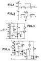
- the circuit according to the invention is shown in its preferred embodiment in FIG. 3.
- the power transistor is designated by the reference Tp.
- the circuit control input is E.
- the entire circuit is supplied between two supply terminals A and B, one of which (B) may consist of an electrical ground and the other (A) of which a positive supply potential Va.
- the transistor Tp authorizes or prohibits the passage of a current in a load L connected between its collector and a positive supply potential which can be the potential Va.
- the emitter of transistor Tp is preferably connected to ground B.
- a conduction circuit For the application of a positive base current, a conduction circuit is provided; for the application of a negative base current, a blocking circuit is provided; these two circuits are connected to the input E which controls them.
- the conduction circuit here comprises the following elements: a transistor T1, PNP, having its emitter connected to terminal A and its collector connected by a resistor R1 to the base of transistor Tp.
- the base of transistor T1 is connected to the midpoint of a divider bridge R2, R3 which is connected between terminals A and E.
- the transistor T1 applies a current or interrupts the current in the base of the transistor Tp.
- the conduction circuit is therefore very simple and could moreover be replaced by other circuit variants such as a simple current source connected between terminal A and the base of Tp, this source being controlled by the terminal.
- a simple current source connected between terminal A and the base of Tp, this source being controlled by the terminal.
- the elements of the circuit are connected in the following manner: the diodes D1 and D2 are in series (and have the same polarity) between the base of the transistor Tp and the terminal B; the junction point of the diodes is connected to an armature of the capacitor C1; the other armature of this capacitor is connected by the resistor R4 to the terminal A and is also connected to the collector of the transistor-switch T2; the emitter of transistor T2 is connected to terminal B; the base of the transistor T2 is connected to a terminal of the capacitor C2 and to a terminal of the resistor R5; the other terminal of resistor R5 is connected to ground B; the other terminal of the capacitor C2 is connected by the resistor R6 to the control input E.
- the circuit operates as follows: for the conduction, the input E is brought to a low potential, which on the one hand makes the transistor T1 conductive and applies a positive base current to the power transistor Tp which is starts driving, and on the other hand discharges the capacitor C2 through the resistors R5 and R6 with a time constant (R5 + R6) C which is brief (of the order of the destocking time of the transistor Tp).
- the discharge time of the capacitor C2 can be reduced to an even lower value by additionally providing a diode or two in parallel on the resistors R5 and R6, the diode being mounted so as to allow the discharge of the charge from the capacity C2 when input E is set to low potential.
- the capacitor C1 charges or more exactly continues to charge if its charge has already started before the conduction signal, which will most often be the case, except perhaps for conduction duty cycles very close to unity.
- the charge of C1 is done through R4 and D1.
- the input E is brought to a high potential. This has the effect of immediately blocking the transistor T1 and therefore of interrupting the positive base current.
- the high potential level is used to immediately bias the transistor T2 in a conductive state, the ratio of the resistors R5 and R6 being chosen such that the voltage applied to the base of the transistor T2 is a sufficient fraction of the potential present between terminals A and E. It is recalled in this connection that the capacitor C2 is initially discharged. Under these conditions, the transistor T2 becomes a quasi-short circuit and establishes a discharge circuit of the capacitor C1.
- the discharge current can only come from the diode D2 and, in the form of negative base current, from the base of the transistor Tp.
- the capacitor C1 While the capacitor C1 thus discharges and allows the flow of the charges stored in the base of the transistor, the capacitor C2 charges through the resistor R6. After a certain time, depending on the charging time constant of the capacitance and the value of the high potential applied to the input E, the base of the transistor T2 no longer receives sufficient current to keep the transistor T2 conducting. It is therefore blocked (gradually) and the basic negative current, after a gradual decrease, is completely interrupted.
- the charging time constant of the capacitor C2 is chosen (through the resistor R6 and the set in parallel of the resistor R5 and of the base-emitter junction of the transistor T2), so that the interruption of the conduction of the transistor T2 and therefore the interruption of the basic negative current takes place after a time which is of the order of magnitude of the time tsou ts + tf (Figure 2); the ideal is to get as close as possible by higher value, to this duration ts + tf, the order of magnitude of which is a few microseconds.
- the capacitor C1 begins to recharge through the resistor R4 and the diode D1.
- capacitor C1 is recharged while the power transistor Tp is blocked; the charge of C1 also continues throughout the rest of the blocking period and also throughout the following conduction period.
- the diode D2 prevents a positive base current from being applied to the base of the transistor Tp as a result of the charge of the capacitor C1 (if a direct connection existed between the capacitor C1 and the base, the charge current of C1 could pass through the base of the transistor Tp and make it conductive while one is in blocking phase ).
- the diode D2 allows by its orientation the passage of this negative current.
- the diode D2 allows, with the help of the diode D1, that a sufficient bias voltage (two direct diode voltage drops) exists between the base and the emitter of the transistor Tp.
- FIG. 4 represents an alternative embodiment in which it is desired that the base of the power transistor be negatively polarized with respect to the emitter during the entire blocking period; this is the case in particular when there are several transistors mounted in a bridge.
- terminal B no longer constitutes a supply terminal but only a node of the circuit.
- the supply terminal is a terminal D and a resistor, two diodes and a capacitor (in the example shown) are added: more precisely, a resistor R7 connects the base to the second supply terminal D; a resistor R8 connects terminal A to node B; two diodes in series D3 and D4 connect node B (anode side) to terminal D (cathode side) and a capacitor C3 is placed in parallel on diodes D3 and D4 between terminals B and D.
- the capacitor C3 charged by the resistor R8 maintains a constant potential difference between terminals B and D, limited by the diodes to a value of approximately 1.3 volts.
- this potential difference is applied to the emitter base junction of the transistor Tp, the base potential then being negative with respect to the emitter potential.
- control circuit of the base of the transistor T2 can be produced differently provided that it performs the function defined above, namely the immediate polarization of the transistor T2 in a conductive state as soon as the signal applied to the input transitions E, then switching off the transistor T2 after a very short time, but sufficient to ensure the destocking of the charges of the power transistor Tp.
Landscapes
- Electronic Switches (AREA)
- Dc-Dc Converters (AREA)
Claims (5)
Applications Claiming Priority (2)
| Application Number | Priority Date | Filing Date | Title |
|---|---|---|---|
| FR8505010 | 1985-04-02 | ||
| FR8505010A FR2579844B1 (fr) | 1985-04-02 | 1985-04-02 | Circuit de commande de base de transistor fonctionnant a frequence elevee |
Publications (2)
| Publication Number | Publication Date |
|---|---|
| EP0200600A1 EP0200600A1 (de) | 1986-11-05 |
| EP0200600B1 true EP0200600B1 (de) | 1990-01-03 |
Family
ID=9317867
Family Applications (1)
| Application Number | Title | Priority Date | Filing Date |
|---|---|---|---|
| EP86400668A Expired - Lifetime EP0200600B1 (de) | 1985-04-02 | 1986-03-27 | Bei hoher Frequenz arbeitende Transistorbasissteuerschaltung |
Country Status (5)
| Country | Link |
|---|---|
| US (1) | US4764686A (de) |
| EP (1) | EP0200600B1 (de) |
| JP (1) | JP2575117B2 (de) |
| DE (1) | DE3668107D1 (de) |
| FR (1) | FR2579844B1 (de) |
Families Citing this family (5)
| Publication number | Priority date | Publication date | Assignee | Title |
|---|---|---|---|---|
| US4728817A (en) * | 1987-02-09 | 1988-03-01 | Westinghouse Electric Corp. | Power transistor drive circuit |
| FR2614153B1 (fr) * | 1987-04-17 | 1994-03-04 | Thomson Csf | Dispositif de commande d'interrupteur a semiconducteur |
| DE3732790A1 (de) * | 1987-09-29 | 1989-04-13 | Thomson Brandt Gmbh | Schaltnetzteil |
| US5036218A (en) * | 1990-03-21 | 1991-07-30 | International Business Machines Corporation | Antisaturation circuit |
| US7295199B2 (en) * | 2003-08-25 | 2007-11-13 | Motorola Inc | Matrix display having addressable display elements and methods |
Family Cites Families (11)
| Publication number | Priority date | Publication date | Assignee | Title |
|---|---|---|---|---|
| US3300072A (en) * | 1965-10-21 | 1967-01-24 | Hoosier Crown Corp | Sealing of crown cap bottles |
| US3569742A (en) * | 1968-08-23 | 1971-03-09 | Gen Precision Systems Inc | Transistor switching circuit |
| US3787738A (en) * | 1972-09-28 | 1974-01-22 | Us Army | Pulse producing circuit |
| US4032834A (en) * | 1972-10-24 | 1977-06-28 | Danfoss A/S | Method for triggering a controlled rectifier and for keeping it conductive and a generator for that purpose |
| JPS51156743U (de) * | 1975-06-09 | 1976-12-14 | ||
| DE2644507C3 (de) * | 1976-10-01 | 1984-07-26 | Siemens AG, 1000 Berlin und 8000 München | Verfahren zur Aussteuerung eines im Sättigungszustand betriebenen Transistors und Vorrichtung zur Durchführung des Verfahrens |
| US4234805A (en) * | 1978-03-15 | 1980-11-18 | Evc, Inc. | Circuit and method for paralleling power transistors |
| JPS5668340U (de) * | 1979-10-30 | 1981-06-06 | ||
| DE3040365A1 (de) * | 1980-10-25 | 1982-05-27 | Licentia Patent-Verwaltungs-Gmbh, 6000 Frankfurt | Steuerschaltung zum schnellen schalten eines steuerbaren halbleiters |
| US4472642A (en) * | 1982-02-12 | 1984-09-18 | Mitsubishi Denki Kabushiki Kaisha | Power semiconductor switching device |
| JPS6028484U (ja) * | 1983-07-29 | 1985-02-26 | 富士電気化学株式会社 | 並列制御式チョッパ−回路 |
-
1985
- 1985-04-02 FR FR8505010A patent/FR2579844B1/fr not_active Expired
-
1986
- 1986-03-27 DE DE8686400668T patent/DE3668107D1/de not_active Expired - Fee Related
- 1986-03-27 EP EP86400668A patent/EP0200600B1/de not_active Expired - Lifetime
- 1986-04-01 JP JP61075403A patent/JP2575117B2/ja not_active Expired - Lifetime
- 1986-04-02 US US06/847,317 patent/US4764686A/en not_active Expired - Lifetime
Also Published As
| Publication number | Publication date |
|---|---|
| JPS61230517A (ja) | 1986-10-14 |
| DE3668107D1 (de) | 1990-02-08 |
| EP0200600A1 (de) | 1986-11-05 |
| FR2579844B1 (fr) | 1987-05-15 |
| JP2575117B2 (ja) | 1997-01-22 |
| US4764686A (en) | 1988-08-16 |
| FR2579844A1 (fr) | 1986-10-03 |
Similar Documents
| Publication | Publication Date | Title |
|---|---|---|
| CA1145815A (fr) | Dispositif de commutation automatique de deux batteries chargees en parallele et dechargees en serie | |
| EP0002983A1 (de) | Leistungssteuerkreis und seine Anwendung in einer pulsierenden Spannungsspeiseeinrichtung | |
| FR2782204A1 (fr) | Circuit pour eliminer l'energie magnetique stockee dans un enroulement d'excitation d'un generateur | |
| EP0329571B1 (de) | Schaltungsanordnung zur Überwachung der Entmagnetisierung für einen Sperrwandler mit primärseitiger und secundärseitiger Regelung | |
| EP0200600B1 (de) | Bei hoher Frequenz arbeitende Transistorbasissteuerschaltung | |
| EP0820141A2 (de) | Nullspannungsansteuerung einer hybriden Brückenschaltung | |
| EP1528661B1 (de) | Steuerschaltung für einen MOS-Transistor für Synchrongleichrichter | |
| EP0562908A1 (de) | Speiseschaltung für ein elektrisches Relais | |
| EP1061650A1 (de) | Bistabiler Zweirichtungs-Hochspannungsschalter | |
| EP0265322B1 (de) | Standby-Betriebssteuerschaltung für ein Schaltnetzteil | |
| EP0654885B1 (de) | Stromversorgungsvorrichtung für die Steuerschaltung eines Leistungsschalters | |
| EP0370896B1 (de) | Leistungs-Schalteinrichtung, insbesondere für Umrichter | |
| EP1320919B1 (de) | Dauerbetriebsbegrenzung in einem schaltnetzteil | |
| EP0331592A1 (de) | Schaltnetzteil mit progressivem Start | |
| EP0955718A1 (de) | Schaltspannungswandler | |
| EP1227590B1 (de) | Verfahren und Vorrichtung zum Aufbereiten von einer zum Betrieb eines elektronischen Schalters nötigen Versorgungsspannung | |
| CH682019A5 (en) | Amplitude control circuit for oscillator circuit - includes current sources and current mirror in circuit to limit final output voltage of oscillator control circuit | |
| EP1493522A1 (de) | Drahtfunkenerosionsmaschine | |
| EP0196934B1 (de) | Steuerschaltung für Taktversorgung für verschiedene Anwendungen | |
| EP0031626B1 (de) | Steuervorrichtung für die Triggerelektrode eines Halbleiterschalters eines bidirektionalen Systems | |
| FR2751805A1 (fr) | Convertisseur abaisseur a demagnetisation complete auto-oscillant | |
| EP0132173B1 (de) | Schaltungsanordnung für Fernsprecher zur zeitlich definierten Leitungsunterbrechung | |
| EP0554154B1 (de) | Verwaltungsschaltung für Erregerstromsteuervorrichtung | |
| EP0270450B1 (de) | Niederspannungsversorgungsschaltung ohne Netzspannungsabwärtstransformator | |
| FR2665322A1 (fr) | Convertisseur pour alimentation de lampes. |
Legal Events
| Date | Code | Title | Description |
|---|---|---|---|
| PUAI | Public reference made under article 153(3) epc to a published international application that has entered the european phase |
Free format text: ORIGINAL CODE: 0009012 |
|
| AK | Designated contracting states |
Kind code of ref document: A1 Designated state(s): DE FR GB IT NL |
|
| PUAB | Information related to the publication of an a document modified or deleted |
Free format text: ORIGINAL CODE: 0009199EPPU |
|
| PUAF | Information related to the publication of a search report (a3 document) modified or deleted |
Free format text: ORIGINAL CODE: 0009199SEPU |
|
| 17P | Request for examination filed |
Effective date: 19861120 |
|
| R17D | Deferred search report published (corrected) |
Effective date: 19861210 |
|
| RA1 | Application published (corrected) |
Date of ref document: 19861210 Kind code of ref document: A1 |
|
| 17Q | First examination report despatched |
Effective date: 19890120 |
|
| RAP3 | Party data changed (applicant data changed or rights of an application transferred) |
Owner name: THOMSON-CSF |
|
| GRAA | (expected) grant |
Free format text: ORIGINAL CODE: 0009210 |
|
| AK | Designated contracting states |
Kind code of ref document: B1 Designated state(s): DE FR GB IT NL |
|
| PG25 | Lapsed in a contracting state [announced via postgrant information from national office to epo] |
Ref country code: NL Effective date: 19900103 |
|
| ITF | It: translation for a ep patent filed | ||
| REF | Corresponds to: |
Ref document number: 3668107 Country of ref document: DE Date of ref document: 19900208 |
|
| GBT | Gb: translation of ep patent filed (gb section 77(6)(a)/1977) | ||
| NLV1 | Nl: lapsed or annulled due to failure to fulfill the requirements of art. 29p and 29m of the patents act | ||
| PLBE | No opposition filed within time limit |
Free format text: ORIGINAL CODE: 0009261 |
|
| STAA | Information on the status of an ep patent application or granted ep patent |
Free format text: STATUS: NO OPPOSITION FILED WITHIN TIME LIMIT |
|
| 26N | No opposition filed | ||
| ITTA | It: last paid annual fee | ||
| REG | Reference to a national code |
Ref country code: FR Ref legal event code: D6 |
|
| PGFP | Annual fee paid to national office [announced via postgrant information from national office to epo] |
Ref country code: FR Payment date: 20010313 Year of fee payment: 16 |
|
| PGFP | Annual fee paid to national office [announced via postgrant information from national office to epo] |
Ref country code: DE Payment date: 20010319 Year of fee payment: 16 |
|
| PGFP | Annual fee paid to national office [announced via postgrant information from national office to epo] |
Ref country code: GB Payment date: 20010321 Year of fee payment: 16 |
|
| REG | Reference to a national code |
Ref country code: GB Ref legal event code: IF02 |
|
| PG25 | Lapsed in a contracting state [announced via postgrant information from national office to epo] |
Ref country code: GB Free format text: LAPSE BECAUSE OF NON-PAYMENT OF DUE FEES Effective date: 20020327 |
|
| PG25 | Lapsed in a contracting state [announced via postgrant information from national office to epo] |
Ref country code: DE Free format text: LAPSE BECAUSE OF NON-PAYMENT OF DUE FEES Effective date: 20021001 |
|
| GBPC | Gb: european patent ceased through non-payment of renewal fee |
Effective date: 20020327 |
|
| PG25 | Lapsed in a contracting state [announced via postgrant information from national office to epo] |
Ref country code: FR Free format text: LAPSE BECAUSE OF NON-PAYMENT OF DUE FEES Effective date: 20021129 |
|
| REG | Reference to a national code |
Ref country code: FR Ref legal event code: ST |
|
| PG25 | Lapsed in a contracting state [announced via postgrant information from national office to epo] |
Ref country code: IT Free format text: LAPSE BECAUSE OF NON-PAYMENT OF DUE FEES;WARNING: LAPSES OF ITALIAN PATENTS WITH EFFECTIVE DATE BEFORE 2007 MAY HAVE OCCURRED AT ANY TIME BEFORE 2007. THE CORRECT EFFECTIVE DATE MAY BE DIFFERENT FROM THE ONE RECORDED. Effective date: 20050327 |