EP0200600B1 - Transistor base control circuit operating at a high frequency - Google Patents
Transistor base control circuit operating at a high frequency Download PDFInfo
- Publication number
- EP0200600B1 EP0200600B1 EP86400668A EP86400668A EP0200600B1 EP 0200600 B1 EP0200600 B1 EP 0200600B1 EP 86400668 A EP86400668 A EP 86400668A EP 86400668 A EP86400668 A EP 86400668A EP 0200600 B1 EP0200600 B1 EP 0200600B1
- Authority
- EP
- European Patent Office
- Prior art keywords
- circuit
- capacitor
- switch
- power transistor
- transistor
- Prior art date
- Legal status (The legal status is an assumption and is not a legal conclusion. Google has not performed a legal analysis and makes no representation as to the accuracy of the status listed.)
- Expired - Lifetime
Links
Images
Classifications
-
- H—ELECTRICITY
- H03—ELECTRONIC CIRCUITRY
- H03K—PULSE TECHNIQUE
- H03K17/00—Electronic switching or gating, i.e. not by contact-making and –breaking
- H03K17/04—Modifications for accelerating switching
- H03K17/041—Modifications for accelerating switching without feedback from the output circuit to the control circuit
- H03K17/0412—Modifications for accelerating switching without feedback from the output circuit to the control circuit by measures taken in the control circuit
- H03K17/04126—Modifications for accelerating switching without feedback from the output circuit to the control circuit by measures taken in the control circuit in bipolar transistor switches
Definitions
- the present invention relates to the switching control of power transistors at high frequencies, for example in the range of 10 to 100 kilohertz.
- the base current Ib of the transistor has the shape shown in Figure 2. As shown in Figure 2 , the base current Ib must be of a first polarity when the transistor must be conductive.
- the current which makes the transistor conductive will hereinafter be called by positive base current convention; this convention corresponds to a current entering the base for an NPN power transistor.
- this minimum value becomes a very large fraction of the switching period and the circuit can no longer be operated with a low conduction duty cycle, i.e. say with a weak relationship between the conduction time and the switching period.
- the present invention provides a new conduction and blocking control circuit for a power transistor which, while being very simple and while using only a small number of components, eliminates this drawback.
- the circuit according to the invention as claimed comprises, as in the known technique, a control input connected to a conduction circuit and to a blocking circuit, the conduction circuit supplying the power transistor with a positive base current. or zero according to the state of the control input, and the blocking circuit first supplying a negative initial base current when receiving a blocking order on the control input then a zero base current .
- the capacitor has a first armature connected on the one hand to a charging means and on the other hand to the emitter-collector circuit of a transistor-switch, and a second armature connected to a first diode oriented in one direction allowing the capacitor to charge by the charging means during the whole time that the switch transistor is blocked.
- a second diode is connected between the base of the power transistor and the second armature of the capacitor and is oriented in a direction allowing the passage of a negative base current through a discharge circuit constituted by the base of the power transistor, the second diode, the capacitor, and the transistor-switch (when the latter is made conductive); finally, the circuit for temporarily closing the switch comprises a series assembly of at least one resistor and one capacitor, this assembly constituting a series RC network connected to the control input so that the capacitor can receive a load current when the input receives a blocking control signal from the power transistor; the RC series assembly is also connected to a control terminal of the transistor-switch, for on the one hand instantly transmitting a conduction signal of the transistor-switch, upon reception of a blocking control signal from the power transistor, on the other hand to start at the same time the application of a load current to the capacitance of the re RC bucket, and finally to interrupt the conduction of the switch transistor after a time determined by the charge time constant of the capacity
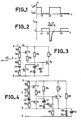
- the circuit according to the invention is shown in its preferred embodiment in FIG. 3.
- the power transistor is designated by the reference Tp.
- the circuit control input is E.
- the entire circuit is supplied between two supply terminals A and B, one of which (B) may consist of an electrical ground and the other (A) of which a positive supply potential Va.
- the transistor Tp authorizes or prohibits the passage of a current in a load L connected between its collector and a positive supply potential which can be the potential Va.
- the emitter of transistor Tp is preferably connected to ground B.
- a conduction circuit For the application of a positive base current, a conduction circuit is provided; for the application of a negative base current, a blocking circuit is provided; these two circuits are connected to the input E which controls them.
- the conduction circuit here comprises the following elements: a transistor T1, PNP, having its emitter connected to terminal A and its collector connected by a resistor R1 to the base of transistor Tp.
- the base of transistor T1 is connected to the midpoint of a divider bridge R2, R3 which is connected between terminals A and E.
- the transistor T1 applies a current or interrupts the current in the base of the transistor Tp.
- the conduction circuit is therefore very simple and could moreover be replaced by other circuit variants such as a simple current source connected between terminal A and the base of Tp, this source being controlled by the terminal.
- a simple current source connected between terminal A and the base of Tp, this source being controlled by the terminal.
- the elements of the circuit are connected in the following manner: the diodes D1 and D2 are in series (and have the same polarity) between the base of the transistor Tp and the terminal B; the junction point of the diodes is connected to an armature of the capacitor C1; the other armature of this capacitor is connected by the resistor R4 to the terminal A and is also connected to the collector of the transistor-switch T2; the emitter of transistor T2 is connected to terminal B; the base of the transistor T2 is connected to a terminal of the capacitor C2 and to a terminal of the resistor R5; the other terminal of resistor R5 is connected to ground B; the other terminal of the capacitor C2 is connected by the resistor R6 to the control input E.
- the circuit operates as follows: for the conduction, the input E is brought to a low potential, which on the one hand makes the transistor T1 conductive and applies a positive base current to the power transistor Tp which is starts driving, and on the other hand discharges the capacitor C2 through the resistors R5 and R6 with a time constant (R5 + R6) C which is brief (of the order of the destocking time of the transistor Tp).
- the discharge time of the capacitor C2 can be reduced to an even lower value by additionally providing a diode or two in parallel on the resistors R5 and R6, the diode being mounted so as to allow the discharge of the charge from the capacity C2 when input E is set to low potential.
- the capacitor C1 charges or more exactly continues to charge if its charge has already started before the conduction signal, which will most often be the case, except perhaps for conduction duty cycles very close to unity.
- the charge of C1 is done through R4 and D1.
- the input E is brought to a high potential. This has the effect of immediately blocking the transistor T1 and therefore of interrupting the positive base current.
- the high potential level is used to immediately bias the transistor T2 in a conductive state, the ratio of the resistors R5 and R6 being chosen such that the voltage applied to the base of the transistor T2 is a sufficient fraction of the potential present between terminals A and E. It is recalled in this connection that the capacitor C2 is initially discharged. Under these conditions, the transistor T2 becomes a quasi-short circuit and establishes a discharge circuit of the capacitor C1.
- the discharge current can only come from the diode D2 and, in the form of negative base current, from the base of the transistor Tp.
- the capacitor C1 While the capacitor C1 thus discharges and allows the flow of the charges stored in the base of the transistor, the capacitor C2 charges through the resistor R6. After a certain time, depending on the charging time constant of the capacitance and the value of the high potential applied to the input E, the base of the transistor T2 no longer receives sufficient current to keep the transistor T2 conducting. It is therefore blocked (gradually) and the basic negative current, after a gradual decrease, is completely interrupted.
- the charging time constant of the capacitor C2 is chosen (through the resistor R6 and the set in parallel of the resistor R5 and of the base-emitter junction of the transistor T2), so that the interruption of the conduction of the transistor T2 and therefore the interruption of the basic negative current takes place after a time which is of the order of magnitude of the time tsou ts + tf (Figure 2); the ideal is to get as close as possible by higher value, to this duration ts + tf, the order of magnitude of which is a few microseconds.
- the capacitor C1 begins to recharge through the resistor R4 and the diode D1.
- capacitor C1 is recharged while the power transistor Tp is blocked; the charge of C1 also continues throughout the rest of the blocking period and also throughout the following conduction period.
- the diode D2 prevents a positive base current from being applied to the base of the transistor Tp as a result of the charge of the capacitor C1 (if a direct connection existed between the capacitor C1 and the base, the charge current of C1 could pass through the base of the transistor Tp and make it conductive while one is in blocking phase ).
- the diode D2 allows by its orientation the passage of this negative current.
- the diode D2 allows, with the help of the diode D1, that a sufficient bias voltage (two direct diode voltage drops) exists between the base and the emitter of the transistor Tp.
- FIG. 4 represents an alternative embodiment in which it is desired that the base of the power transistor be negatively polarized with respect to the emitter during the entire blocking period; this is the case in particular when there are several transistors mounted in a bridge.
- terminal B no longer constitutes a supply terminal but only a node of the circuit.
- the supply terminal is a terminal D and a resistor, two diodes and a capacitor (in the example shown) are added: more precisely, a resistor R7 connects the base to the second supply terminal D; a resistor R8 connects terminal A to node B; two diodes in series D3 and D4 connect node B (anode side) to terminal D (cathode side) and a capacitor C3 is placed in parallel on diodes D3 and D4 between terminals B and D.
- the capacitor C3 charged by the resistor R8 maintains a constant potential difference between terminals B and D, limited by the diodes to a value of approximately 1.3 volts.
- this potential difference is applied to the emitter base junction of the transistor Tp, the base potential then being negative with respect to the emitter potential.
- control circuit of the base of the transistor T2 can be produced differently provided that it performs the function defined above, namely the immediate polarization of the transistor T2 in a conductive state as soon as the signal applied to the input transitions E, then switching off the transistor T2 after a very short time, but sufficient to ensure the destocking of the charges of the power transistor Tp.
Description
La présente invention concerne la commande en commutation des transistors de puissance à des fréquences élevées, par exemple dans la gamme de 10 à 100 kilohertz.The present invention relates to the switching control of power transistors at high frequencies, for example in the range of 10 to 100 kilohertz.
Etant donné un signal d'ordre de commutation S (figure 1) susceptible de passer d'un premier état ou état "off", dans lequel le transistor de puissance est bloqué, à un deuxième état ou état "on" dans lequel le transistor de puissance est conducteur, il est connu que, si l'on souhaite une commutation rapide d'un état à l'autre, le courant de base Ib du transistor ait l'allure représentée à la figure 2. Comme le montre la figure 2, le courant de base Ib doit être d'une première polarité lorsque le transistor doit être conducteur. On appellera ci-après par convention courant de base positif le courant qui rend le transistor conducteur; cette convention correspond à un courant entrant dans la base pour un transistor de puissance NPN. A l'instant où le signal S passe de l'état "on" à l'état "off", il ne suffit pas de mettre à zéro le courant de base Ib mais il faut initialement extraire de la base un courant de polarité inverse (qu'on appellera courant de base négatif par convention). Ce courant négatif est absolument nécessaire si on veut assurer une commutation rapide du transistor de l'état conducteur vers l'état bloqué. En effet, seul ce courant de base négatif permet d'éliminer assez rapidement les charges électriques qui se sont accumulées dans la base du transistor pendant la période de conduction. Le courant de base négatif est sensiblement constant pendant une durée ts suivant l'ordre de blocage (temps de déstockage) puis il revient à zéro pendant une durée tf (temps de descente).Given a switching order signal S (FIG. 1) capable of passing from a first state or state "off", in which the power transistor is blocked, to a second state or state "on" in which the transistor power is conductive, it is known that, if you want rapid switching from one state to another, the base current Ib of the transistor has the shape shown in Figure 2. As shown in Figure 2 , the base current Ib must be of a first polarity when the transistor must be conductive. The current which makes the transistor conductive will hereinafter be called by positive base current convention; this convention corresponds to a current entering the base for an NPN power transistor. At the moment when the signal S goes from the "on" state to the "off" state, it is not enough to zero the base current Ib but it is initially necessary to extract from the base a current of reverse polarity (which will be called negative base current by convention). This negative current is absolutely necessary if we want to ensure rapid switching of the transistor from the conducting state to the blocked state. Indeed, only this negative base current makes it possible to eliminate fairly quickly the electric charges which have accumulated in the base of the transistor during the conduction period. The negative base current is substantially constant during a period ts according to the blocking order (destocking time) then it returns to zero during a period tf (descent time).
A priori, pour donner au courant de base cette allure générale, il faut disposer de deux sources d'alimentation de polarités opposées. Ceci constitue un inconvénient évident, et on a donc cherché à réaliser des circuits capables de fournir le courant de base négatif sans source d'alimentation négative. Pour cela, on utilise en général un condensateur ou une inductance qui stocke de l'énergie pendant la période de conduction du transistor et la restitue sous forme de courant de base négatif au moment où on déclenche l'ordre de blocage du transistor.A priori, to give the basic current this general appearance, it is necessary to have two power sources of opposite polarities. This constitutes an obvious drawback, and we have therefore sought to produce circuits capable of supplying the negative base current without a negative power source. For that, one generally uses a capacitor or an inductance which stores energy during the conduction period of the transistor and restores it in the form of negative base current at the moment when the blocking order of the transistor is triggered.
Toutefois la plupart des circuits réalisés jusqu'à maintenant dont le circuit connu du document DE-A 3 040 365 est un exemple souffrent d'un inconvénient important: pour que le circuit fonctionne convenablement, il faut que le condensateur ou l'inductance ait le temps de stocker suffisamment d'énergie pendant la durée de conduction. Cela impose que la durée de conduction ait une valeur minimale qui ne soit pas trop faible.However, most of the circuits produced up to now, of which the circuit known from document DE-A 3 040 365 is an example, suffer from an important drawback: for the circuit to function properly, the capacitor or the inductor must have the time to store enough energy during the conduction time. This requires that the conduction time has a minimum value which is not too low.
Si la période de commutation est faible (travail à haute fréquence), cette valeur minimale devient une fraction très importante de la période de commutation et on ne peut plus faire fonctionner le circuit avec un faible rapport cyclique de conduction, c'est-à-dire avec un faible rapport entre la durée de conduction et la période de commutation.If the switching period is low (high frequency work), this minimum value becomes a very large fraction of the switching period and the circuit can no longer be operated with a low conduction duty cycle, i.e. say with a weak relationship between the conduction time and the switching period.
La présente invention propose un nouveau circuit de commande de conduction et blocage d'un transistor de puissance qui, tout étant très simple et tout en n'utilisant qu'un faible nombre de composants, élimine cet inconvénient.The present invention provides a new conduction and blocking control circuit for a power transistor which, while being very simple and while using only a small number of components, eliminates this drawback.
Le circuit selon l'invention telle que revendiquée comprend comme dans la technique connue une entrée de commande reliée à un circuit de mise en conduction et à un circuit de blocage, le circuit de mise en conduction fournissant au transistor de puissance un courant de base positif ou nul selon l'état de l'entrée de commande, et le circuit de blocage fournissant d'abord un courant de base initial négatif lors de la réception d'un ordre de blocage sur l'entrée de commande puis un courant de base nul.The circuit according to the invention as claimed comprises, as in the known technique, a control input connected to a conduction circuit and to a blocking circuit, the conduction circuit supplying the power transistor with a positive base current. or zero according to the state of the control input, and the blocking circuit first supplying a negative initial base current when receiving a blocking order on the control input then a zero base current .
De plus, selon l'invention telle que revendiquée, le circuit de blocage comprend les éléments suivants :
- - un condensateur pour stocker de l'énergie nécessaire à la production d'un courant négatif de base ;
- - un moyen pour charger le condensateur pendant la période de conduction et pendant la période de blocage du transistor de puissance ;
- - un interrupteur commandé pour établir un circuit de décharge du condensateur dans la base du transistor de puissance, le courant circulant dans ce circuit de décharge lors de la fermeture de l'interrupteur correspondant à un courant de base négatif ;
- - un circuit de commande de fermeture temporaire de l'interrupteur, ce circuit commandant la fermeture de l'interrupteur dès la réception d'un ordre de blocage sur l'entrée de commande et pendant une courte durée prédéterminée qui est de l'ordre de grandeur du temps de déstockage du transistor de puissance.
- - a capacitor for storing energy necessary for the production of a negative base current;
- a means for charging the capacitor during the conduction period and during the blocking period of the power transistor;
- - a controlled switch to establish a discharge circuit of the capacitor in the base of the power transistor, the current flowing in this discharge circuit when the switch closes corresponding to a negative base current;
- a circuit for controlling the temporary closing of the switch, this circuit controlling the closing of the switch as soon as a blocking order is received on the control input and for a short predetermined duration which is of the order of magnitude of the power transistor destocking time.
Dans un mode de réalisation préférentiel de l'invention, le condensateur a une première armature reliée d'une part à un moyen de charge et d'autre part au circuit émetteur-collecteur d'un transistor-interrupteur, et une deuxième armature reliée à une première diode orientée dans un sens permettant au condensateur de se charger par le moyen de charge pendant tout le temps que le transistor interrupteur est bloqué. Une deuxième diode est reliée entre la base du transistor de puissance et la deuxième armature du condensateur et est orientée dans un sens permettant le passage d'un courant de base négatif à travers un circuit de décharge constitué par la base du transistor de puissance, la deuxième diode, le condensateur, et le transistor-interrupteur (lorsque celui-ci est rendu conducteur); enfin, le circuit de commande de fermeture temporaire de l'interrupteur comprend un ensemble en série d'au moins une résistance et une capacité, cet ensemble constituant un réseau RC série relié à l'entrée de commande de manière que la capacité puisse recevoir un courant de charge lorsque l'entrée reçoit un signal de commande de blocage du transistor de puissance; l'ensemble RC série est par ailleurs connecté à une borne de commande du transistor-interrupteur, pour d'une part transmettre instantanément un signal de mise en conduction du transistor-interrupteur, lors de la réception d'un signal de commande de blocage du transistor de puissance, d'autre part pour commencer au même moment l'application d'un courant de charge à la capacité du réseau RC, et enfin pour interrompre la mise en conduction du transistor interrupteur au bout d'un temps déterminé par la constante de temps de charge de la capacité du réseau RC, ce temps étant de l'ordre du temps de déstockage des charges du transistor de puissance.In a preferred embodiment of the invention, the capacitor has a first armature connected on the one hand to a charging means and on the other hand to the emitter-collector circuit of a transistor-switch, and a second armature connected to a first diode oriented in one direction allowing the capacitor to charge by the charging means during the whole time that the switch transistor is blocked. A second diode is connected between the base of the power transistor and the second armature of the capacitor and is oriented in a direction allowing the passage of a negative base current through a discharge circuit constituted by the base of the power transistor, the second diode, the capacitor, and the transistor-switch (when the latter is made conductive); finally, the circuit for temporarily closing the switch comprises a series assembly of at least one resistor and one capacitor, this assembly constituting a series RC network connected to the control input so that the capacitor can receive a load current when the input receives a blocking control signal from the power transistor; the RC series assembly is also connected to a control terminal of the transistor-switch, for on the one hand instantly transmitting a conduction signal of the transistor-switch, upon reception of a blocking control signal from the power transistor, on the other hand to start at the same time the application of a load current to the capacitance of the re RC bucket, and finally to interrupt the conduction of the switch transistor after a time determined by the charge time constant of the capacity of the RC network, this time being of the order of the destocking time of the charges of the transistor power.
D'autres caractéristiques et avantages de l'invention apparaîtront à la lecture de la description détaillée qui suit et qui est faite en référence aux dessins annexés dans lesquels :
- - les figures 1 et 2 déjà décrites représentent des diagrammes temporels du signal de commande appliqué à l'entrée d'un circuit de commande de transistor de puissance et le courant de base qui doit en résulter ;
- - la figure 3 représente un mode de réalisation préférentiel de l'invention ;
- - la figure 4 représente une variante de réalisation.
- - Figures 1 and 2 already described represent time diagrams of the control signal applied to the input of a power transistor control circuit and the base current which must result therefrom;
- - Figure 3 shows a preferred embodiment of the invention;
- - Figure 4 shows an alternative embodiment.
Le circuit selon l'invention est représenté dans sa réalisation préférentielle à la figure 3.The circuit according to the invention is shown in its preferred embodiment in FIG. 3.
Le transistor de puissance est désigné par la référence Tp. L'entrée de commande du circuit est E. L'ensemble du circuit est alimenté entre deux bornes d'alimentation A et B dont l'une (B) peut être constituée par une masse électrique et l'autre (A) est portée à un potentiel d'alimentation positif Va.The power transistor is designated by the reference Tp. The circuit control input is E. The entire circuit is supplied between two supply terminals A and B, one of which (B) may consist of an electrical ground and the other (A) of which a positive supply potential Va.
Le transistor Tp autorise ou interdit le passage d'un courant dans une charge L reliée entre son collecteur et un potentiel d'alimentation positif qui peut être le potentiel Va. L'émetteur du transistor Tp est de préférence relié à la masse B.The transistor Tp authorizes or prohibits the passage of a current in a load L connected between its collector and a positive supply potential which can be the potential Va. The emitter of transistor Tp is preferably connected to ground B.
Pour l'application d'un courant de base positif, un circuit de mise en conduction est prévu; pour l'application d'un courant de base négatif, un circuit de blocage est prévu ; ces deux circuits sont reliés à l'entrée E qui les commande.For the application of a positive base current, a conduction circuit is provided; for the application of a negative base current, a blocking circuit is provided; these two circuits are connected to the input E which controls them.
Le circuit de mise en conduction comprend ici les éléments suivants : un transistor T1, PNP, ayant son émetteur relié à la borne A et son collecteur relié par une résistance R1 à la base du transistor Tp. La base du transistor T1 est reliée au point milieu d'un pont diviseur R2, R3 qui est connecté entre les bornes A et E. Selon que le niveau de tension sur l'entrée E est bas (commande de mise en conduction du transistor Tp) ou haut (commande de blocage), le transistor T1 applique un courant ou interrompt le courant dans la base du transistor Tp.The conduction circuit here comprises the following elements: a transistor T1, PNP, having its emitter connected to terminal A and its collector connected by a resistor R1 to the base of transistor Tp. The base of transistor T1 is connected to the midpoint of a divider bridge R2, R3 which is connected between terminals A and E. Depending on whether the voltage level on input E is low (command to turn on transistor Tp ) or high (blocking command), the transistor T1 applies a current or interrupts the current in the base of the transistor Tp.
Le circuit de mise en conduction est donc très simple et pourrait d'ailleurs être remplacé par d'autres variantes de circuit telles qu'une simple source de courant connectée entre la borne A et la base de Tp, cette source étant commandée par la borne E.The conduction circuit is therefore very simple and could moreover be replaced by other circuit variants such as a simple current source connected between terminal A and the base of Tp, this source being controlled by the terminal. E.
Le circuit de commande de blocage comprend les autres éléments de la figure 3, c'est-à-dire :
- - un condensateur C1 qui sert à stocker l'énergie nécessaire à la production d'un courant de base négatif pour assurer le déstockage des charges au début du blocage du transistor Tp ;
- - une résistance R4 et une diode D1 qui servent à charger le condensateur C1,
- - un interrupteur constitué ici par un transistor T2, NPN ; cet interrupteur établit, lorsqu'il se ferme, un circuit de décharge du condensateur C1,
- - un circuit de commande de l'interrupteur, comprenant deux résistances R5, R6 et une capacité C2 ;
- - et enfin une diode D2 reliée entre la base et le condensateur C1 et ayant plusieurs fonctions indiquées plus loin.
- - a capacitor C1 which is used to store the energy necessary for the production of a negative base current to ensure the destocking of the charges at the start of the blocking of the transistor Tp;
- - a resistor R4 and a diode D1 which are used to charge the capacitor C1,
- - a switch constituted here by a transistor T2, NPN; this switch establishes, when it closes, a discharge circuit of the capacitor C1,
- - a switch control circuit, comprising two resistors R5, R6 and a capacitor C2;
- - And finally a diode D2 connected between the base and the capacitor C1 and having several functions indicated below.
Plus précisément, les éléments du circuit sont connectés de la manière suivant : les diodes D1 et D2 sont en série (et ont la même polarité) entre la base du transistor Tp et la borne B ; le point de jonction des diodes est relié à une armature du condensateur C1 ; l'autre armature de ce condensateur est reliée par la résistance R4 à la borne A et est reliée par ailleurs au collecteur du transistor-interrupteur T2 ; l'émetteur du transistor T2 est relié à la borne B ; la base du transistor T2 est reliée à une borne de la capacité C2 et à une borne de la résistance R5; l'autre borne de la résistance R5 est reliée à la masse B; l'autre borne de la capacité C2 est reliée par la résistance R6 à l'entrée de commande E.More precisely, the elements of the circuit are connected in the following manner: the diodes D1 and D2 are in series (and have the same polarity) between the base of the transistor Tp and the terminal B; the junction point of the diodes is connected to an armature of the capacitor C1; the other armature of this capacitor is connected by the resistor R4 to the terminal A and is also connected to the collector of the transistor-switch T2; the emitter of transistor T2 is connected to terminal B; the base of the transistor T2 is connected to a terminal of the capacitor C2 and to a terminal of the resistor R5; the other terminal of resistor R5 is connected to ground B; the other terminal of the capacitor C2 is connected by the resistor R6 to the control input E.
Le circuit fonctionne de la manière suivante : pour la mise en conduction, l'entrée E est portée à un potentiel bas, ce qui d'une part rend conducteur le transistor T1 et applique un courant de base positif au transistor de puissance Tp qui se met à conduire, et d'autre part décharge la capacité C2 à travers les résistances R5 et R6 avec une constante de temps (R5 + R6) C qui est brève (de l'ordre du temps de déstockage du transistor Tp). On peut réduire à une valeur encore plus faible la durée de décharge de la capacité C2 en prévoyant en outre une diode ou deux en parallèle sur les résistances R5 et R6, la diode étant montée de manière à permettre l'évacuation de la charge de la capacité C2 lorsque l'entrée E est mise au potentiel bas. Pendant ce temps le condensateur C1 se charge ou plus exactement continue à se charger si sa charge a déjà commencé avant le signal de mise en conduction, ce qui sera le plus souvent le cas, sauf peut être pour des rapports cycliques de conduction très proches de l'unité. La charge de C1 se fait à travers R4 et D1.The circuit operates as follows: for the conduction, the input E is brought to a low potential, which on the one hand makes the transistor T1 conductive and applies a positive base current to the power transistor Tp which is starts driving, and on the other hand discharges the capacitor C2 through the resistors R5 and R6 with a time constant (R5 + R6) C which is brief (of the order of the destocking time of the transistor Tp). The discharge time of the capacitor C2 can be reduced to an even lower value by additionally providing a diode or two in parallel on the resistors R5 and R6, the diode being mounted so as to allow the discharge of the charge from the capacity C2 when input E is set to low potential. During this time the capacitor C1 charges or more exactly continues to charge if its charge has already started before the conduction signal, which will most often be the case, except perhaps for conduction duty cycles very close to unity. The charge of C1 is done through R4 and D1.
Pour le blocage du transistor Tp, l'entrée E est portée à un potentiel haut. Ceci a pour effet de bloquer immédiatement le transistor T1 et donc d'interrompre le courant de base positif. D'autre part, le niveau de potentiel haut sert à polariser immédiatement le transistor T2 dans un état conducteur, le rapport des résistances R5 et R6 étant choisi tel que la tension appliquée à la base du transistor T2 soit une fraction suffisante du potentiel présent entre les bornes A et E. On rappelle à ce propos que le condensateur C2 est initialement déchargé. Dans ces conditions, le transistor T2 devient un quasi court-circuit et établit un circuit de décharge du condensateur C1. Comme le transistor T1 est bloqué et comme la diode D1 est orientée dans un sens permettant la charge mais non la décharge du condensateur C1, le courant de décharge ne peut provenir que de la diode D2 et, sous forme de courant de base négatif, de la base du transistor Tp.For blocking the transistor Tp, the input E is brought to a high potential. This has the effect of immediately blocking the transistor T1 and therefore of interrupting the positive base current. On the other hand, the high potential level is used to immediately bias the transistor T2 in a conductive state, the ratio of the resistors R5 and R6 being chosen such that the voltage applied to the base of the transistor T2 is a sufficient fraction of the potential present between terminals A and E. It is recalled in this connection that the capacitor C2 is initially discharged. Under these conditions, the transistor T2 becomes a quasi-short circuit and establishes a discharge circuit of the capacitor C1. As the transistor T1 is blocked and as the diode D1 is oriented in a direction allowing the charge but not the discharge of the capacitor C1, the discharge current can only come from the diode D2 and, in the form of negative base current, from the base of the transistor Tp.
Pendant que le condensateur C1 se décharge ainsi et permet l'écoulement des charges stockées dans la base du transistor, la capacité C2 se charge à travers la résistance R6. Au bout d'un certain temps, dépendant de la constante de temps de charge de la capacité et de la valeur du potentiel haut appliqué à l'entrée E, la base du transistor T2 ne reçoit plus un courant suffisant pour maintenir le transistor T2 conducteur. Celui-ci se bloque donc (progressivement) et le courant négatif de base, après une diminution progressive, s'interrompt totalement.While the capacitor C1 thus discharges and allows the flow of the charges stored in the base of the transistor, the capacitor C2 charges through the resistor R6. After a certain time, depending on the charging time constant of the capacitance and the value of the high potential applied to the input E, the base of the transistor T2 no longer receives sufficient current to keep the transistor T2 conducting. It is therefore blocked (gradually) and the basic negative current, after a gradual decrease, is completely interrupted.
On choisit la constante de temps de charge de la capacité C2 (à travers la résistance R6 et l'ensemble en parallèle de la résistance R5 et de la jonction base-émetteur du transistor T2), pour que l'interruption de la conduction du transistor T2 et donc l'interruption du courant négatif de base ait lieu au bout d'un temps qui est de l'ordre de grandeur du temps tsou ts + tf (figure 2) ; l'idéal est de se rapprocher le plus possible par valeur supérieure, de cette durée ts + tf, dont l'ordre de grandeur est de quelques microsecondes.The charging time constant of the capacitor C2 is chosen (through the resistor R6 and the set in parallel of the resistor R5 and of the base-emitter junction of the transistor T2), so that the interruption of the conduction of the transistor T2 and therefore the interruption of the basic negative current takes place after a time which is of the order of magnitude of the time tsou ts + tf (Figure 2); the ideal is to get as close as possible by higher value, to this duration ts + tf, the order of magnitude of which is a few microseconds.
Par sécurité on choisira une constante de temps sensiblement supérieure à ts + tf pour un transistor donné supposé commuter dans des conditions normales ; une valeur 2(ts + tf) parait raisonnable.For security, we will choose a time constant substantially greater than ts + tf for a given transistor assumed to switch under normal conditions; a value of 2 (ts + tf) seems reasonable.
Dès que le transistor T2 est bloqué, c'est-à-dire au bout d'un temps très court devant la période de commutation, le condensateur C1 commence à se recharger à travers la résistance R4 et la diode D1.As soon as the transistor T2 is blocked, that is to say after a very short time before the switching period, the capacitor C1 begins to recharge through the resistor R4 and the diode D1.
Il est important de constater que le condensateur C1 se recharge alors que le transistor de puissance Tp est bloqué; la charge de C1 se poursuit d'ailleurs pendant toute la suite de la durée de blocage et également pendant toute la durée de conduction qui suit.It is important to note that the capacitor C1 is recharged while the power transistor Tp is blocked; the charge of C1 also continues throughout the rest of the blocking period and also throughout the following conduction period.
On peut préciser ici le triple rôle de la diode D2 dans ce circuit.We can specify here the triple role of the diode D2 in this circuit.
Pendant la majeure partie de la période de blocage (c'est-à-dire après la phase transitoire où le courant de base est négatif), la diode D2 empêche qu'un courant de base positif ne soit appliqué à la base du transistor Tp par suite de la charge du condensateur C1 (si une connexion directe existait entre le condensateur C1 et la base, le courant de charge de C1 pourrait passer à travers la base du transistor Tp et le rendre conducteur alors qu'on est en phase de blocage).During most of the blocking period (i.e. after the transient phase where the base current is negative), the diode D2 prevents a positive base current from being applied to the base of the transistor Tp as a result of the charge of the capacitor C1 (if a direct connection existed between the capacitor C1 and the base, the charge current of C1 could pass through the base of the transistor Tp and make it conductive while one is in blocking phase ).
Pendant la phase où un courant de base négatif doit être produit, la diode D2 permet par son orientation le passage de ce courant négatif.During the phase where a negative base current must be produced, the diode D2 allows by its orientation the passage of this negative current.
Enfin, pendant la phase de conduction, la diode D2 permet, avec l'aide de la diode D1, qu'une tension de polarisation suffisante (deux chutes de tension de diodes en direct) existe entre base et émetteur du transistor Tp.Finally, during the conduction phase, the diode D2 allows, with the help of the diode D1, that a sufficient bias voltage (two direct diode voltage drops) exists between the base and the emitter of the transistor Tp.
La figure 4 représente une variante de réalisation dans laquelle on désire que la base du transistor de puissance soit polarisée négativement par rapport à l'émetteur pendant toute la durée de blocage; c'est le cas en particulier lorsqu'on a plusieurs transistors montés en pont.FIG. 4 represents an alternative embodiment in which it is desired that the base of the power transistor be negatively polarized with respect to the emitter during the entire blocking period; this is the case in particular when there are several transistors mounted in a bridge.
Par rapport au schéma de la figure 3, la différence principale est que la borne B ne constitue plus une borne d'alimentation mais seulement un noeud du circuit. La borne d'alimentation est une borne D et une résistance, deux diodes et un condensateur (dans l'exemple représenté) sont rajoutés: plus précisément, une résistance R7 relie la base à la deuxième borne d'alimentation D ; une résistance R8 relie la borne A au noeud B ; deux diodes en série D3 et D4 relient le noeud B (côté anode) à la borne D (côté cathode) et un condensateur C3 est placé en parallèle sur les diodes D3 et D4 entre les bornes B et D. Le condensateur C3 chargé par la résistance R8 maintient entre les bornes B et D une différence de potentiel constante, limitée par les diodes à une valeur d'environ 1,3 volts. Par la résistance R7, cette différence de potentiel est appliquée à la jonction base émetteur du transistor Tp, le potentiel de base étant alors négatif par rapport au potentiel d'émetteur.Compared to the diagram in FIG. 3, the main difference is that terminal B no longer constitutes a supply terminal but only a node of the circuit. The supply terminal is a terminal D and a resistor, two diodes and a capacitor (in the example shown) are added: more precisely, a resistor R7 connects the base to the second supply terminal D; a resistor R8 connects terminal A to node B; two diodes in series D3 and D4 connect node B (anode side) to terminal D (cathode side) and a capacitor C3 is placed in parallel on diodes D3 and D4 between terminals B and D. The capacitor C3 charged by the resistor R8 maintains a constant potential difference between terminals B and D, limited by the diodes to a value of approximately 1.3 volts. By the resistor R7, this potential difference is applied to the emitter base junction of the transistor Tp, the base potential then being negative with respect to the emitter potential.
D'autres variantes de schéma sont possibles sans sortir du cadre de l'invention. En particulier le circuit de commande de la base du transistor T2 peut être réalisé différemment pourvu qu'il assure la fonction définie ci-dessus, à savoir la polarisation immédiate du transistor T2 dans un état conducteur dès la transition du signal appliqué à l'entrée E, puis la coupure du transistor T2 au bout d'un temps très court mais suffisant pour assurer le déstockage des charges du transistor de puissance Tp.Other variant diagrams are possible without departing from the scope of the invention. In particular, the control circuit of the base of the transistor T2 can be produced differently provided that it performs the function defined above, namely the immediate polarization of the transistor T2 in a conductive state as soon as the signal applied to the input transitions E, then switching off the transistor T2 after a very short time, but sufficient to ensure the destocking of the charges of the power transistor Tp.
Il faut noter encore que ce n'est qu'à titre d'exemple qu'on a choisi un niveau de potentiel bas pour le signal "on" de mise en conduction et un niveau haut pour le signal "off" de blocage.It should also be noted that it is only by way of example that a low potential level has been chosen for the "on" signal for activation and a high level for the "off" blocking signal.
Claims (5)
Applications Claiming Priority (2)
| Application Number | Priority Date | Filing Date | Title |
|---|---|---|---|
| FR8505010 | 1985-04-02 | ||
| FR8505010A FR2579844B1 (en) | 1985-04-02 | 1985-04-02 | HIGH FREQUENCY OPERATING TRANSISTOR BASE CONTROL CIRCUIT |
Publications (2)
| Publication Number | Publication Date |
|---|---|
| EP0200600A1 EP0200600A1 (en) | 1986-11-05 |
| EP0200600B1 true EP0200600B1 (en) | 1990-01-03 |
Family
ID=9317867
Family Applications (1)
| Application Number | Title | Priority Date | Filing Date |
|---|---|---|---|
| EP86400668A Expired - Lifetime EP0200600B1 (en) | 1985-04-02 | 1986-03-27 | Transistor base control circuit operating at a high frequency |
Country Status (5)
| Country | Link |
|---|---|
| US (1) | US4764686A (en) |
| EP (1) | EP0200600B1 (en) |
| JP (1) | JP2575117B2 (en) |
| DE (1) | DE3668107D1 (en) |
| FR (1) | FR2579844B1 (en) |
Families Citing this family (5)
| Publication number | Priority date | Publication date | Assignee | Title |
|---|---|---|---|---|
| US4728817A (en) * | 1987-02-09 | 1988-03-01 | Westinghouse Electric Corp. | Power transistor drive circuit |
| FR2614153B1 (en) * | 1987-04-17 | 1994-03-04 | Thomson Csf | SEMICONDUCTOR SWITCH CONTROL DEVICE |
| DE3732790A1 (en) * | 1987-09-29 | 1989-04-13 | Thomson Brandt Gmbh | SWITCHING POWER SUPPLY |
| US5036218A (en) * | 1990-03-21 | 1991-07-30 | International Business Machines Corporation | Antisaturation circuit |
| US7295199B2 (en) * | 2003-08-25 | 2007-11-13 | Motorola Inc | Matrix display having addressable display elements and methods |
Family Cites Families (11)
| Publication number | Priority date | Publication date | Assignee | Title |
|---|---|---|---|---|
| US3300072A (en) * | 1965-10-21 | 1967-01-24 | Hoosier Crown Corp | Sealing of crown cap bottles |
| US3569742A (en) * | 1968-08-23 | 1971-03-09 | Gen Precision Systems Inc | Transistor switching circuit |
| US3787738A (en) * | 1972-09-28 | 1974-01-22 | Us Army | Pulse producing circuit |
| US4032834A (en) * | 1972-10-24 | 1977-06-28 | Danfoss A/S | Method for triggering a controlled rectifier and for keeping it conductive and a generator for that purpose |
| JPS51156743U (en) * | 1975-06-09 | 1976-12-14 | ||
| DE2644507C3 (en) * | 1976-10-01 | 1984-07-26 | Siemens AG, 1000 Berlin und 8000 München | Method for modulating a transistor operated in the saturation state and device for carrying out the method |
| US4234805A (en) * | 1978-03-15 | 1980-11-18 | Evc, Inc. | Circuit and method for paralleling power transistors |
| JPS5668340U (en) * | 1979-10-30 | 1981-06-06 | ||
| DE3040365A1 (en) * | 1980-10-25 | 1982-05-27 | Licentia Patent-Verwaltungs-Gmbh, 6000 Frankfurt | Rapid semiconductor switching control - has base current matched to load for maintaining minimum current consumption |
| US4472642A (en) * | 1982-02-12 | 1984-09-18 | Mitsubishi Denki Kabushiki Kaisha | Power semiconductor switching device |
| JPS6028484U (en) * | 1983-07-29 | 1985-02-26 | 富士電気化学株式会社 | Parallel control chopper circuit |
-
1985
- 1985-04-02 FR FR8505010A patent/FR2579844B1/en not_active Expired
-
1986
- 1986-03-27 DE DE8686400668T patent/DE3668107D1/en not_active Expired - Fee Related
- 1986-03-27 EP EP86400668A patent/EP0200600B1/en not_active Expired - Lifetime
- 1986-04-01 JP JP61075403A patent/JP2575117B2/en not_active Expired - Lifetime
- 1986-04-02 US US06/847,317 patent/US4764686A/en not_active Expired - Lifetime
Also Published As
| Publication number | Publication date |
|---|---|
| DE3668107D1 (en) | 1990-02-08 |
| FR2579844A1 (en) | 1986-10-03 |
| EP0200600A1 (en) | 1986-11-05 |
| JP2575117B2 (en) | 1997-01-22 |
| US4764686A (en) | 1988-08-16 |
| FR2579844B1 (en) | 1987-05-15 |
| JPS61230517A (en) | 1986-10-14 |
Similar Documents
| Publication | Publication Date | Title |
|---|---|---|
| CA1145815A (en) | Automatic switching device for two batteries parallel charged and series discharged | |
| EP0002983A1 (en) | Power control circuit and an intermittent voltage supply using such a circuit | |
| FR2782204A1 (en) | CIRCUIT FOR REMOVING MAGNETIC ENERGY STORED IN A GENERATOR DRIVE WIND | |
| EP0329571B1 (en) | Demagnetization control device for a switch-mode supply with primary and secondary regulation | |
| EP0200600B1 (en) | Transistor base control circuit operating at a high frequency | |
| EP0820141A2 (en) | Zero voltage control for a mixed bridge | |
| EP1528661B1 (en) | MOS transistor control circuit for synchronous rectifier | |
| EP0562908A1 (en) | Supply circuit for an electromagnetic relay | |
| EP1061650A1 (en) | Bistable bidirectional high voltage switch | |
| EP0265322B1 (en) | Switching power supply stand-by mode control circuit | |
| EP0654885B1 (en) | Power supply device for the drive circuit of a power switching component | |
| EP0370896B1 (en) | Power interrupting device, particularly for a frequency convertor | |
| EP0331592A1 (en) | Switching power supply with a progressive start | |
| EP1320919B1 (en) | Limiting the continuous mode of a power converter | |
| EP0955718A1 (en) | Switched-mode voltage converter | |
| EP1227590B1 (en) | Method and apparatus for generating a supply voltage necessary for the operation of an electronic switch | |
| CH682019A5 (en) | Amplitude control circuit for oscillator circuit - includes current sources and current mirror in circuit to limit final output voltage of oscillator control circuit | |
| EP1493522A1 (en) | Apparatus for electric discharge machining | |
| EP0196934B1 (en) | Control circuit for a switching power supply for various applications | |
| EP0031626B1 (en) | Control device for the trigger electrode of a semiconductor switch of a bidirectional system | |
| FR2751805A1 (en) | Self-oscillating step=down converter with complete demagnetisation | |
| EP0132173B1 (en) | Circuit arrangement for timed loop interruption in a telephone | |
| EP0554154B1 (en) | Switching control circuit for excitation current control device | |
| EP0270450B1 (en) | Low voltage power supply circuit without a step-down voltage network transformer | |
| EP0192540A1 (en) | Chopper supply protected against very strong overintensities |
Legal Events
| Date | Code | Title | Description |
|---|---|---|---|
| PUAI | Public reference made under article 153(3) epc to a published international application that has entered the european phase |
Free format text: ORIGINAL CODE: 0009012 |
|
| AK | Designated contracting states |
Kind code of ref document: A1 Designated state(s): DE FR GB IT NL |
|
| PUAB | Information related to the publication of an a document modified or deleted |
Free format text: ORIGINAL CODE: 0009199EPPU |
|
| PUAF | Information related to the publication of a search report (a3 document) modified or deleted |
Free format text: ORIGINAL CODE: 0009199SEPU |
|
| 17P | Request for examination filed |
Effective date: 19861120 |
|
| R17D | Deferred search report published (corrected) |
Effective date: 19861210 |
|
| RA1 | Application published (corrected) |
Date of ref document: 19861210 Kind code of ref document: A1 |
|
| 17Q | First examination report despatched |
Effective date: 19890120 |
|
| RAP3 | Party data changed (applicant data changed or rights of an application transferred) |
Owner name: THOMSON-CSF |
|
| GRAA | (expected) grant |
Free format text: ORIGINAL CODE: 0009210 |
|
| AK | Designated contracting states |
Kind code of ref document: B1 Designated state(s): DE FR GB IT NL |
|
| PG25 | Lapsed in a contracting state [announced via postgrant information from national office to epo] |
Ref country code: NL Effective date: 19900103 |
|
| ITF | It: translation for a ep patent filed |
Owner name: MARCHI & MITTLER S.R.L. |
|
| REF | Corresponds to: |
Ref document number: 3668107 Country of ref document: DE Date of ref document: 19900208 |
|
| GBT | Gb: translation of ep patent filed (gb section 77(6)(a)/1977) | ||
| NLV1 | Nl: lapsed or annulled due to failure to fulfill the requirements of art. 29p and 29m of the patents act | ||
| PLBE | No opposition filed within time limit |
Free format text: ORIGINAL CODE: 0009261 |
|
| STAA | Information on the status of an ep patent application or granted ep patent |
Free format text: STATUS: NO OPPOSITION FILED WITHIN TIME LIMIT |
|
| 26N | No opposition filed | ||
| ITTA | It: last paid annual fee | ||
| REG | Reference to a national code |
Ref country code: FR Ref legal event code: D6 |
|
| PGFP | Annual fee paid to national office [announced via postgrant information from national office to epo] |
Ref country code: FR Payment date: 20010313 Year of fee payment: 16 |
|
| PGFP | Annual fee paid to national office [announced via postgrant information from national office to epo] |
Ref country code: DE Payment date: 20010319 Year of fee payment: 16 |
|
| PGFP | Annual fee paid to national office [announced via postgrant information from national office to epo] |
Ref country code: GB Payment date: 20010321 Year of fee payment: 16 |
|
| REG | Reference to a national code |
Ref country code: GB Ref legal event code: IF02 |
|
| PG25 | Lapsed in a contracting state [announced via postgrant information from national office to epo] |
Ref country code: GB Free format text: LAPSE BECAUSE OF NON-PAYMENT OF DUE FEES Effective date: 20020327 |
|
| PG25 | Lapsed in a contracting state [announced via postgrant information from national office to epo] |
Ref country code: DE Free format text: LAPSE BECAUSE OF NON-PAYMENT OF DUE FEES Effective date: 20021001 |
|
| GBPC | Gb: european patent ceased through non-payment of renewal fee |
Effective date: 20020327 |
|
| PG25 | Lapsed in a contracting state [announced via postgrant information from national office to epo] |
Ref country code: FR Free format text: LAPSE BECAUSE OF NON-PAYMENT OF DUE FEES Effective date: 20021129 |
|
| REG | Reference to a national code |
Ref country code: FR Ref legal event code: ST |
|
| PG25 | Lapsed in a contracting state [announced via postgrant information from national office to epo] |
Ref country code: IT Free format text: LAPSE BECAUSE OF NON-PAYMENT OF DUE FEES;WARNING: LAPSES OF ITALIAN PATENTS WITH EFFECTIVE DATE BEFORE 2007 MAY HAVE OCCURRED AT ANY TIME BEFORE 2007. THE CORRECT EFFECTIVE DATE MAY BE DIFFERENT FROM THE ONE RECORDED. Effective date: 20050327 |