EP0200438B1 - Digitale Lesevorrichtung für Faksimilegeräte - Google Patents
Digitale Lesevorrichtung für Faksimilegeräte Download PDFInfo
- Publication number
- EP0200438B1 EP0200438B1 EP86302945A EP86302945A EP0200438B1 EP 0200438 B1 EP0200438 B1 EP 0200438B1 EP 86302945 A EP86302945 A EP 86302945A EP 86302945 A EP86302945 A EP 86302945A EP 0200438 B1 EP0200438 B1 EP 0200438B1
- Authority
- EP
- European Patent Office
- Prior art keywords
- reading
- read
- image
- signals
- ccd
- Prior art date
- Legal status (The legal status is an assumption and is not a legal conclusion. Google has not performed a legal analysis and makes no representation as to the accuracy of the status listed.)
- Expired
Links
- 230000015654 memory Effects 0.000 claims 9
- 230000004044 response Effects 0.000 claims 3
- 230000006870 function Effects 0.000 claims 1
Images

Classifications
-
- H—ELECTRICITY
- H04—ELECTRIC COMMUNICATION TECHNIQUE
- H04N—PICTORIAL COMMUNICATION, e.g. TELEVISION
- H04N1/00—Scanning, transmission or reproduction of documents or the like, e.g. facsimile transmission; Details thereof
- H04N1/40—Picture signal circuits
- H04N1/401—Compensating positionally unequal response of the pick-up or reproducing head
Definitions
- the present invention refers to a digital reading device for facsimile apparatus, as defined in the preamble of claim 1.
- a given pixel of an image generates a signal whose intensity depends on the position along the image line of the original image point in the document, because of the different effect along the line of the means for directing the image on to the reading elements, the state of the illumination lamps, the variation in the time of response of the individual reading elements and the different response by one reading element to the other (see for example JP-A-59 153 377).
- the object of the invention is to provide a reading device in which the amplitude of the reading signal is compensated, eliminating the effect of the variations in response of the said elements to a pixel of determined intensity due to decay of response through time and variation with position.
- the object problem is met by the device according to the invention, defined by the characterising part of claim 1.
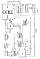
- Fig 1 is a section of a schematic representation of a facsimile apparatus, incorporating a digital reading device embodying the invention.
- Fig 2 is a plan of the apparatus along the line II-II of Fig 1;
- Fig 3 is a block diagram of the circuit for generating the signals of the reading device.
- a transparent support plate 10 for a document 11 (Fig 2) to be read is fixed and is covered with a hinged cover 12 (Fig 1), suitable for holding the document 11 against the plate 10.
- a keyboard 13 Adjacent to the cover 12 is placed a keyboard 13 for control of the digital reader.
- the lamps 14 are selected in such a way as to supply collectively a substantially constant distribution of spectral energy versus wavelength in the field of vision.
- two lamps of the company Toshiba have been selected, one lamp 14 being of blue colour and the other of white colour with cold light, designated EDCW by Toshiba.
- the carriage 16 carries a mirror 17 inclined at 45°, so as to reflect the image of the elementary line of the document in a plane parallel to the document itself, as indicated by the broken line in Fig 1.
- the reader comprises also a second carriage 18 carrying a pair of mirrors 19 and 21 inclined 45° in opposite directions, so as to reflect the optical beam 180° towards an objective 22. This focuses the beam on to a series of reading elements constituted by cells of a charge coupled device 23 (CCD).
- CCD charge coupled device
- the optical beam can be filtered by a colour filter selected from a number of filters carried by a disc 24.
- a colour filter selected from a number of filters carried by a disc 24.
- This can be rotated by a stepping electric motor 26 in order to select from one time to the next the required filter.
- the disc 24 comprises position without a filter for reading in black and white and three positions with red, green and blue filters for the reading of the respective colours.
- the cells of the CCD 23 are so spaced that each element can receive the light reflected by a small area of the document, called a pixel.
- the number of pixels per mm generally between 3 and 12, determines the horizontal resolution of the reading device.
- the number of lines per mm read on the document on the other hand determines the vertical resolution of the reader.
- the device may comprises a CCD 23 with 2048 cells, by means of which a 210 mm line is read with a resolution of 10 points/mm.
- the cells of the CCD 23 generate electrical signals corresponding to the intensity of light received, which after being serialized and then filtered and amplified by a circuit 27 (Fig 3) are sent to an analogue-digital converter 28 having for example a resolution of 6 bits, through which 64 levels of amplitude of reading signal can be identified.
- the converter 28 is of the fast type, known as a flash A/D converter.
- the digital signals can be coded, transmitted, stored and/or reproduced on paper.
- the ideal conditions for a correct reading would require a light source 14 (Fig 1) which is homogeneous along the line, an objective 22 devoid of losses at the edges, a constant reflectance of the mirrors 17, 19 and 21 and a perfect homogeneity of response of the different cells of the CCD 23.
- the reading device comprises a read/write memory (RAM) 31 (Fig 3), to store the signals obtained in a preliminary reading of the sample strip 29, and means for comparison comprising a programmable read only memory (EPROM) 32 to compare the reading signals of the individual elementary lines of the document 11 with the signals stored in the RAM 31. Therefore the RAM 31 has a capacity of at least 2X6K bits.
- the reading device comprises a central processing unit (CPU)33 with a microprocessor, which when it receives a command for reading the document 11, generated by the keyboard 13, executes a programme recorded in a read only memory (ROM) 34.
- the CPU 33 controls a circuit 36 for controlling the CCD 23, via a logic signal EXP corresponding to the duration of the enablement of the CCD for reading the document.
- the circuit 36 in response to the logic signal EXP, generates an analogue signal ⁇ X, which determines the duration of the enablement of the CCD 23, and a timing signal ⁇ T, which determines the serialisation of the signals generated by the CCD 23, to be sent to the circuit 27.
- the circuit 36 also generates a logic signal LN at every elementary line read and a logic signal CK at every pixel signal sent by the CCD 23 to the circuit 27. These two signals are sent to a counter 37, whose capacity is equal to the number of cells of the CCD 23 and hence to the number of pixels of an elementary line. The counter 37 thus indicates the position of the pixel whose signal is sent to the circuit 27. The output of the counter 37 addresses the successive locations of the RAM 31 in which the signals provided by the converter 28 are to be written or from which the signals stored there are to be read.
- the CPU 33 also generates, at the beginning of the reading routine given by the ROM 34, a signal C for a compensation command, which controls a circuit 38 for enablement of writing in the RAM 31.
- This circuit is further controlled by the signals LN and CK so as to emit the write-enable signal WR during the reading of the sample strip 29 (Fig 2).
- the signals of this reading, emitted by the converter 28 (Fig 3) are recorded in the RAM 31 at the addresses given by the counter 37.
- the signals emitted by the converter 28 are no longer stored by the RAM 31 and the counter 37 only addresses the cells of RAM 31 for reading from one line to the next.
- the CPU further provides two signals C1 and C2 indicative of the colour of the filter, according to the following table:
- the signals C1 and C2 control a circuit 39 for selection of the filter; this circuit controls the rotation of the stepping motor 26 (Fig 1) in a manner known per se.
- the EPROM 32 (Fig 3) is constituted by four modules associated with the four colours defined before.
- the four modules are addressed in parallel with 12 bits, six of which are supplied by the converter 28 in the direct reading of each pixel of the lines of the document 11, while the other six are supplied by the reading of the RAM 31 at the address given by the counter 37, whereby these represent the signals given by the converter 28 in the reading of the corresponding pixel of the sample line.
- each module of the EPROM 32 at each address there is recorded in advance a 4-bit value proprotional to the ratio between the direct reading signal of a pixel and that recorded in the RAM 31 in the preliminary reading of the corresponding pixel of the sample strip 29.
- the value recorded in the EPROM 32 is obtained by multiplying a number equal to the desired level number for the amplitude of the reading signal by the ratio between the value of the direct reading expressed by the six address bits supplied by the converter 28 and the value of the preliminary reading expressed by the six address bits supplied by the RAM 31.
- each module of the EPROM 32 there is constructed a true andd proper table of compensated values of reflectance compared with an address formed by six pre-stored bits in the RAM 31 and by six bits relating to the immediate reading of the pixels of the document.
- These values represent therefore the signals of the pixels compensated in amplitude for all the deteriorations of these occurring with time and with transverse location, through non-homogeneity of the lighting of the original, through dust deposition on the mirrors, through loss at the edges of the objective and through the non-homogeneity of the cells of the CCD.
- the four modules of the EPROM 32 permit the adoption of different compensations for the three primary colours and for black.
- the values thus address on the four modules of the EPROM 32 are sent to a multiplexer 41, which under the control of the two signals C1 and C2 sends to a circuit 42 for coding greys of half tones only those relating to the colour selected by these signals.
- the circuit 42 is also organised in four modules, one for each colour, selectable by the same signals C1 and C2. For each value given by the four bits of the multiplexer 41, the circuit 42 selects a corresponding sequence of bits indicative of the white and coloured points, to represent the corresponding value of the half tone, in a manner in itself known.
- the signals generated by the circuit 42 are then parallelised by a paralleliser 43 and are stored in a line buffer 44, under the control of an enablement signal DS emitted by the CPU 33 only when the scanning of the document 11 is effected. From the buffer 44 the stored signals are then taken for compression and subsequent storage in a mass or transmission memory to a distant station, or for controlling a device for reproduction of the image read.
- the EPROM 32 also supplies the four bits recorded at the address represented by two equal groups of six bits. Since, however, the CPU 33 does not emit the signal DS, these values are not stored in the buffer 44.
- the programme recorded in the ROM 34 comprises a routine for reading in black and white and a routine for reading in colour.
- the two routines are selected by means of the keyboard 13.
- the routine for reading in black and white makes the device execute a single reading cycle, in which the corresponding white position of the filter 24 is selected.
- the sample line 29 (Fig 2) is read, which is stored in the RAM 31 (Fig 3).
- the lines of the document 11 are read one after the other, whose values are compensated in amplitude by the B/W module in the EPROM 32.
- the routine for reading in colour makes the device execute three successive cycles of reading of the document 11, making the CPU 33 generate successively the values of the signals C1 and C2 which indicate red, green and blue.
- the device by means of the circuit 39, first selects the corresponding filter of the disc 24 (Fig 2). Then it reads with this filter the sample line 29, storing the signals in the RAM 31 (Fig 3). Finally it reads with the same filter the successive lines of the document 11 and, by means of the appropriate module of the EPROM 32, it suppleis the reading signals of the corresponding colour, compensated in amplitude.
- the device described can have various modifications and improvements made to it within the scope of the claims.
- the EPROM 32 can be replaced by a ROM or by any circuit suitable for supplying in output numerical or analogue values, as a function of the result of the comparison between the signals obtained in the reading of the sample line and those obtained in the direct reading of the lines of the document.
- the value recorded corresponding to each address of the compensation memory can be multiplied by a factor K which takes account of the particular use of the signal, for example for a video or for a print-out according to a specific technology. In that case, whenever the utilisation of the signals of the device is changed, it is necessary to replace the compensation memory.
- the device can be fitted with a number of compensation memories, automatically selectable as a function of the use of the signal chosen from time to time.
Landscapes
- Engineering & Computer Science (AREA)
- Multimedia (AREA)
- Signal Processing (AREA)
- Facsimile Scanning Arrangements (AREA)
- Facsimile Image Signal Circuits (AREA)
Claims (6)
- Farbbildlesevorrichtung mit Kompensation von Ungleichförmigkeit des Fotosensorsystems, aufweisend eine Lichtquelle (14) zum Beleuchten eines das zu lesende Bild tragenden Dokuments, einer Richtungseinrichtung (17, 19, 21, 22) zum Richten eines Streifens des so beleuchteten Bildes auf eine Serie von Leseelementen (23), um eine Folge von Antwortsignalen ansprechend auf eine Folge von Pixeln entlang des Streifens zu erzeugen, wobei die Richtungseinrichtung zumindest einen Spiegel (17, 19, 21) und ein Objektiv (22) umfaßt und die Serie von Leseelementen (23) eine Serie von Zellen eines Ladungsspeicherelements (CCD) umfaßt, einen A/D Wandler (28), der die Antwortsignale zur Lieferung entsprechender digitaler Signale bearbeitet, eine Speichereinrichtung (31) zum zeitweisen Speichern der digitalen Signale, die vom Wandler in einer vorab erfolgenden Lesung eines kalibrierten Hintergrund-Probestreifens (29) gewonnen werden, eine Nur-Lese-Speichereinrichtung (32), die sequentiell für jedes Bildpixel durch beide, die digitalen, vom Wandler beim Lesen eines Streifens des Dokumentenbildes gelieferten Signale und die entsprechenden in der Speichereinrichtung gespeicherten, digitalen Signale adressierbar ist, um Ausgangssignale zu liefern, die hinsichtlich Änderungen der Übertragungsfunktionen der Lichtquelle (14), des(r) Spiegel (17, 19, 21), des Objektivs (22) und des CCD's kompensierte Pixel darstellen, gekennzeichnet durch eine Anzahl Filter (24), die zur Einfügung zwischen dem Bild und dem CCD selektierbar sind, um das CCD dazu zu veranlassen, sequentiell eine Folge von einem jeden der Filter zugeordneten digitalen Signalen in der vorab erfolgenden Lesung zur Speicherung in der Speichereinrichtung zu erzeugen, und daß die Nur-Lese-Speichereinrichtung (32) eine dieser Anzahl von Filtern (24) entsprechende Anzahl von Abschnitten umfaßt, wobei jeder Abschnitt für jedes Bildpixel durch die digitalen Signale, die in einem Lesen eines Streifens dieses Bildes durch das zugeordnete Filter gewonnen wurden, und die entsprechenden digitalen Signale, die in der Speichereinrichtung (31) gespeichert sind, gemeinsam adressiert wird, wobei jeder Abschnitt der Nur-Lese-Speichereinrichtung (32) Ausgangssignale liefert, die entsprechend den zugeordneten Filtern unterschiedlich kompensierte Pixel repräsentieren.
- Vorrichtung nach Anspruch 1, gekennzeichnet durch eine Halbton-Codiereinrichtung (42), die eine Anzahl von den Abschnitten der Nur-Lese-Speichereinrichtung (32) zugeordneten Abschnitten aufweist, wobei jeder Abschnitt der Codiereinrichtung durch die von dem zugeordneten Abschnitt der Nur-Lese-Speichereinrichtung gelieferten Ausgangssignale gesteuert wird, um selbige entsprechend einem Muster von schwarzen und weißen Pixeln, das den entsprechenden, für die zugeordnete Farbe gewünschten Graupegel anzeigt, zu codieren.
- Vorrichtung nach Anspruch 2, gekennzeichnet durch eine manuelle Einrichtung (13), die betätigbar ist, um die sequentielle Selektion der Filter (24) und das wiederholte Lesen des Probestreifens (29) auszuschalten, wobei die Nur-Lese-Speichereinrichtung (32) einen zusätzlichen Abschnitt umfaßt, der zur Lieferung von hinsichtlich eines schwarzen und weißen Bildes kompensierten Ausgangssignalen adressierbar ist, und wobei die Codiereinrichtung (42) einen entsprechenden zusätzlichen Abschnitt zur Halbtoncodierung der von diesem zusätzlichen Abschnitt gelieferten Ausgangssignale umfaßt.
- Vorrichtung nach Anspruch 3, dadurch gekennzeichnet, daß der gespeicherte Wert proportional zum Verhältnis zwischen dem direkten Lesesignal eines Pixels und dem im vorab erfolgenden Lesen des entsprechenden Pixels vom Probestreifen (29) aufgezeichneten ist.
- Vorrichtung nach Anspruch 4, dadurch gekennzeichnet, daß der im Nur-Lese-Speicher (32) gespeicherte Wert durch Multiplizieren einer Zahl gleich der Zahl der gewünschten Graupegel mit dem Verhältnis zwischen dem Wert der direkten Lesung und dem Wert der vorab erfolgenden Lesung, ausgedrückt durch die jeweiligen Adressensignale, gewonnen wird.
- Vorrichtung nach Anspruch 5, in der die Grausignale von einer Vielfalt grafischer Apparate verwendet werden können, dadurch gekennzeichnet, daß mehrere Nur-Lese-Speicher (32) den verschiedenen Apparaten zugeordnet sind und für den Betrieb individuell selektierbar sind, wobei die in jedem Nur-Lese-Speicher gespeicherten Werte mit einem dem zugeordneten grafischen Apparat entsprechenden Faktor multipliziert werden.
Applications Claiming Priority (2)
| Application Number | Priority Date | Filing Date | Title |
|---|---|---|---|
| IT67407/85A IT1183816B (it) | 1985-05-03 | 1985-05-03 | Dispositivo di lettura digitale di documenti per apparecchiature di trasmissioni e o riproduzione di immagini con compensazione in ampiezza dei segnali di lettura |
| IT6740785 | 1985-05-03 |
Publications (3)
| Publication Number | Publication Date |
|---|---|
| EP0200438A2 EP0200438A2 (de) | 1986-11-05 |
| EP0200438A3 EP0200438A3 (en) | 1988-06-29 |
| EP0200438B1 true EP0200438B1 (de) | 1991-07-10 |
Family
ID=11302132
Family Applications (1)
| Application Number | Title | Priority Date | Filing Date |
|---|---|---|---|
| EP86302945A Expired EP0200438B1 (de) | 1985-05-03 | 1986-04-18 | Digitale Lesevorrichtung für Faksimilegeräte |
Country Status (5)
| Country | Link |
|---|---|
| US (1) | US4833533A (de) |
| EP (1) | EP0200438B1 (de) |
| JP (1) | JPS61263357A (de) |
| DE (1) | DE3680142D1 (de) |
| IT (1) | IT1183816B (de) |
Families Citing this family (27)
| Publication number | Priority date | Publication date | Assignee | Title |
|---|---|---|---|---|
| US5121230A (en) * | 1987-01-19 | 1992-06-09 | Canon Kabushiki Kaisha | Image reading apparatus having adjusting circuits for matching the level of and compensating for fluctuation among a plurality of sensing elements |
| US4945405A (en) * | 1987-05-21 | 1990-07-31 | Minolta Camera Kabushiki Kaisha | Color image read apparatus with shading and color balance correction |
| US5430559A (en) * | 1988-12-22 | 1995-07-04 | Minolta Camera Kabushiki Kaisha | Image reading apparatus with improved output correction of image signal |
| US4987485A (en) * | 1988-12-22 | 1991-01-22 | Minolta Camera Kabushiki Kaisha | Image reading apparatus with improved output correction of image signal |
| US5268752A (en) * | 1989-06-12 | 1993-12-07 | Semiconductor Energy Laboratory Co., Ltd. | Image sensing device utilizing synchronized LEDs and light sensors |
| GB2243515A (en) * | 1990-04-11 | 1991-10-30 | Rank Cintel Ltd | Digital video signal processing using lookup tables |
| US5109273A (en) * | 1990-05-11 | 1992-04-28 | Eastman Kodak Company | Signal processing circuit for performing a pipelined matrix multiplication upon signals from several linear sensors |
| US5047861A (en) * | 1990-07-31 | 1991-09-10 | Eastman Kodak Company | Method and apparatus for pixel non-uniformity correction |
| FR2670067A1 (fr) * | 1990-11-30 | 1992-06-05 | Scanera Sc | Dispositif de prise d'images d'une scene. |
| US5216525A (en) * | 1990-12-19 | 1993-06-01 | Ncr Corporation | Table top hardware for imaging documents |
| US5202767A (en) * | 1990-12-26 | 1993-04-13 | Pathology Imaging Corporation | Multimode computerized multicolor camera and method therefor |
| US5295003A (en) * | 1991-03-13 | 1994-03-15 | Lee Aldric K | Color conversion system for monochromatic optical scanner |
| US5149960B1 (en) * | 1991-07-03 | 1994-08-30 | Donnelly R R & Sons | Method of converting scanner signals into colorimetric signals |
| US5495429A (en) * | 1993-02-12 | 1996-02-27 | West Virginia University | Method and apparatus for measuring the color of three dimensional objects |
| US5729361A (en) * | 1995-06-30 | 1998-03-17 | Logitech, Inc. | Color scanner using both variable led exposure time and photo detector output compensation |
| JPH09181903A (ja) * | 1995-12-22 | 1997-07-11 | Fuji Photo Film Co Ltd | 画像再生方法および装置 |
| KR0181157B1 (ko) * | 1996-04-10 | 1999-05-01 | 김광호 | 중간조처리 및 쉐이딩 보정을 위한 화상 처리장치 및 그 방법 |
| GB2316259B (en) * | 1996-08-12 | 2000-09-06 | Alps Electric Co Ltd | Image sensing apparatus and shading correction method |
| US6167469A (en) | 1998-05-18 | 2000-12-26 | Agilent Technologies, Inc. | Digital camera having display device for displaying graphical representation of user input and method for transporting the selected digital images thereof |
| US6577336B2 (en) | 1998-05-29 | 2003-06-10 | Agilent Technologies, Inc. | Authentication stamping in a digital camera |
| US6593963B1 (en) | 1998-05-29 | 2003-07-15 | Agilent Technologies, Inc. | Programmable control of operational signals in a digital camera |
| US6642956B1 (en) * | 1998-05-29 | 2003-11-04 | Agilent Technologies, Inc. | Digital image processor for a digital camera |
| GB2372392A (en) * | 2001-02-16 | 2002-08-21 | Hewlett Packard Co | Improvements to image capture |
| US7012633B2 (en) * | 2002-03-06 | 2006-03-14 | Radiant Imaging, Inv. | Color calibration method for imaging color measurement device |
| US7199843B2 (en) * | 2002-09-30 | 2007-04-03 | Lsi Logic Corporation | Spectral translation for VSB compensation |
| US7545543B2 (en) * | 2004-12-09 | 2009-06-09 | Xerox Corporation | Scanner illuminator systems and methods |
| US8555065B2 (en) * | 2011-08-24 | 2013-10-08 | Jeffrey Thomas CESNIK | Method and apparatus for transmitting, receiving and decoding data using encoded patterns of changing colors |
Family Cites Families (14)
| Publication number | Priority date | Publication date | Assignee | Title |
|---|---|---|---|---|
| US3800078A (en) * | 1972-12-18 | 1974-03-26 | Ibm | Digitally compensated scanning system |
| JPS5579567A (en) * | 1978-12-12 | 1980-06-16 | Ricoh Co Ltd | Shading correction system |
| JPS55112685A (en) * | 1979-02-22 | 1980-08-30 | Nec Corp | Picture input unit |
| JPS5658370A (en) * | 1979-10-18 | 1981-05-21 | Ricoh Co Ltd | Read-in method for color picture |
| JPS58177071A (ja) * | 1982-04-09 | 1983-10-17 | Fuji Xerox Co Ltd | シエ−デイング補正装置 |
| JPS5927675A (ja) * | 1982-08-04 | 1984-02-14 | Toshiba Corp | シエ−デイング補正方式 |
| JPH0683371B2 (ja) * | 1982-10-20 | 1994-10-19 | キヤノン株式会社 | 情報読取り装置 |
| JPS5979676A (ja) * | 1982-10-27 | 1984-05-08 | Canon Inc | 多色画像情報読み取り装置 |
| JPS59161978A (ja) * | 1983-03-06 | 1984-09-12 | Canon Inc | 画像処理装置 |
| US4727434A (en) * | 1984-03-14 | 1988-02-23 | Canon Kabushiki Kaisha | Image processing apparatus for rapid production of a hard copy of a video image in which input image signal processing parameters are set while a record medium is being positioned at a recording position |
| US4647961A (en) * | 1984-07-23 | 1987-03-03 | Ricoh Company Ltd. | Apparatus for reading the image information of a colored original |
| US4731661A (en) * | 1984-11-16 | 1988-03-15 | Sharp Kabushiki Kaisha | Color document reader with white balance adjuster for determining light emission periods for a plurality of different-colored light sources and corresponding integration times for a light sensor by reading a white reference area |
| JPH05252523A (ja) * | 1992-03-03 | 1993-09-28 | Miyota Kk | 小型カラービューファインダ |
| JPH0696955A (ja) * | 1992-03-31 | 1994-04-08 | Matsushita Electric Ind Co Ltd | コイルおよびその製造方法 |
-
1985
- 1985-05-03 IT IT67407/85A patent/IT1183816B/it active
-
1986
- 1986-04-18 DE DE8686302945T patent/DE3680142D1/de not_active Expired - Lifetime
- 1986-04-18 EP EP86302945A patent/EP0200438B1/de not_active Expired
- 1986-05-02 US US06/858,929 patent/US4833533A/en not_active Expired - Fee Related
- 1986-05-02 JP JP61102919A patent/JPS61263357A/ja active Pending
Also Published As
| Publication number | Publication date |
|---|---|
| IT8567407A0 (it) | 1985-05-03 |
| US4833533A (en) | 1989-05-23 |
| IT1183816B (it) | 1987-10-22 |
| EP0200438A3 (en) | 1988-06-29 |
| JPS61263357A (ja) | 1986-11-21 |
| DE3680142D1 (de) | 1991-08-14 |
| EP0200438A2 (de) | 1986-11-05 |
Similar Documents
| Publication | Publication Date | Title |
|---|---|---|
| EP0200438B1 (de) | Digitale Lesevorrichtung für Faksimilegeräte | |
| US4583186A (en) | Computerized video imaging system | |
| US4424589A (en) | Flat bed scanner system and method | |
| JP2817932B2 (ja) | 画像読取装置 | |
| US4415925A (en) | Color original readout apparatus | |
| US4814877A (en) | Image reading apparatus provided with correction for shadings in image data | |
| JP3175190B2 (ja) | 画像読取装置及びカラーバランス設定装置 | |
| US6078684A (en) | Color image scanning device | |
| USRE33244E (en) | Computerized video imaging system | |
| JP2973596B2 (ja) | 画像読取装置 | |
| JPS59223060A (ja) | 原稿読取装置 | |
| JP3168020B2 (ja) | 画像読取装置および方法 | |
| JPH01108860A (ja) | 画像読取装置 | |
| JPH01147963A (ja) | 画像読取り装置 | |
| JPH05219369A (ja) | 画像読み取り装置 | |
| JPH04320159A (ja) | 画像読取装置 | |
| JPH0197053A (ja) | 多色画像処理装置 | |
| JPH0197050A (ja) | 多色画像処理装置 | |
| JPS62202673A (ja) | 画像情報読取り装置 | |
| JPH07131645A (ja) | 画像読み取り装置 | |
| JPH08235055A (ja) | メモリ制御装置 | |
| JPH1023283A (ja) | 画像読み取り装置 | |
| JPS62202653A (ja) | シエ−デイング補正方法 | |
| JPH04318757A (ja) | 画像読取装置 | |
| JPH03259664A (ja) | 原稿入力装置 |
Legal Events
| Date | Code | Title | Description |
|---|---|---|---|
| PUAI | Public reference made under article 153(3) epc to a published international application that has entered the european phase |
Free format text: ORIGINAL CODE: 0009012 |
|
| AK | Designated contracting states |
Kind code of ref document: A2 Designated state(s): DE FR GB |
|
| PUAL | Search report despatched |
Free format text: ORIGINAL CODE: 0009013 |
|
| AK | Designated contracting states |
Kind code of ref document: A3 Designated state(s): DE FR GB |
|
| 17P | Request for examination filed |
Effective date: 19881121 |
|
| 17Q | First examination report despatched |
Effective date: 19900927 |
|
| GRAA | (expected) grant |
Free format text: ORIGINAL CODE: 0009210 |
|
| AK | Designated contracting states |
Kind code of ref document: B1 Designated state(s): DE FR GB |
|
| REF | Corresponds to: |
Ref document number: 3680142 Country of ref document: DE Date of ref document: 19910814 |
|
| ET | Fr: translation filed | ||
| PLBE | No opposition filed within time limit |
Free format text: ORIGINAL CODE: 0009261 |
|
| STAA | Information on the status of an ep patent application or granted ep patent |
Free format text: STATUS: NO OPPOSITION FILED WITHIN TIME LIMIT |
|
| 26N | No opposition filed | ||
| PGFP | Annual fee paid to national office [announced via postgrant information from national office to epo] |
Ref country code: GB Payment date: 19930407 Year of fee payment: 8 |
|
| PGFP | Annual fee paid to national office [announced via postgrant information from national office to epo] |
Ref country code: FR Payment date: 19930408 Year of fee payment: 8 |
|
| PGFP | Annual fee paid to national office [announced via postgrant information from national office to epo] |
Ref country code: DE Payment date: 19930506 Year of fee payment: 8 |
|
| PG25 | Lapsed in a contracting state [announced via postgrant information from national office to epo] |
Ref country code: GB Effective date: 19940418 |
|
| GBPC | Gb: european patent ceased through non-payment of renewal fee |
Effective date: 19940418 |
|
| PG25 | Lapsed in a contracting state [announced via postgrant information from national office to epo] |
Ref country code: FR Effective date: 19941229 |
|
| PG25 | Lapsed in a contracting state [announced via postgrant information from national office to epo] |
Ref country code: DE Effective date: 19950103 |
|
| REG | Reference to a national code |
Ref country code: FR Ref legal event code: ST |