EP0199303A2 - Procédé pour obtenir des structures formant un agent de photoréserve - Google Patents
Procédé pour obtenir des structures formant un agent de photoréserve Download PDFInfo
- Publication number
- EP0199303A2 EP0199303A2 EP19860105373 EP86105373A EP0199303A2 EP 0199303 A2 EP0199303 A2 EP 0199303A2 EP 19860105373 EP19860105373 EP 19860105373 EP 86105373 A EP86105373 A EP 86105373A EP 0199303 A2 EP0199303 A2 EP 0199303A2
- Authority
- EP
- European Patent Office
- Prior art keywords
- coating film
- photoresist
- photoresist pattern
- forming
- exposed
- Prior art date
- Legal status (The legal status is an assumption and is not a legal conclusion. Google has not performed a legal analysis and makes no representation as to the accuracy of the status listed.)
- Granted
Links
Images
Classifications
-
- G—PHYSICS
- G03—PHOTOGRAPHY; CINEMATOGRAPHY; ANALOGOUS TECHNIQUES USING WAVES OTHER THAN OPTICAL WAVES; ELECTROGRAPHY; HOLOGRAPHY
- G03F—PHOTOMECHANICAL PRODUCTION OF TEXTURED OR PATTERNED SURFACES, e.g. FOR PRINTING, FOR PROCESSING OF SEMICONDUCTOR DEVICES; MATERIALS THEREFOR; ORIGINALS THEREFOR; APPARATUS SPECIALLY ADAPTED THEREFOR
- G03F7/00—Photomechanical, e.g. photolithographic, production of textured or patterned surfaces, e.g. printing surfaces; Materials therefor, e.g. comprising photoresists; Apparatus specially adapted therefor
- G03F7/004—Photosensitive materials
- G03F7/022—Quinonediazides
-
- G—PHYSICS
- G03—PHOTOGRAPHY; CINEMATOGRAPHY; ANALOGOUS TECHNIQUES USING WAVES OTHER THAN OPTICAL WAVES; ELECTROGRAPHY; HOLOGRAPHY
- G03F—PHOTOMECHANICAL PRODUCTION OF TEXTURED OR PATTERNED SURFACES, e.g. FOR PRINTING, FOR PROCESSING OF SEMICONDUCTOR DEVICES; MATERIALS THEREFOR; ORIGINALS THEREFOR; APPARATUS SPECIALLY ADAPTED THEREFOR
- G03F7/00—Photomechanical, e.g. photolithographic, production of textured or patterned surfaces, e.g. printing surfaces; Materials therefor, e.g. comprising photoresists; Apparatus specially adapted therefor
- G03F7/20—Exposure; Apparatus therefor
- G03F7/2002—Exposure; Apparatus therefor with visible light or UV light, through an original having an opaque pattern on a transparent support, e.g. film printing, projection printing; by reflection of visible or UV light from an original such as a printed image
- G03F7/2004—Exposure; Apparatus therefor with visible light or UV light, through an original having an opaque pattern on a transparent support, e.g. film printing, projection printing; by reflection of visible or UV light from an original such as a printed image characterised by the use of a particular light source, e.g. fluorescent lamps or deep UV light
-
- G—PHYSICS
- G03—PHOTOGRAPHY; CINEMATOGRAPHY; ANALOGOUS TECHNIQUES USING WAVES OTHER THAN OPTICAL WAVES; ELECTROGRAPHY; HOLOGRAPHY
- G03F—PHOTOMECHANICAL PRODUCTION OF TEXTURED OR PATTERNED SURFACES, e.g. FOR PRINTING, FOR PROCESSING OF SEMICONDUCTOR DEVICES; MATERIALS THEREFOR; ORIGINALS THEREFOR; APPARATUS SPECIALLY ADAPTED THEREFOR
- G03F7/00—Photomechanical, e.g. photolithographic, production of textured or patterned surfaces, e.g. printing surfaces; Materials therefor, e.g. comprising photoresists; Apparatus specially adapted therefor
- G03F7/26—Processing photosensitive materials; Apparatus therefor
- G03F7/30—Imagewise removal using liquid means
- G03F7/32—Liquid compositions therefor, e.g. developers
- G03F7/325—Non-aqueous compositions
Definitions
- the present invention relates to a method of forming a photoresist pattern.
- the photoresist pattern is specifically used for manufacturing semiconductor devices with the submicrometer resolution.
- One of the fine processing methods employs ionization radiation such as electron beams, X-rays, shortwavelength ultraviolet radiation and the like so as to form the photoresist pattern, and thereafter precisely transfer the photoresist pattern onto underlying layers, e.g., substrates by dry-etching treatment in which ion or plasma has been filled.
- ionization radiation such as electron beams, X-rays, shortwavelength ultraviolet radiation and the like
- a transfer apparatus for forming a photoresist pattern for a fine process As a transfer apparatus for forming a photoresist pattern for a fine process, as an optical reduction type transfer apparatus (aligner) has been mainly used because the equipment of its properties of high resolution and high accuracy for alignment.
- As a light source of this type of transfer apparatus g-line emitted from the mercury vaper lamp and being in a region of near ultraviolet region is most expected in view of lower absorption in the optical system and higher light outputs.
- a photoresist for photolithography using the near ultraviolet radiation, due to high resolution and dry etching resistance, a photoresist is used which is obtained by mixing novolak resin and naphthoquinone diazide of a photosensitive material. Further, as- a negative type photoresist, a photoresist obtained by mixing polyvinyl phenol and bisazide is used. This resist has high sensitivity at i-line (365 nm).
- the sensitivity of the above negative type photoresist is low.
- the positive type photoresists have difficulty in maintaining good line width control over the topography because of the reflective notching caused by reflected light from the substrate.
- the negative and positive type photoresist patterns are able to be formed only by selecting developing solutions, it is possible to select a method by which the negative or positive type photoresist pattern can be easily obtained in accordance with the photoresist pattern. As a result, various merits are achieved in the manufacturing of semiconductor devices.
- the object of the invention may be accomplished by providing a method of forming a photoresist pattern according to the following steps.
- a coating film of naphthoquinone diazide sulfonate of novolak as a photoresist coating film is firstly formed on a substrate or other underlying layer.
- this coating film is exposed by irradiating with near ultraviolet radiation of from 300 to 450 nm through a photomask of a desirable pattern which is to be copied to the coating film.
- the light wavelength is below 300 nm, a negative pattern can be formed, but a positive pattern can not be formed. If the light wavelength is above 450 nm, the resist is not sensitized. Accordingly, the light source having the above wavelength region is used.
- the irradiated coating film is developed with a negative type developing solution.
- the positive pattern is formed, the irradiated coating film is developed with positive type developing solution.
- the negative type developing solution is preferably a solution which is made by mixing the nonpolar solvent with one or more solutions selected from the group consisting of cyclohexane, n-hexane and petroleum ether.
- the halogen-containing solvent is also able to consist of one or more solvents selected from the group consisting of monochlorobenzene, trichloroethylene, chloroform, dichloromethane and dichloroethane..
- the alkyl benzene solvent is also able to consist of one or more solvents selected from the group consisting of xylene, toluene and benzene.
- the positive type developing solution preferably contains one or more solvents selected from the group consisting of alcohol solvents, mixed solvents of acetate and alcohol, and mixed solvents of alkyl ketones and alcohol.
- the alcohol sptvent is able to consist of one or more solvents selected from the group consisting of isopropyl alcohol, n-butyl alcohol and methanol.
- isoamyl acetate from the group of the acetates and also to select methylisobutyl ketone from the group of the alkyl ketones.
- the present invention is able to form the photoresist coating film of naphthoquinone diazide sulfonate of novolak, expose the photoresist coating film by irradiating with near ultraviolet radiation, and selectively use negative or positive type developing solution for the exposed photoresist coating film in accordance with a desirable pattern to be formed.
- NQN naphthoquinone diazide sulfonate of novolak
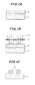
- this silicon wafer 1 having a photoresist coating film 2 of NQN was prebaked at a temperature of 70°C for about 30 minutes. Thereafter, the resist coating film 2 of NQN was treated by exposing with the g-line of a 250 W mercury lamp of the 1/5 optical reduction type aligner (not shown in detail). The exposure dose was 50 mJ/cm 2 . Accordingly, a photomask pattern 3 was transferred onto the NQN coating film 2. Thereafter, the wafer 1 having the exposed NQN coating film 2 was interbaked at a temperature range of 60 to 130°C, preferably 100°C for approximately 30 minutes.
- Such an interbaking treatment to the exposed NQN coating film 2 increases its sensitivity without lowering its resolution.
- this NQN coating film 2 was developed for 35 seconds by employing a mixutre type developing solution containing a volume rate of 10 : 1 of monochloro benzene and cyclohexane. The temperature of this developing solution was 23°C. Subsequently, the coating film 2 was rinsed in cyclohexane for 10 seconds, so that concaves (not shown) were formed in unexposed surface portions of the substrate or wafer 1, to which no ultraviolet radiation 10 had been projected because these portions were located under the photomask 3. Thus, a negative type photoresist pattern 5 was fabricated.
- Such a negative type photoresist pattern 5 could have clean, sharp and rectangular sectional plane and also resolved to a 0.6 ⁇ m line and space pattern by observing with a scanning electron microscope.
- a substrate consisting of a silicon water and an alminum layer formed thereon instead of the silicon wafer 1 as described in Fig. 1 was employed and the same film forming process as in the Example I was conducted.
- the recognition could be made in that the resultant photoresist pattern was resolved to a 0.7 nm line and space pattern by observing with the scanning electron microscope.
- the photoresist pattern fabricated according to the example I was baked at a temperature of 150°C for 30 minutes. The edge portion of the baked photoresist pattern was not deformed when observed by the scanning electron microscope.
- Az-1350J i.e., the photoresist commercially available from Shipley corporation
- the conventional photoresist pattern was baked at a temperature of 150°C, the edge portion thereof was deformed so that the sectional plane of the photoresist pattern was rounded.
- the photoresist film was formed according to the same method as in the Example I, and then exposed at the exposure dose of 100 mJ/cm 2 .
- the exposed film was developed by using a developing solution consisting of a 10 : 1 volume ratio of xylene to cyclohexane at a temperature of 23°C for 60 seconds. After the developed film was rinsed in cyclohexane, a negative type photoresist pattern could be obtained having the resolution of a 0.7 nm line and space.
- Naphthoquinone diazide sulfonate of novolak - (NQN) was dissolved into methyl cellosolve acetate at the rate of 25 weight %, this solution was then filtered through a filter having a throughhole diameter of 0.2 nm and applied onto the silicon wafer in a coating thickness of 0.8 ⁇ m by using a spin coating method.
- this silicon wafer having a photoresist coating of NQN was prebaked at a temperature of 60°C for about 30 minutes.
- the resist coating of NQN was treated by contact- exposing with a 250 W mercury lamp. The dose amount was 100 mJ/cm 2.
- the exposed film was developed by ussing trichloroethylene at a temperature of 23 ° C for 30 seconds and rinsed with cyclohexane at a temperature of 23°C for 15 seconds. Then a negative type photoresist pattern was obtained. It could be recognized that the negative type photoresist pattern was resolved to a 1.0 ⁇ m line and space pattern, and the thickness of the remaining coating film after development was 0.8 u.m.
- a coating of naphthoquinone diazide sulfonate of novolak (NQN) was formed and exposed as described in Example V.
- the coating was developed by using a solution containing 3 parts by weight of chloroform and 1 part by weight of cyclohexane at a temperature of 23 °C for 15 seconds, and rinsed with cyclohexane for 15 seconds.
- a negative type photoresist pattern was obtained. It could be recognized that the negative type photoresist pattern was resolved to a 1.0 ⁇ m line and space pattern. The thickness of the remaining coating film after the development was 0.78 n.m.
- a silicon - (Si) wafer 1 was prepared as a substrate. Naphthoquinone diazide sulfonate of novolak - (abbreviated as "NQN") as a photoresist material was used. This NQN was dissolved into methyl cellosolve acetate at a rate of 10 to 40 weight %. This solution was then filtered through a filter having a throughhole diameter of 0.2 ⁇ m and applied onto the silicon wafer 1, whereby the wafer 1 is coated by a film having a thickness of approximately 1 ⁇ m.
- NQN novolak -
- this silicon wafer 1 having a photo resist coating film 2 of NQN was prebaked at a temperature of 70°C for about 30 minutes. After this baking, the resist film 2 of NQN was exposed through a photoresist mask 3 having a desired mask pattern by a 1/5 optical reduction type transfer apparatus (NA : 0.35) equipped with g-line of 350 W mercury lamp as a light source. The dose time within one exposure process was determined as 450 msec.
- the resist film 2 formed on the substrate 1 was interbaked at a temperature on the order of 100°C for approximately 30 minutes, and then developed.
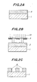
- FIG. 2A to 2C a description will be made of a second development with the same photoresist coating film 2 as in Figs. 1A to 1C.
- a mixed solution of a 1 : 1 volume ratio of isoamilacetic acid and isopropyl alcohol was used as a second developing solution.
- the coating film 2 was developed with this second solution at a temperature of 23 °C for 30 seconds.
- a positive type photoresist pattern 6 was formed. It could be recognized that the positive type pattern 6 was resolved to a 0.7 nm line and space pattern by similarly observing with the scanning electron microscope.
- the identical photoresist material can be employed to form either one of the negative and positive photoresist patterns by merely choosing sorts of the developing solutions.
- the resultant photoresist coating film as described in Example VII was contact- exposed with a mercury (Hg) lamp of 250 W.
- the exposure time was selected to be 10 seconds.
- the photoresist was developed at a temperature of 23 °C for 50 seconds using the mixed developing solution containing 1 : 0.15 volume ratio of monochlorobenzene and isopropyl alcohol, thereby a negative type photoresist pattern being obtained. It could be recognized that the negative type photoresist pattern was resolved to a 0.5 u.m line and space pattern by observing with the scanning electron microscope.
- the exposed photoresist coating film was developed at a temperature of 23 °C for 30 seconds by using the mixed developing solution containing a 1 : 1 volume ratio of isoamyl acetate and isopropyl alcohol. As a result, a positive type pattern photoresist was obtained. This positive type photoresist could be resolved to a 0.5 ⁇ m line and space.
- Another advantage is that, in case of froming the photoresist patterns on the reflective and/or steped surface of the underlying layer, the mask patterns are precisely transferred onto the photoresist coating film, thereby forming the correct, clean and sharp photoresist patterns, since the light absorption coefficient of the NQN film to the exposure radiation of the wavelength range of 300 to 450 nm is large and therefore the sensitivity of the NQN film is high and then the patterning precision is not influenced by the light reflected from the surface of the underlying layer.
- a further advantage is that the edge portions of the photoresist patterns are not deformed when baked at a temperature of the order of 200 °C since the NQN film has better heat resistance at a temperature of the order of 200 °C.
- a still further advantage is that the underlying layer having formed thereon the photoresist patterns can be subjected to the plasma etching treatment, since the NQN material has excellent resistance to the dryetching.
- the conventional photoresist of AZ-1305J - (commercially available from Shipley corporation) was coated over a silicon wafer with a coating thickness of 1.0 nm so as to form a photoresist film. Subsequently, the photoresist film was prebaked at a temperature of 80 °C for 20 minutes, and thereafter exposed under the exposure dose of 80 mJ/cm 2 by the same reduction type projection apparatus as in the Example I. When the exposed film was developed for 60 seconds by use of monochloro-benzene at a temperature of 23 °C as a developing solution, both the exposed portion and unexposed portion of the resist film were not dissolved, so that no photoresist pattern could be formed.
- a photoresist coating film of AZ-1350J was formed on an aluminum substrate under the same conditions as in the comparison example I, and then exposed.
- the exposed photoresist film was developed with an alkaline developing solution, the photoresist pattern having a linewidth more than or equal to 1 nm could be fabricated, but the pattern having a linewidth less than 1 u.m, i.e., submicrometer could not be formed.
- AZ-1350J photoresist commercially available from Shipley corporation
- AZ-1350J photoresist commercially available from Shipley corporation
- the exposed resist was developed by using a solution containing the AZ developing solution diluted with water at a ratio of 1 : 1 at a temperature of 23 °C for 20 seconds.
- a positive type photoresist pattern was obtained. Observing this resist pattern, it could be recognized that a 1.0 ⁇ m line and space pattern was obtained.
- Quinon diazide group of NQN is decomposed by the near ultraviolet radiation, and converted into carboxylic acid. Then, polarity appears in the exposed region of NQN. The polar region is not dissolved in monochloro benzene which is a nonpolar solvent. As a result, the negative type photoresist pattern is formed by the insoluble polar region.
- the only exposed and larger polar region of NQN is dissolved in the polar solvent, and the positive type photoresist pattern is formed by an insoluble region of NQN.
- the dissolution of the exposed portion of the photoresist coating film was done relatively faster than that of the unexposed portions thereof.
- the photoresist coating film represents the positive type property.
- a thickness of the remaining film was thinner than 0.1 ⁇ m.
- the unexposed portion of the photoresist coating film was not completely dissolved, whereas a thickness of the exposed portion thereof was approximately 0.1 u,m.
- the developing solutions used in the first to fourth development examples represent the positive type property. However, no photoresist pattern could be formed.
- the developing solutions there are preferable solutions except the above-described kinds of solutions.
- the positive type developing solutions polar solvents such as methanol, isopropyl alcohol and/or the other alcohols, isoamyl acetate and/or the other acetates, methylbutyl ketone and/or the other alkyl ketones, or the other desired developing solutions may be used.
- These developing solutions may be used by mixing one or more solvents selected from the group consisting of these alcohols, acetates and alkyl ketones.
- nonpolar solvents such as monochloro benzene , xylene, toluene, benzene, dichloro benzene, trichloro benzene, trichloro ethylene or the other preferable nonpolar solvents may be used.
- Mixed solutions of one or more nonpolar solvents selected from the above-mentioned group and one or more solvents selected from the group consisting of cyclohexane, n-hexane, petroleum ether and the other desired solvents may be used as the developing solutions.
- the coating film need not be directly coated on the substrate, but on other underlying layer.
- either positive type or negative type photoresist pattern can be formed by selecting only the developing solution because the naphthoquinone diazide sulfonate of novolak is used, and exposed to near ultraviolet radiation in the wavelength range of 300 to 450 nm.
- the photoresist pattern of the present invention is preferably used for manufacturing highly integrated circuit such as LSI which needs the fine processing, e.g., submicrometer processing.
Applications Claiming Priority (4)
| Application Number | Priority Date | Filing Date | Title |
|---|---|---|---|
| JP83070/85 | 1985-04-18 | ||
| JP60083070A JPS61241745A (ja) | 1985-04-18 | 1985-04-18 | ネガ型フオトレジスト組成物及びレジストパタ−ン形成方法 |
| JP169510/85 | 1985-07-31 | ||
| JP60169510A JPS6230322A (ja) | 1985-07-31 | 1985-07-31 | フオトレジストパタ−ンの形成方法 |
Publications (3)
| Publication Number | Publication Date |
|---|---|
| EP0199303A2 true EP0199303A2 (fr) | 1986-10-29 |
| EP0199303A3 EP0199303A3 (en) | 1987-12-23 |
| EP0199303B1 EP0199303B1 (fr) | 1992-06-24 |
Family
ID=26424141
Family Applications (1)
| Application Number | Title | Priority Date | Filing Date |
|---|---|---|---|
| EP86105373A Expired - Lifetime EP0199303B1 (fr) | 1985-04-18 | 1986-04-18 | Procédé pour obtenir des structures formant un agent de photoréserve |
Country Status (3)
| Country | Link |
|---|---|
| US (1) | US4801518A (fr) |
| EP (1) | EP0199303B1 (fr) |
| DE (1) | DE3685766T2 (fr) |
Families Citing this family (7)
| Publication number | Priority date | Publication date | Assignee | Title |
|---|---|---|---|---|
| US5024922A (en) * | 1988-11-07 | 1991-06-18 | Moss Mary G | Positive working polyamic acid/imide and diazoquinone photoresist with high temperature pre-bake |
| JPH08152716A (ja) * | 1994-11-28 | 1996-06-11 | Mitsubishi Electric Corp | ネガ型レジスト及びレジストパターンの形成方法 |
| JP4673513B2 (ja) * | 2001-08-01 | 2011-04-20 | 株式会社半導体エネルギー研究所 | 半導体装置の作製方法 |
| US7879696B2 (en) * | 2003-07-08 | 2011-02-01 | Kovio, Inc. | Compositions and methods for forming a semiconducting and/or silicon-containing film, and structures formed therefrom |
| KR101137845B1 (ko) * | 2005-06-24 | 2012-04-20 | 엘지디스플레이 주식회사 | 소프트 몰드의 제조방법 |
| WO2011139073A2 (fr) * | 2010-05-04 | 2011-11-10 | 주식회사 엘지화학 | Composition de résine photosensible négative et procédé destiné à un dispositif de formation de motifs |
| JP5618625B2 (ja) | 2010-05-25 | 2014-11-05 | 富士フイルム株式会社 | パターン形成方法及び感活性光線性又は感放射線性樹脂組成物 |
Citations (8)
| Publication number | Priority date | Publication date | Assignee | Title |
|---|---|---|---|---|
| US2697039A (en) * | 1953-10-26 | 1954-12-14 | Eastman Kodak Co | Preparation of lithographic printing plates |
| US2929708A (en) * | 1954-10-26 | 1960-03-22 | Gen Aniline & Film Corp | Phosphor screens for color television and method of preparing the same while using diazotype materials |
| GB844039A (en) * | 1959-02-20 | 1960-08-10 | Kalle & Co Ag | Improvements in or relating to photo-mechanical reproduction |
| US3046114A (en) * | 1955-03-01 | 1962-07-24 | Azoplate Corp | Diazo compounds and printing plates manufactured therefrom |
| US3635709A (en) * | 1966-12-15 | 1972-01-18 | Polychrome Corp | Light-sensitive lithographic plate |
| DE2504130A1 (de) * | 1974-01-31 | 1975-08-07 | Fuji Photo Film Co Ltd | Verfahren zum entwickeln einer lichtempfindlichen flachdruckplatte |
| US4212935A (en) * | 1978-02-24 | 1980-07-15 | International Business Machines Corporation | Method of modifying the development profile of photoresists |
| EP0110214A1 (fr) * | 1982-11-12 | 1984-06-13 | Fuji Photo Film Co., Ltd. | Composition photosensible |
Family Cites Families (8)
| Publication number | Priority date | Publication date | Assignee | Title |
|---|---|---|---|---|
| BE506677A (fr) * | 1950-10-31 | |||
| GB1136544A (en) * | 1966-02-28 | 1968-12-11 | Agfa Gevaert Nv | Photochemical cross-linking of polymers |
| US3644118A (en) * | 1970-08-31 | 1972-02-22 | Ibm | Polydiacrylyl photosensitive compositions |
| US4196003A (en) * | 1974-02-01 | 1980-04-01 | Fuji Photo Film Co., Ltd. | Light-sensitive o-quinone diazide copying composition |
| NL8100259A (nl) * | 1980-01-21 | 1981-08-17 | Wellcome Found | Combinaties van ketonen met heterocyclische verbindingen, famaceutische preparaten welke deze bevatten, werkwijze om dergelijke preparaten te bereiden en toepassing daarvan in de geneeskunde. |
| US4491628A (en) * | 1982-08-23 | 1985-01-01 | International Business Machines Corporation | Positive- and negative-working resist compositions with acid generating photoinitiator and polymer with acid labile groups pendant from polymer backbone |
| US4600684A (en) * | 1983-02-10 | 1986-07-15 | Oki Electric Industry Co., Ltd. | Process for forming a negative resist using high energy beam |
| US4609615A (en) * | 1983-03-31 | 1986-09-02 | Oki Electric Industry Co., Ltd. | Process for forming pattern with negative resist using quinone diazide compound |
-
1986
- 1986-04-18 EP EP86105373A patent/EP0199303B1/fr not_active Expired - Lifetime
- 1986-04-18 DE DE8686105373T patent/DE3685766T2/de not_active Expired - Fee Related
-
1987
- 1987-12-03 US US07/129,936 patent/US4801518A/en not_active Expired - Lifetime
Patent Citations (8)
| Publication number | Priority date | Publication date | Assignee | Title |
|---|---|---|---|---|
| US2697039A (en) * | 1953-10-26 | 1954-12-14 | Eastman Kodak Co | Preparation of lithographic printing plates |
| US2929708A (en) * | 1954-10-26 | 1960-03-22 | Gen Aniline & Film Corp | Phosphor screens for color television and method of preparing the same while using diazotype materials |
| US3046114A (en) * | 1955-03-01 | 1962-07-24 | Azoplate Corp | Diazo compounds and printing plates manufactured therefrom |
| GB844039A (en) * | 1959-02-20 | 1960-08-10 | Kalle & Co Ag | Improvements in or relating to photo-mechanical reproduction |
| US3635709A (en) * | 1966-12-15 | 1972-01-18 | Polychrome Corp | Light-sensitive lithographic plate |
| DE2504130A1 (de) * | 1974-01-31 | 1975-08-07 | Fuji Photo Film Co Ltd | Verfahren zum entwickeln einer lichtempfindlichen flachdruckplatte |
| US4212935A (en) * | 1978-02-24 | 1980-07-15 | International Business Machines Corporation | Method of modifying the development profile of photoresists |
| EP0110214A1 (fr) * | 1982-11-12 | 1984-06-13 | Fuji Photo Film Co., Ltd. | Composition photosensible |
Non-Patent Citations (5)
| Title |
|---|
| D.J. ELLIOTT: "Integrated Circuit Fabrication Technology", 1982, pages 165-207, Mc-Graw-Hill, New York, US; * |
| IBM TECHNICAL DISCLOSURE BULLETIN, vol. 14, no. 12, May 1972, page 3717, New York, US; M.W. MACINTYRE et al.: "Organic developer for positive photoresists" * |
| IBM TECHNICAL DISCLOSURE BULLETIN, vol. 16, no. 2, July 1973, page 426, New York, US; J.J. DIFAZIO et al.: "Positive photoresist development process" * |
| IBM TECHNICAL DISCLOSURE BULLETIN, vol. 23, no. 3, August 1980, page 1004, New York, US; B.K. BERGIN et al.: "Increased film thinning ratios for resist by emulsion development" * |
| MICROELECTRONIC ENGINEERING, vol. 1, no. 4, December 1983, pages 269-293, Elsevier Science Publishers B.V., Amsterdam, NL; S.A. MACDONALD et al.: "Advances in the design of organic resist materials" * |
Also Published As
| Publication number | Publication date |
|---|---|
| DE3685766D1 (de) | 1992-07-30 |
| US4801518A (en) | 1989-01-31 |
| EP0199303B1 (fr) | 1992-06-24 |
| EP0199303A3 (en) | 1987-12-23 |
| DE3685766T2 (de) | 1993-02-11 |
Similar Documents
| Publication | Publication Date | Title |
|---|---|---|
| US4908298A (en) | Method of creating patterned multilayer films for use in production of semiconductor circuits and systems | |
| KR940004423B1 (ko) | 포토래지스트층에서 네거티브 패턴을 형성하는 방법 | |
| JP2919004B2 (ja) | パターン形成方法 | |
| JP3355239B2 (ja) | パターンの形成方法 | |
| US5286607A (en) | Bi-layer resist process for semiconductor processing | |
| JPH0456977B2 (fr) | ||
| JPH07261393A (ja) | ネガ型レジスト組成物 | |
| US4797348A (en) | Method of forming a positive resist pattern in photoresist of o-naphthoquinone diazide and bisazide with UV imaging exposure and far UV overall exposure | |
| JPS6313035A (ja) | パタ−ン形成方法 | |
| EP0199303B1 (fr) | Procédé pour obtenir des structures formant un agent de photoréserve | |
| EP0586860A2 (fr) | Composition pour photoréserve et procédé pour obtenir des structures avec ce matériel | |
| EP0195291A2 (fr) | Procédé pour obtenir des surfaces texturées dans des films multicouches et emploi dans la fabrication de circuits et systèmes semi-conducteurs | |
| US4701342A (en) | Negative resist with oxygen plasma resistance | |
| JP2901044B2 (ja) | 三層レジスト法によるパターン形成方法 | |
| US5260172A (en) | Multilayer photoresist comprising poly-(vinylbenzoic acid) as a planarizing layer | |
| KR910005031B1 (ko) | 감광성 조성물 | |
| EP0318956A2 (fr) | Composition photoréserve positive et emploi par l'obtention d'images positives en relief | |
| US6177233B1 (en) | Method of forming resist pattern | |
| US6156480A (en) | Low defect thin resist processing for deep submicron lithography | |
| JPS5979248A (ja) | 感光性組成物 | |
| US5882825A (en) | Production method of a phase shift photomask having a phase shift layer comprising SOG | |
| JPS6364772B2 (fr) | ||
| JPH0635206A (ja) | パターン形成方法 | |
| EP0184388A2 (fr) | Procédé photolithographique et masque photolithographique | |
| JP3079195B2 (ja) | ポジ型感放射線性レジスト用現像液 |
Legal Events
| Date | Code | Title | Description |
|---|---|---|---|
| PUAI | Public reference made under article 153(3) epc to a published international application that has entered the european phase |
Free format text: ORIGINAL CODE: 0009012 |
|
| AK | Designated contracting states |
Kind code of ref document: A2 Designated state(s): DE FR GB NL |
|
| PUAL | Search report despatched |
Free format text: ORIGINAL CODE: 0009013 |
|
| AK | Designated contracting states |
Kind code of ref document: A3 Designated state(s): DE FR GB NL |
|
| 17P | Request for examination filed |
Effective date: 19880123 |
|
| 17Q | First examination report despatched |
Effective date: 19900906 |
|
| GRAA | (expected) grant |
Free format text: ORIGINAL CODE: 0009210 |
|
| AK | Designated contracting states |
Kind code of ref document: B1 Designated state(s): DE FR GB NL |
|
| RIN1 | Information on inventor provided before grant (corrected) |
Inventor name: KOBAYASHI, KENJI FUJI CHEMICALS IND. CO., LTD. Inventor name: ASANO, TAKATERU FUJI CHEMICALS IND. CO., LTD. Inventor name: ITOH, TOSHIO OKI ELECTRIC IND. CO., LTD. Inventor name: KAWAZU, RYUJI OKI ELECTRIC IND. CO., LTD Inventor name: YAMASHITA, YOSHIO OKI ELECTRIC IND. CO., LTD |
|
| REF | Corresponds to: |
Ref document number: 3685766 Country of ref document: DE Date of ref document: 19920730 |
|
| ET | Fr: translation filed | ||
| PLBE | No opposition filed within time limit |
Free format text: ORIGINAL CODE: 0009261 |
|
| STAA | Information on the status of an ep patent application or granted ep patent |
Free format text: STATUS: NO OPPOSITION FILED WITHIN TIME LIMIT |
|
| 26N | No opposition filed | ||
| PGFP | Annual fee paid to national office [announced via postgrant information from national office to epo] |
Ref country code: GB Payment date: 19960409 Year of fee payment: 11 |
|
| PGFP | Annual fee paid to national office [announced via postgrant information from national office to epo] |
Ref country code: FR Payment date: 19960410 Year of fee payment: 11 |
|
| PGFP | Annual fee paid to national office [announced via postgrant information from national office to epo] |
Ref country code: DE Payment date: 19960429 Year of fee payment: 11 |
|
| PGFP | Annual fee paid to national office [announced via postgrant information from national office to epo] |
Ref country code: NL Payment date: 19960430 Year of fee payment: 11 |
|
| PG25 | Lapsed in a contracting state [announced via postgrant information from national office to epo] |
Ref country code: GB Effective date: 19970418 |
|
| PG25 | Lapsed in a contracting state [announced via postgrant information from national office to epo] |
Ref country code: NL Effective date: 19971101 |
|
| GBPC | Gb: european patent ceased through non-payment of renewal fee |
Effective date: 19970418 |
|
| PG25 | Lapsed in a contracting state [announced via postgrant information from national office to epo] |
Ref country code: FR Free format text: LAPSE BECAUSE OF NON-PAYMENT OF DUE FEES Effective date: 19971231 |
|
| PG25 | Lapsed in a contracting state [announced via postgrant information from national office to epo] |
Ref country code: DE Free format text: LAPSE BECAUSE OF NON-PAYMENT OF DUE FEES Effective date: 19980101 |
|
| NLV4 | Nl: lapsed or anulled due to non-payment of the annual fee |
Effective date: 19971101 |
|
| REG | Reference to a national code |
Ref country code: FR Ref legal event code: ST |